doi:10.4236/cs.
Third
Abstract
A novel curr tance Ampli pass and hig
mance factor
electronically From sensitiv respect to the tave. The pro
Keywords:C
1. Introduc
In recent year circuit techniq high accuracy plicity of impl of current mo as OAs, OTA reported in th linear electron transconducta resistors; henc tion.
Recently, th used for reali Tsukutani et
biquad filter u grounded capa
This paper third order act structed with shown that the function, and tronically tune The proposed 2010.12011 Pub
d Order
Receivedrent mode ac fiers (OTAs) gh pass filter
rs natural fre
y tunable. Th vity analysis e circuit activ oposed circui
Current Mode
ction
rs, current mod ques have rece y, the wide sig
lementing sign ode circuits em As, and current
e literature [2-nic tunability a ance gain.OTA ce they are su
he multiple cu izing current m
al. proposed using multiple
acitors. focuses on re tive-only filter OAs and dua e circuit can re
that the circu ed by the trans
circuit enjoys
blished Online O
r Curre
O
1Indira Gan 2Dnyana August 5,201
ctive-only un ) and three O
characteristi
equency (ω0)
he proposed c , it has been ve elements. it facilitates in
e Filter, OTA
de analogue si ived wide atte gnal bandwidt nal operations mploying activ t conveyors (C -6]. An OTA p and wide tuna A based circu uitable for mon
urrent output O mode filters [
good versatile current output
alization of th r. The propose al current outp
ealize the biqu it characteristi sconductance the features o
October 2010 (h
ent Mod
Op.amp
G. N. Shind ndhi (SR) Coll sadhana Colle E-mail: shin
0; revised Sep
niversal filter Operational A cs by choosi
), bandwidth( circuit has ve
clearly show The gain rol ntegrability, p
, Bandwidth,
gnal processin ention due to th th and the sim [1]. The desig ve devices suc CCs) have bee provides a hig able range of i uits requires n nolithic integra
OTAs have bee 7-12]. In 1996 e current mod t OTAs and tw
he current-mod d circuit is con put OTAs. It uadratic transfe
ics can be elec gains of OTA f:
http://www.SciR
de Univ
p. and O
de1, D. D. Mu
lege, Nanded, M ege, Thane, Ma
ndegn@yahoo ptember 8, 201
using four d Amplifiers (O ng the suitab
0 ( )
Q
, quality
ery low sensit wn that the pr l-off of high programmabi Center Frequ ng he m-gn ch en gh its no a-en 6, de wo de n- is fer c-As. sa re de design hi el current in gains, lo
2. Cir
Tre
The op knownwhere A 0 :
A0 ω For S
RP.org/journal/cs
versal F
OTAs
ulajkar2 Maharashtra, aharashtra, In o.co.in0; accepted Se
dual current o OAs) is presen ble current ou
y factor Q an
tivities with r roposed circu pass and low ility and ease
uency, Circui
aving in compo ealization of va evoid of resis
techniques, igh impedance lectronic adjus ts of the active ndependent el
ow sensitivity f
rcuit Analys
eatment
pen loop gain o first order pol
A
A0: Open loop Open loop – 3 0 : βi= gain-ba S >> ω0
s)
Filter Us
India ndia
eptember 15,2
output Opera nted. The cir utput branche
nd transcondu
respect to cir uit has very lo w pass config e of implemen
it Merit Facto
onents, arious filtering
tors and capa
e outputs, stment of ω0 a
elements lectronic adju
figures.
sis and Ana
of an OA is re le model [13-1
A0 0 A S S D.C. gain of o dB bandwidth andwidth produ
sing On
2010
ational Transc rcuit can real es. The filter
uctance gain
cuit active el ow sensitiviti guration is 18
ntation.
or Q
g responses, acitors which
and 0 Q
throu
ustment of p
alytical
epresented by 5] 0 0 op-amp. of the op-amp uct of op-amp.nly
conduc-lize low r perfor-gm are lements. ies with 8 dB/oc- suits IC ugh bias passband the well66
(i 1, 2,3,)A0 0 i A SS S
This model of OA is valid from a few kHz to few hundred kHz. In this frequency range, OTA works as an ideal device. The OTA is characterized by the port-rela- tion
IO = gm (V+ - V-)
where, gm is transconductance of OTA. In the dual cur-rent output OTA, the plus curcur-rent output has a positive polarity, and the minus current output has a negative polarity.
The analysis gives the current transfer function T = [I out / I in] as follows:
T(S) =
2
0 1 1 2 2 2 1 2 3 2 3 3 1 2 3
2
0 1 1 2 2 2
3
1 2 3 2 3 3 1 3
3
2
) (
( )
( ) ( )
mb mb mb mb mb mb
ma ma ma ma ma ma
g g g S g g g
g
S S
S g g S g g S g
(1)
The circuit was designed using coefficient matching technique. i.e., by comparing these transfer functions with general third order transfer functions is given by,
T(S) =
0 0
3 2
2 1 0
3 2
3
2 2
0
1 1
(1 ) (1 )
S S S
S S S
Q Q
(2)
Comparing Equations (1) with (2) we get,
0
3 1
3 2 3
0 ma ma g g
02 1 1 2 2
0 1
(1 ) ma ma
ma
g g
g Q
(3)
2 1 2 3 2 3 0
0 1
(1 ) mb mb
ma g g Q g 0 3 0 mb ma g g
And 3
0 0 mb ma g g
It is found from above equations that circuit parame-ters ω0, Q; α0can independently set and electronically
tuned adjusting the transconductance gains of the OTAs. If gma0,1, 2 and 3are given, the parameter ω0
can be set by gma2. The parameters Q and α3 can be set
by gma1and gmb0 respectively. It seems that the values
of Q and α3 are also limited by the dynamic ranges of the
OA and OTA.
From (1), it can be seen that:
1) The low pass transfer function can be realized with
0 0
mb
g
1 1 2 2
mb mb
g g and gmb2 1 2 gmb3 2 3
2) The high pass transfer function can be realized with
3 0
mb
g gmb1 1 gmb22 and gmb2 1 2 gmb3 2 3
3) The band pass transfer function can be realized with
3 0 0
mb mb
g g gmb1 1 gmb22
The high pass and low pass transfer functions obtained are as follows,
3 0
3 2
0 ( 1 1 2 2) 2 1 2 3 2 3 3 1 2 3
HP
ma ma ma ma ma ma
S T
g S g g S g g S g
3
3 2
0 ( 1 1 2 2) 2 1 2 3 2 3 3 1 2 3
LP
ma ma ma ma ma ma
T
g S g g S g g S g
The realization of the other transfer functions invariably requires matching the conditions in terms of the tran-sconductance gains of the OTAs and the gain-bandwidth products of the OAs.
The transconductance gains of the OTAs to realize the desired characteristics are obtained from (3) as
3 0 1 2 3 3 0 ma ma g g 2
0 0 0
2
1 2 1 2 3
1
{ 1 ma }
ma g g Q
0 0 2 2
1 1 1 1 1 ma ma ma g g g Q
where ω0, Q, , , and should be given in
advance.
Methods of implementing a dual current output OTA have been discussed previously (Ramirez-Angulo et al. 1992, Wu 1994).
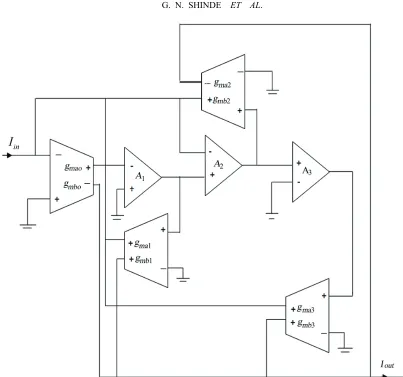
3. Circuit Diagram
The diagram was shown in Figure 1.
4. Circuit Description
Figure 1. Circuit diagram of electronically tunable third order current-mode universal filter.
non-inverting of third OA output of third OA is then fed to v+ terminal fourth OTA. Output terminals of all OTAs carrying positive current are fed to inverting of first OA whereas remaining current output terminals of all OTAs adds to give output current of the circuit. The circuit can realize various third order filter functions by suitably choosing the current output branches.
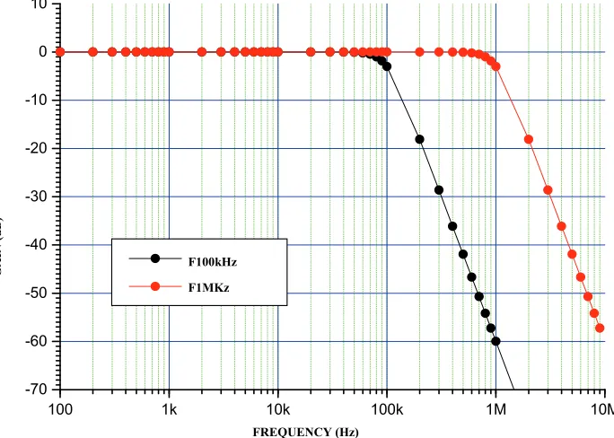
5. Result and Discussion
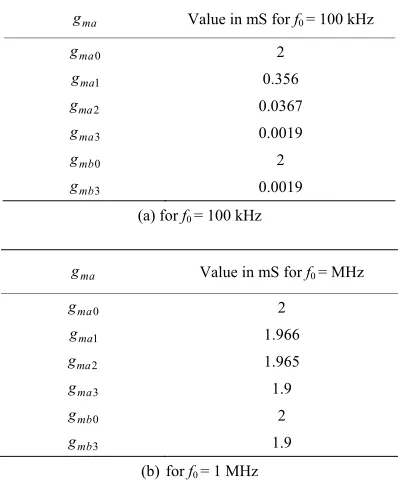
The circuit performance is studied for Central frequen-cies f0 = 100 kHz and 1 MHz with circuit merit factor Q = 1. The general operating range of this filter is 10 Hz to 1 MHz. The value of 123= 6.392 × 10⁶ for LF
356 N. The proposed circuit gives response only for very high frequencies since the values of transconductance of OTAs takes very low values at frequencies less than 100 kHz. The values of gma1,gma2andgma3 are calculated by
taking gma0= 2 and 3 0
1
ma
ma
g
g Response is studied for
Q = 1 for high pass and low pass function. Figures 2 and
3 shows high pass and low pass response of the proposed filter circuit respectively. Data obtained after analysis high pass and low pass response is given in Tables 2 and
3. From Figures 2 and 3, it is seen that the gain roll-off is 18 dB/octave for both the functions and the gain stabi-lizes to 0 dB at frequency 200Hz. There is no overshoot in the response. Observed - 3 dB frequency i.e. cutoff frequency matches with designed value f0. Thus the filter
circuit works ideal for high pass as well as low pass function. The values of transconductance gains for f0=
100 kHz and 1 MHz obtained are given in Tables 1(a)
and (b) respectively.
6. Sensitivities
The practical solution is to design a network that has low sensitivity to element changes [14,15]. Thus sensitivity must be less than limit i.e. unity. The lower the sensitiv-ity of the circuit, the less will its performance deviate because of element changes. The sensitivities 0
68
3 x
S with respect to the circuit active elements are shown in Table 4. These values are within the range
0 y 1
x S
It is found that the proposed circuit has very low sensitivity with respective to active elements.
7. Concluding Remarks
A versatile current-mode active-only filter using OAs and OTAs has been proposed. The proposed circuit can
1k 10k 100k 1M 10M
-70 -60 -50 -40 -30 -20 -10 0 10 20
F100kHz F1MHz
GA
IN(dB)
[image:4.595.126.471.148.391.2]FREQUENCY(Hz)
Figure 2. High pass response of proposed current-mode filter.
100 1k 10k 100k 1M 10M
-70 -60 -50 -40 -30 -20 -10 0 10
F100kHz
F1MKz
GAI
N
(dB)
FREQUENCY(Hz)
Figure 3. Low pass response of proposed current-mode filter.
FREQUENCY (Hz)
GAIN (d
B)
F100kHz F1MHz
FREQUENCY (Hz) F100kHz
F1MKz
GAIN (d
[image:4.595.127.469.447.691.2]Table 1. The values of transconductance gains.
ma
g Value in mS for f0 = 100 kHz
0 ma
g 2
1 ma
g 0.356
2 ma
g 0.0367
3 ma
g 0.0019
0 mb
g 2
3 mb
g 0.0019
(a) for f0= 100 kHz
ma
g Value in mS for f0 = MHz
0 ma
g 2
1 ma
g 1.966
2 ma
g 1.965
3 ma
g 1.9
0 mb
g 2
3 mb
g 1.9
[image:5.595.72.271.102.342.2](b)for f0 = 1 MHz
Table 2. Analysis of frequency response of high pass func- tion for Q = 1.
f0
(kHz)
FOH
(kHz) f( kHz ) 0FOH
Gain Roll-off in
stop band Gain Stabi- lization
dB/Octave starting at Octave ( kHz )
dB FS
(kHz)
100 100 0 18 500 0
1 M 1 M 0 18 500 0 2 M
FOH: –3 dB Frequency FS: Frequency at which gain stabilizes
Table 3. Analysis of frequency response of low pass func-tion for Q = 1.
f0
(kHz)
FOL
(kHz)
f0FOL
( kHz )
Gain Roll-off in stopband
Gain Stabili- zation
dB/Octave
Octave starting
at ( kHz )
dB FS
(Hz )
100 100 0 18 400 0 100
1M 1M 0 18.3 2 M 0 100
FOL: –3 dB Frequency
[image:5.595.57.286.383.488.2]realize the biquadratic transfer function and the circuit characteristics can be electronically tuned by the tran-sconductance gains. From sensitivity analysis, it has been clearly shown that the proposed circuit has very low sen-sitivities with respect to the circuit active elements.
Table 4. Sensitivities 0
x
S and 3
x
S .
The gain roll-off of high pass and low pass configura-tion is 18dB/octave.
8. References
[1] T. Tsutani, T. Higashimura, Y. Sumi and Y. Fukui, “Electonically Tunable Current Mode Active Only Biqu-adratic Filter,” International Journal of Electronics, Vol. 87, No. 3, 2000, pp. 307-314.
[2] C.-C. Hsu and W.-S. Feng, “Dynamic Decoupling and Compensating Methods of Multi-Axis Force Sensors,”
International Journal of Electronics, Vol. 88, No. 1, 2001, pp. 41-51.
[3] I. A. Khan and M. H. Zaidi, “Multifunction Translinear-C Current – Mode Filter,” International Journal of Elec-tonics, Vol. 87, No. 9, 2000, pp. 1047-1051.
[4] M. Higashimura, “Current Mode Low Pass and Band Pass Filters Using the Operational Amplifier Pole,” In-ternational Journal of Electronics, Vol. 74, No. 6, 1993, pp. 945-949.
[5] T. M. Ishida, Y. Fukui and S. Tsuiki, “Novel Electroni-cally Tunable Current Mode Filter without External Pas-sive Elements,” IEEE, Vol. 1, 1996, pp. 262-265. [6] G. W. Roberts and A. S. Sedra, “A General Class of
Cur-rent Amplifier Based Biquadratic Filter Circuits,” IEEE Transactions on Circuits and Systems, Vol. 39, No. 4, 1992, pp. 257-263.
[7] J. Ramirez-Angulo, M. Robinson and E. Sanchez-Sinen- cio, “Current Mode Continuous Time Filters Two Design Approaches,” IEEE Transactions on Circuits and Systems, Vol. 39, No. 6, 1992, pp. 337-341.
[8] N. A. Shah, M. F. Rather, M. A. Malik and S. Z. Iqbal, “Cascadable Electronically Tunable Sito Current Mode Active Only Universal Filter,” ETRI Journal, Vol. 26, 2004, pp. 295-300.
[9] A. K. Mitra and V. K. Aatre, “Low Sensitivity High- Frequency Active R Filters,” I.E.E.E. Transactions on Circuits and Systems, Vol. 23, No. 11, 1976, pp. 670- 676.
[10] G. N. Shinde and P. B. Patil, “Sadhana,” Journal of En-gineering Science,Vol.28, No. 6, 2003, pp. 1919-1926. [11] T. Tsukutani, M. Higashimura, Y. Sumi and Y. Fukui,
“Novel Voltage-Mode Biquad Using Only Active
Devic-x 0
x
S 3
x
S
0 ma
g –1.0–0.33
1 ma
g 0 0
2 ma
g 0 0
3 ma
g 0.33 0
0 mb
g 1.00.33
1
0.33 0
2
0.33 0
3
[image:5.595.59.286.528.644.2]70
es,” International Journal of Electronics, Vol. l87, No. 3, 2000, pp. 307-314.
[12] R. Nandi “Active R Realization of Bilinear RL Imped-ances and their Applications in a High-Q Parallel Reso-nator and External Oscillator,” Proceeding of the Institute of Electrical and Electronics Engineering, Vol. 66, No. 12, 1978, pp. 1666-1668.
[13] G. N. Shinde and D. D. Mulajkar, “Electronically Tuna-ble Current-Mode Second Order High Pass Filter for Different Value of Q,” International Journal of Physical
Sciences,Vol. 3, No. 6, 2008, pp. 148-151.
[14] D. R. Bhaskar, U. R. Sharma and S. M. I. Rizvi, “New Current-Mode Universal Biquadratic Filter,” Microelec-tronic Journal, Vol. 88, No. 10, 1999, pp. 837-839. [15] S. Minaei and S. Turkoz, “Current-Mode Electronically