Device Loss Model of a Fully SiC Based Dual
Active Bridge Considering the Effect of
Synchronous Rectification and Deadtime
Zhenyu Wang
International Academay for Marine Economy and Technology (IAMET)
The University of Nottingham, Ningbo China Ningbo, China
Email: [email protected]
Alberto Castellazzi
Power Electronics Machines and Control Group (PEMC) The University of Nottingham
Nottingham, UK
Email: [email protected]
Abstract—It is becoming a great interest to employ SiC based power devices in dual active bridge (DAB) converter as an alternative to conventional Si-IGBT, due to its higher switching frequency potential, smaller switching losses as well as the capability to operate at synchronous rectification (SR) condition. This paper introduces the device loss model of a SiC MOSFET power module based DAB converter considering the effect of synchronous rectification, and the dead-time effect is also discussed. The calculated device loss for both SiC-MOSFET and Si-IGBT are discussed. The results show that the overall device loss is reduced by 40%, where the conduction loss is reduced by 38%because of SR capability of SiC-MOSFET, and the switching loss is reduced by 48%due to the faster transient of SiC-MOSFET during dead-time. On the other hand, the device losses are not even between the primary bridge and the secondary bridge of the DAB converter, and it is more significant for SiC-MOSFET based DAB due to the effect of SR with a maximum of 20%. At last, the dead-time range is given based on the device properties.
Index Terms—SiC MOSFET power module, Dual Active Bridge Converter, Device Loss, Synchronous Rectification, Dead-time.
I. INTRODUCTION
With the increasing demand of on-board micro-grids, such as aerospace, shipboard or electric vehicle, the power con-verter employed in these applications are required to provide high reliability, high efficiency as well as minimum volume, where dual active bridge (DAB) converters are considered to be one of the options to meet such requirements [1]. The concept of DAB has been proposed for more than two decades [2], Fig 1 shows the basic topology of a DAB converter, which consists of a high-side H-bridge, a high-frequency isolated transformer, a power inductor and a low-side H-bridge. Compared with conventional power transformer, the capability of higher switching frequency of DAB converter, as part of the solid state transformer, reduces the volume of both magnetic components and capacitors. On the other hand, the bi-directional power control ability makes the DAB converter more attractive for on-board micro-grid applications.
Q1 Q2
Q3 Q4
Q5 Q6
Q7 Q8
D1 D2
D3 D4 D7 D8
D6 D5
1:1 L
[image:1.612.313.566.264.339.2]V1 V2
[image:1.612.362.508.364.437.2]Fig. 1. Dual Active Bridge Converter (DAB) Topology
Fig. 2. Employed SiC MOSFET Power Module
The development of silicon carbide (SiC) devices provides DAB converter the capability to reduce the total converter losses as well as the size of the converter compared with Si-IGBT based counterpart. The impact of SiC technology in DAB converter has been discussed [3] [4]. The overall efficiency of commercialized SiC-MOSFET based DAB con-verters are measured and discussed by [5] and [6], the exper-imental results show that a 2-3% efficiency increment can be brought by SiC devices. Moreover, the loss analysis of the SiC-MOSFET based DAB converter are carried out [7]. However, the effect of synchronous rectification of MOSFET as well as the effect of dead-time are not well considered and discussed. This paper will focus on the device properties, including synchronous rectification and device transient performance, to estimate the SiC-MOSFET losses and discuss the impact of device properties in the efficiency of a DAB converter. A fully SiC MOSFET based power module is employed to build the DAB converter, as Fig 2 shows, where the anti-paralleled SiC Schottky diode is included.
and Si-IGBT, and the current model as well as the device conduction loss model considering the effect of synchronous rectification will be given in this section. The modified current model and device conduction loss model including the effect of dead-time will be derived in Section III. Moreover, the transient behavior during dead-time will be analyzed and the switching loss model will be given in this section. Section IV will focus on the dead-time effect, the dead-time range will be given for both SiC-MOSFET based DAB and Si-IGBT based counterpart. The calculated device loss with respect to different dead-time will also be discussed in this section.
II. DUALACTIVEBRIDGECURRENTANALYSIS WITH THE EFFECT OFSYNCHRONOUSRECTIFICATION
Synchronous Rectification (SR) is a generally used tech-nology to reduce the conduction losses based on MOSFET properties. Conventionally, a diode (Schottky diode or body diode of the MOSFET) is used to conduct the reverse current in a converter. However, the P-N junction voltage drop of the diode cannot be neglected. Normally, the voltage drop of Si-based diode is 0.4V and 0.8V for SiC counterpart, which brings a significant power loss to the whole converter. On the other hand, the significant reverse recovery current of Si-based diode not only increases the total loss of the converter, but also slows down the switching speed during turn-off. The idea of SR is to replace the free-wheeling diode by a MOSFET, or try to make the MOSFET operates under SR condition when conducting reverse current to reduce the conduction losses.
Compared with IGBT devices, MOSFET could achieve synchronous rectification because of its unique structure.An additional P layer exists for IGBT compared with MOSFET, which means an additional P-N junction voltage drop exists during the forward conduction of IGBT. On the other hand, the additional P-N junction blocks the reverse current and an anti-paralleled diode is often used to conduct reverse current of the IGBT devices. On the contrary, a MOSFET can be used to conduct reverse current. When the gate (G) of the MOSFET is forward biased, the P layer will temporarily reverse to N type, and creates a current path between drain (D) and source (S), which enables the current flows from both directions. When the gate (G) is reverse biased, a parasitic P-N junction exists in the MOSFET, known as body diode. However, the body diode is not often used due to its bad performance (normally, the voltage drop of the body diode is larger than2V), and an additional anti-paralleled diode is used.
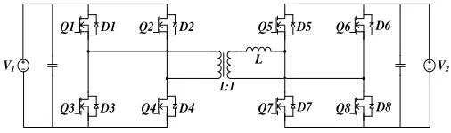
The reverse current path has two conditions when the gate of the MOSFET is forward biased. The reverse current flows only in the channel of the MOSFET under light load (low current), and it will be shared by the MOSFET channel and anti-paralleled diode when the current exceeds a certain level, as shown in Fig.3. The current sharing between the MOSFET channel and anti-paralleled diode can be calculated using (1).
VD−drop+IDRD−on=Vdrop IQRQ−on=Vdrop
ID+IQ=I
(1)
[image:2.612.319.546.50.326.2]Q Dbody D Q Dbody D
Fig. 3. Current Path During Reverse Conduction
−3 −2.5 −2 −1.5 −1 −0.5 0
−400 −350 −300 −250 −200 −150 −100 −50 0
Voltage Drop [V]
Drain−Source Current [A]
Diode only,Vgs=0V MOSFET only,Vgs=20V MOSFET+Diode,Vgs=20V
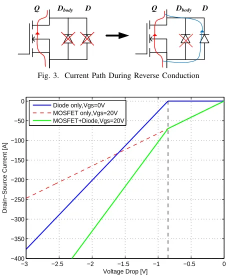
Fig. 4. 3rd Quadrant Characteristics at Room Temperature from Datasheet [8]
Where Vdrop is the total voltage drop across the device, VD−dropis the initial voltage drop of the anti-paralleled diode. I,IQ and ID represent the current flow into the device, the
current shared by MOSFET channel and the current shared by diode, respectively. RQ−on andRD−on represent the
on-resistance for MOSFET channel and anti-paralleled diode. When Vdrop smaller than VD−drop, it is considered that
the current flows only through the channel of the MOSFET, where the body diode as well as the anti-paralleled diode are not conducted due to the insufficient voltage drop, and the MOSFET operates under fully SR. When current increases to a certain level (around 70A in this case, as showed in Fig.4), the voltage drop across the device is high enough to turn-on the anti-paralleled diode, and the current will be shared by the MOSFET channel and the anti-paralleled diode, as showed by the green curve in Fig.4. It is believed that a smaller conduction loss can be brought by the hybrid of SR and anti-paralleled diode conduction compared with the single anti-paralleled diode conduction, as showed in (1) and Fig.4. Moreover, with the increase of the current, the voltage drop increases and it is going to turn on the body diode that the current will be shared by the MOSFET channel, anti-paralleled diode and the body diode. However, the body diode will not be conducted in this case as the current will exceed the current rating of the employed device to get sufficient voltage drop [8].
VPrim
VSec
IPrim, ISec
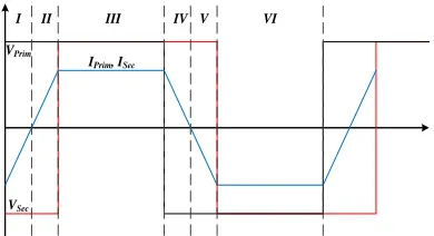
[image:3.612.316.558.49.563.2]I II III IV V VI
Fig. 5. Typical Switching Waveforms of DAB Converter without Dead-time
been made to simplify the analysis.
• The input and output voltage are assumed to be equal and match the transformer ratio.
• The primary bridge is assumed to be the leading bridge and the secondary bridge is the lagging bridge byϕ.
• The initial current of the inductor is assumed to be negative, and the amplitude of the current is large enough to turn on the anti-paralleled diode (larger than 70A in this case) that it is shared by the diode and MOSFET channel.
• The effect of dead-time is temporarily neglected and will
be included in next section.
1) Segment I: During this segment,Q1,Q4on the primary
bridge as well as Q6,Q7 on the secondary bridge are turned on, and the current on the both sides of the transformer in-creases from initial negative peak to zero. It can be concluded that even Q1,Q4 and Q6,Q7 are turned on, the devices on both side of bridge need to conduct reverse current, as shown in Fig.6(a), which means Q1,Q4 and Q6,Q7 are operating under the hybrid of SR and anti-paralleled diode conduction.
2) Segment II: In this segment, the same devices are turned
on as segment I. It should be noted that the current on both sides become positive in this segment, Q1, Q4 and Q6, Q7 start to conduct forward current, as shown in Fig.6(b).
3) Segment III: In this segment, Q1, Q4 on the primary
bridge are turned on whileQ6,Q7on the secondary are turned off. Q5, Q6 are turned on instead. Due to the assumption made earlier, the voltages are assumed to be equal which means there is no voltage difference on the inductor during this segment and the current on both sides of the converter should stay constant. As Fig.6(c) shows,Q1,Q4continue conducting forward current, however, Q5 andQ8 on the secondary will operate under the hybrid mode.
4) Segment IV: WhenQ1,Q4 are turned off,Q2,Q3 are
turned on, a voltage difference appears on the inductor and the current on both sides start to decrease, but stays positive until this segment finishes. It can be noted thatQ2,Q3on the primary side will start to conduct reverse current. The same condition happens to Q5andQ8on the secondary bridge, as Fig.6(d) illustrates.
5) Segment V and VI: Similar with segment II and segment
III,Q2,Q3as well asQ5,Q8conduct forward current during Segment V.Q2,Q3continue conducting forward current while
Q6 and Q7 operate under hybrid mode during Segment VI, as shown in Fig.6(e), (f).
Q1 Q2
Q3 Q4
Q5 Q6
Q7 Q8 D1 D2
D3 D4 D7 D8
D6 D5
1:1 L
V1 V2
(a)
L Q1 Q2
Q3 Q4
Q5 Q6
Q7 Q8 D1 D2
D3 D4 D7 D8
D6 D5
1:1
V1 V2
(b)
L Q1 Q2
Q3 Q4
Q5 Q6
Q7 Q8 D1 D2
D3 D4 D7 D8
D6 D5
1:1
V1 V2
(c)
L Q1 Q2
Q3 Q4
Q5 Q6
Q7 Q8 D1 D2
D3 D4 D7 D8
D6 D5
1:1
V1 V2
(d)
L Q1 Q2
Q3 Q4
Q5 Q6
Q7 Q8 D1 D2
D3 D4 D7 D8
D6 D5
1:1
V1 V2
(e)
L Q1 Q2
Q3 Q4
Q5 Q6
Q7 Q8 D1 D2
D3 D4 D7 D8
D6 D5
1:1
V1 V2
(f)
Fig. 6. DAB Current Analysis with 6 Different Segments
[image:3.612.75.270.53.159.2]C3
C1
C4
C2
IL
IL/2
[image:4.612.318.552.51.515.2]IL/2
Fig. 7. Parasitic Capacitance Current Path during Dead-time (Primary)
IQ3
IC3
ID1
VC3
VC1
td tf tl tDT-td-tf-tl
Fig. 8. Switching Transient during Dead-time (Primary)
III. DEVICELOSSMODEL WITHSRANDDEAD-TIME
An ideal current analysis has been carried out in the previous section and the effect of dead-time is not considered. However, in a real converter, the existence of dead-time affects a lot on the transient behavior of the devices, and it is also believed to affect the overall losses of the SiC MOSFET based converter.
A. DAB Current Model
In order to analyze the effect of dead-time accurately, the transient of the SiC MOSFET current and voltage during dead-time should be discussed. Fig.7 shows the current path of the parasitic capacitance of the devices during switching transient in the dead-time. It is assumed that the inductor current at the beginning the switching transient is negative and stays constant during dead-time,Q2andQ3are turned on before this transient, which means the voltage of the parasitic capacitanceC2,C3are0V, andC1,C4areV1. Once the
turn-off signal is applied to Q2 and Q3, after a certain amount of delay time td, the forward current flow through Q2 and
Q3 will split into two parts. Half of the inductor current is used to discharge C1 from V1 to0V, another half is used to
charge C3 from 0V to V1. The same condition happens for C2 and C4, where C2 is charged while C4 is discharged. It
can be concluded that if the initial inductor current is large enough to charge and discharge the capacitance, the zero voltage switching (ZVS) can be achieved and there will be no turn-on loss.
However, the turn-off loss still needs to be considered. Fig.8 shows the voltage and current waveform during dead-time. As seen in the first part of Fig.8, as discussed before, a certain delay time exists due to the devices properties, and the current
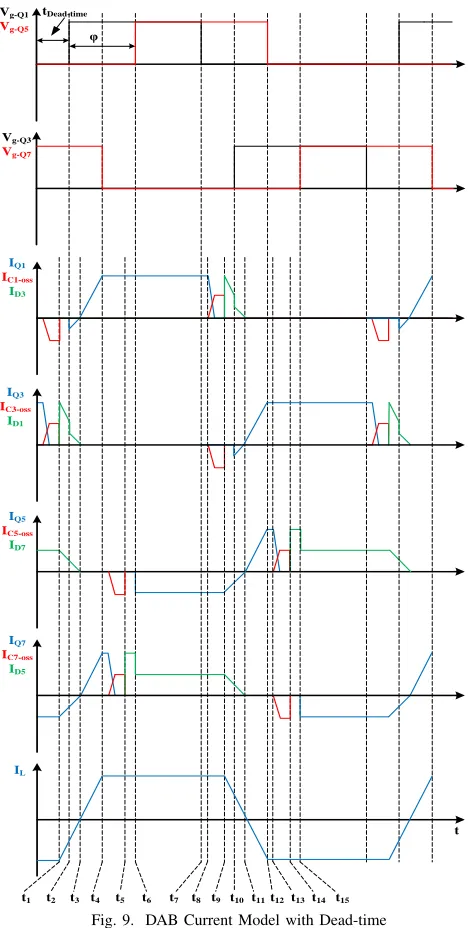
Vg-Q1
Vg-Q5
Vg-Q3
Vg-Q7
IQ1 IC1-oss
ID3
IQ3 IC3-oss
ID1
IQ5 IC5-oss
ID7
IQ7 IC7-oss
ID5
IL
t1 t2 t3 t4 t5 t6 t7 t8 t9 t10 t11t12t13
tDead-time
φ
t14 t15
t
Fig. 9. DAB Current Model with Dead-time
as well as the voltage stay constant during this time. The current of Q3 starts to reduce after td and being split into
the two capacitance, where the capacitance are assumed to be equal in this paper. The voltage ofQ3starts to increase at the same time. The amount of time for this period is tf, which
is also determined by the device properties. The value of the increased voltage during this period can be calculated by (2).
IQ3(t) =−tIL
f t+
IL
tf(td+tf)
VQ3(t) =C1 R
IQ3(t)dt
(2)
AfterQ3current reaches0A, the voltage still needs to increase to the supply voltageV1that the inductor current keep charging
[image:4.612.59.288.51.322.2]be calculated by (3).
tl=
2C IL
(V1−VQ3(td+tf)) (3)
It can be noted from the second part of Fig.8 that the voltage ofQ1has a reverse behavior compare with the voltage ofQ3. The total transient time can be calculated by (4).
ttransient=td+tf+tl (4)
If the total dead-time been set to tDT, as shown in Fig.8,
the remaining time after the transient istDT−ttransient. The
turn-off loss happens duringtf, as can be seen in the blue area
in Fig.8. It should be noted that the voltage is reversed during the transient time that VC1 increases from 0V to V1 while VC3 decreases fromV1 to0V. Thus the current will transfer
from the capacitance into the anti-paralleled diodeD1, where the single anti-paralleled diode conduction loss occurs. On the other hand, the voltage on the primary of the transformer, from the converter point of view, is reversed, therefore the inductor current starts to decrease.
Based on the analysis on the transient behavior during dead-time above, the detailed current waveform including the effect of SR and dead-time for both devices and converter can be derived and presented in Fig.9. The current directions should be clarified. For the SiC MOSFET point of view, the forward current is considered as positive and reverse current is considered as negative in the figure. For the parasitic capacitance, positive current means the capacitor is being charged and negative current means the capacitor is being discharged. Moreover, as seen in the figure, sometimes the current is shared by the anti-paralleled diode and the SiC MOSFET channel (e.g. from t2 tot3 for Q1 andD1 on the
primary bridge, and from t6 to t10 for Q5 and D5 on the
secondary bridge).
Similar with the current analysis in previous section, even the dead-time is included, the six segments still apply. The differences will be the extra single anti-paralleled diode con-duction during dead-time and the small recon-duction caused by the device transient on the phase-shift angle (ϕin Fig.9). The actual phase-shift angle will be ϕ−ttransient2πfsw.
IQ1,D1=
0 (0≤t≤t2)
V1 πfswLωt−
V1(ϕ+2πfswttransient)
2πfswL (t2≤t≤t4)
V1(ϕ−2πfswttransient)
2πfswL (t4≤t≤t8)
0 (t≥t8)
(5)
IQ5,D5=
0 (0≤t≤t6)
−V1(ϕ−2πfswttransient)
2πfswL (t6≤t≤t9)
V1 πfswLωt
−V1(ϕ+2π+2πfsw(ttransient+tDT))
2πfswL (t9≤t≤t12)
V1(ϕ−2πfswttransient)
2πfswL (t12≤t≤t13)
0 (t≥t13)
(6)
ID3−deadtime=
0 (0≤t≤t1)
V1 πfswLωt−
V1(ϕ+2πfswttransient)
2πfswL (t1≤t≤t2)
0 (t≥t2)
(7)
ID7−deadtime=
0 (0≤t≤t14)
V1(ϕ−2πfswttransient)
2πfswL (t14≤t≤t15)
(8)
The current model can be expressed by (5) - (8). It should be noted that the current model for the anti-paralleled diode is only given for the period of dead-time conduction, as the combined equation is given for the current sharing period with the SiC MOSFET channel, and the separated current equation can be derived using (1), (5), (6). It is more meaningful to use the combined equation as the 3rd quadrant characteristics is given based on the current sharing between the channel and anti-paralleled diode, as Fig.4 and [8] showed. Moreover, due to the symmetrical property of the topology, only one device current expression is given for each bridge.
B. Device Loss Model
The device loss model can be derived based on the given current model in previous sub-section, and can be expressed by (9) - (14).
Pcon−Q1,D1=
1
Tsw Z t8
t2
VdropIQ1.D1dt (9)
Pcon−Q5,D5=
1
Tsw Z t12
t6
VdropIQ5.D5dt (10)
TABLE I
CALCULATIONPARAMETERS
Converter Parameters
V1 750V
V2 750V
L 38uH
fsw 20kHz
Device Parameters
Symbol SiC MOSFET Si IGBT td 70ns 250ns tf 22ns 50ns Coss/Coce 5nF 5.5nF
1
Tsw Z t2
t1
VD−dropID3−deadtimedt (11)
Pcon−D5−deadtime=
1
Tsw Z t15
t14
VD−dropID5−deadtimedt (12)
PQ3−of f =
1
Tsw Z td+tf
td
VtItdt (13)
PDevice=
4Pcon−Q1,D1+ 4Pcon−Q5,D5
+ 4Pcon−D3−deadtime+ 4Pcon−D5−deadtime
+ 8PQ3−of f
(14)
Wherefswis the switching frequency of the device.Vdropand VD−drop can be found from the 3rd quadrant characteristics
in Fig.4.
C. Calculated Results
The device losses in a SiC MOSFET power module based DAB converter is calculated using the proposed loss model. For comparison, the device losses of a Si IGBT based DAB converter is also calculated to evaluate the impact of the SiC technology. Noting that the Si IGBT cannot provide the SR capability, and the reverse current will flow through the anti-paralleled diode only. The calculation parameters are illustrated in Table I.
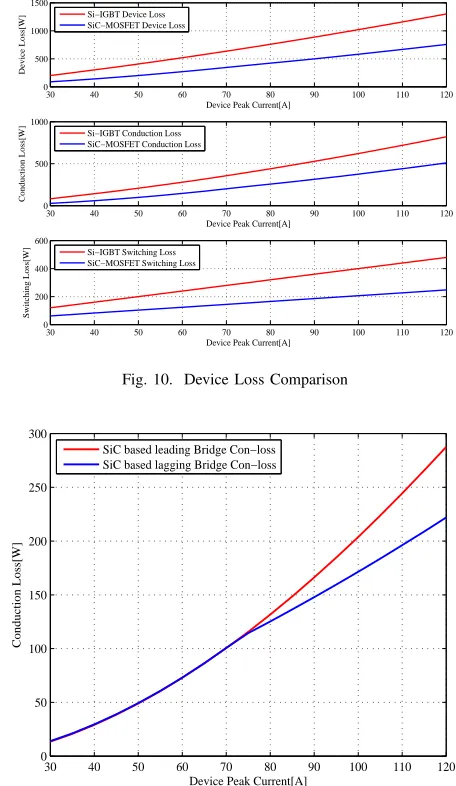
The first part of Fig.10 shows the calculated device losses for SiC MOSFET based DAB and the Si IGBT based coun-terpart. As seen in the figure that a maximum device loss reduction can be achieved by 40% due to the application of SiC MOSFET. Device loss is breakdown into conduction loss and switching loss, which is shown in the second part and thrid part in Fig.10, and it is clear that a significant reduction is observed for both conduction loss and switching loss. The SR capability of SiC MOSFET contributes a lot on reducing the conduction loss with a maximum of 38%. Moreover, the conduction loss difference becomes larger at higher device
30 40 50 60 70 80 90 100 110 120
0 500 1000 1500
Device Peak Current[A]
Device Loss[W]
Si−IGBT Device Loss SiC−MOSFET Device Loss
30 40 50 60 70 80 90 100 110 120
0 500 1000
Device Peak Current[A]
Conduction Loss[W]
Si−IGBT Conduction Loss SiC−MOSFET Conduction Loss
30 40 50 60 70 80 90 100 110 120
0 200 400 600
Device Peak Current[A]
Switching Loss[W]
[image:6.612.45.549.58.452.2]Si−IGBT Switching Loss SiC−MOSFET Switching Loss
Fig. 10. Device Loss Comparison
30 40 50 60 70 80 90 100 110 120
0 50 100 150 200 250 300
Device Peak Current[A]
Conduction Loss[W]
SiC based leading Bridge Con−loss SiC based lagging Bridge Con−loss
Fig. 11. Conduction Losses of the SiC MOSFET based DAB
current, which is the result of the hybrid of SR and anti-paralleled conduction. For the switching loss point of view, a much shorter transient time for SiC MOSFET provides a smaller switching loss. The maximum difference can be observed at 120A by 48%. On the other hand, the reverse recovery effect is not considered for Si IGBT based DAB, and a even larger difference is expected if the reverse recovery effect is included.
[image:6.612.320.548.64.457.2]D. Dead-time Range Discussion
The transient behavior has been analyzed in last sub-section, and the calculation equation to get the total transient time is also discussed in (3), (4), and Fig.8. The calculated transient timettransient is a parameter that related to the load current
and device properties. Moreover, it is also the minimum dead-time to be applied and a smaller dead-dead-time leads to the shoot-through problem of the converter. On the other hand, if the dead-time so large that even larger than half of the phase-shift period, where the inductor current will go across zero point and the directions is reversed, the dead-time effect is expected also known as dead-band effect. The dead-band effect in DAB has been discussed by several papers [9] [10] [11]. Voltage reverse and voltage sag are two major problems that caused by dead-band effect and the maximum dead-time that can be applied will be half of the phase-shift, as shown in (15).
ttransient≤Dead−time≤ ϕ
4πfsw
(15)
IV. CONCLUSION
A detailed device loss model of a SiC MOSFET power module based DAB converter has been proposed in this paper, which considered the effect of synchronous rectification and dead-time. The current of the SiC based DAB is analyzed and it can be concluded that SiC based DAB could provide a much lower conduction loss compared with Si counterpart due to the capability of operating under SR mode. Moreover, the transient behavior is discussed and the switching loss is calculated. Due to a much short transient time, SiC based DAB has lower switching loss. On the other hand, based on the current analysis, the conduction loss breakdown is shown, and it is proved that the lagging bridge has a lower conduction loss compared with primary bridge for SiC based DAB due to the hybrid of SR and anti-paralleled diode conduction. And last, the dead-time range is given. This analytical device loss model provides a method to estimate the device loss accurately using data-sheet values, the experimental validation is undergoing and comparison should be made in the future.
ACKNOWLEDGMENT
This work is partially supported by the Ningbo Science and Technology Bureau, China under Grant 2013A31012.
REFERENCES
[1] B. Zhao, Q. Song, W. Liu, and Y. Sun, “Overview of dual-active-bridge isolated bidirectional dc–dc converter for high-frequency-link power-conversion system,”IEEE Transactions on Power Electronics, vol. 29, no. 8, pp. 4091–4106, 2014.
[2] S. Inoue and H. Akagi, “A bidirectional isolated dc–dc converter as a core circuit of the next-generation medium-voltage power conversion system,”IEEE Transactions on Power Electronics, vol. 22, no. 2, pp. 535–542, 2007.
[3] D. Aggeler, J. Biela, and J. Kolar, “A compact, high voltage 25 kw, 50 khz dc-dc converter based on sic jfets,” in IEEE Applied Power Electronics Conference (APEC), 2008.
[4] A. K. Tripathi, K. Mainali, D. C. Patel, A. Kadavelugu, S. Hazra, S. Bhattacharya, and K. Hatua, “Design considerations of a 15-kv sic igbt-based medium-voltage high-frequency isolated dc–dc converter,”
IEEE Transactions on Industry Applications, vol. 51, no. 4, pp. 3284– 3294, 2015.
[5] Z. Wang, A. Castellazzi, S. Saeed, ´A. Navarro-Rodr´ıguez, and P. Garcia, “Impact of sic technology in a three-port active bridge converter for energy storage integrated solid state transformer applications,” inWide Bandgap Power Devices and Applications (WiPDA), 2016 IEEE 4th Workshop on. IEEE, 2016, pp. 84–89.
[6] D. De, A. Castellazzi, and A. Lamantia, “1.2 kw dual-active bridge converter using sic power mosfets and planar magnetics,” in Power Electronics Conference (IPEC-Hiroshima 2014-ECCE-ASIA), 2014 In-ternational. IEEE, 2014, pp. 2503–2510.
[7] H. Akagi, T. Yamagishi, N. M. L. Tan, S.-i. Kinouchi, Y. Miyazaki, and M. Koyama, “Power-loss breakdown of a 750-v 100-kw 20-khz bidi-rectional isolated dc–dc converter using sic-mosfet/sbd dual modules,”
IEEE Transactions on Industry Applications, vol. 51, no. 1, pp. 420–428, 2015.
[8] CREE, “Datasheet of cas120m12bm2 [online],” Available: www.cree.com.
[9] B. Zhao, Q. Song, W. Liu, and Y. Sun, “Dead-time effect of the high-frequency isolated bidirectional full-bridge dc–dc converter: Com-prehensive theoretical analysis and experimental verification,” IEEE Transactions on Power Electronics, vol. 29, no. 4, pp. 1667–1680, 2014. [10] J. Li, Z. Chen, Z. Shen, P. Mattavelli, J. Liu, and D. Boroyevich, “An adaptive dead-time control scheme for high-switching-frequency dual-active-bridge converter,” inApplied Power Electronics Conference and Exposition (APEC), 2012 Twenty-Seventh Annual IEEE. IEEE, 2012, pp. 1355–1361.