Current Fed Multipulse Rectifier Approach for
Unidirectional HVDC and MVDC Applications
Gustavo Lambert,
Student Member, IEEE,
Marcus V. Soares,
Student Member, IEEE,
Pat Wheeler,
Senior Member, IEEE,
Marcelo L. Heldwein,
Senior Member, IEEE,
and Yales R. de Novaes,
Member, IEEE
Abstract—Even though multipulse rectifiers are a long es-tablished and well-known technology, still their behavior is not fully described in the literature when they are fed by three-phase balanced sinusoidal currents sources. To address the aforementioned gap, this work presents the operation and properties of current-fed multipulse rectifiers. The undertaken aim is achieved by analyzing the examined topology through circuit analysis and then, the theoretical results are validated through comparisons with the simulated waveforms and experi-mental results. Furthermore, the expected harmonic content and the duality with traditional voltage-fed multipulse rectifiers are presented. In the proposed structure, the transformer voltages present a multipulse waveform, instead of its primary currents as in voltage-fed multipulse rectifiers. This implies on limiting the voltage steps and its derivative which might be beneficial to reduce cost and volume of insulation, particularly for MVDC and HVDC applications. Besides that, by actively controlling the primary currents, a possible copper loss reduction is shown in the transformer windings, differentiating the proposed structure from its voltage controlled counterpart.
Index Terms—Multipulse Rectifier, DC-DC, Medium Fre-quency, Current Source.
I. INTRODUCTION
H
IGH-POWER dc-dc converters play an important role enabling the emergent dc grid proposition to have many applications such as electric railways [1], [2], HVDC systems [3], [4], renewable generation [5], [6], all-electric ships [7], dc multi-terminal interconnection [8] and others all of which require a medium or high voltage dc interface. The use of dc offers some advantages over traditional ac links such as the lower conduction losses, the asynchronous operation, the higher active power transfer capability and the absence of low-frequency reactive energy circulation. However, these advantages lead to economically viable solutions typically for long distance scenarios or non-standard applications.Among the cited applications, this paper particularly aims to address the ones with unidirectional power flow through the development of an isolated dc-dc converter for medium or high voltage dc interfaces. In particular, the proposed solution might be advantageously deployed in future subsea transmission and distribution system applied to oil and gas extraction [9], [10] which requires the converter to be: compatible with medium or high voltage, limited in volume and weight, and galvanically isolated.
For the first requirement, compatibility with medium/high voltage, the main options that have been presented in the literature are based on the Dual Active Bridge (DAB) [11],
[12] or based on the Modular Multilevel Converter (MMC) [13], [14]. However, the high dv/dt and the high voltage steps applied in medium/high frequency transformers [15] are still an issue because of their interaction with transformer parasitic elements that may cause two principal effects. The first is current spikes due to capacitive coupling discharges and the second is overvoltages that are caused by leakage inductances [16]. Both interactions are problematic for the converter and may cause malfunction or even its failure.
Subsea engineering applications typically have restrictions with volume and weight, the second requirement. Thus, one known approach is to increase the frequency in the ac stages to reduce the dimensions of the converter. This frequency may be increased from hundreds of hertz up to tens of kilohertz before the losses became problematic. The choice offers an optimization design challenge due to commercially available magnetic material and thermal restrictions [17].
The galvanic isolation between input(s) and output(s) termi-nals is the last requirement. It is important from the operation point of view because it allows the connection of different source or load references (series or parallel). In addition, it enables the fault isolation capability which, for example, is extremely important to avoid the shutdown of large gas and oil production plant [18].
Although a wide variety of isolated converters are pro-posed, which make use of single-phase transformers (mostly expandable to a three-phase configuration), few are proposed using the Multipulse Rectifier (MR) concept [19]. This type of rectifier has long been presented and can be found typically from 12 to 36 pulses in multiples of 6 [20]–[22]. Its main characteristics are the reduction of reactive energy circulation through harmonic cancellation and the higher frequency ripple at the output.
rectifier. It was chosen among the others because of its simplicity and potential to avoid series connection of diodes, specially in the case of MVDC applications. Experimental investigation to support theoretical analysis is also presented.
dc-ac
MF transf. ac-dc
HVDC Line
MVDC Line
[image:2.612.314.561.62.184.2]Analyzed rectifier system
Fig. 1. Two-stage dc-dc converter with medium frequency transformer.
II. FUNDAMENTALS OFMULTIPULSERECTIFIERS
Multipulse Rectifiers are three-phase ac-dc converters de-signed to reduce ac harmonic content when compared to traditional six pulse rectifiers. In general, their elements are summarized by a three-phase phase-shifting element and a set of six pulse rectifiers. For any MR, the required phase difference among each three-phase set (θps) and the number of rectifiers (nr) are related by nr ·θps = π/3. MRs are classified according to particular characteristics, which include its number of pulses and its output rectifiers connection (series, separated or parallel) [20].
The MR harmonic reduction in the primary currents is achieved through harmonic cancellation. The key factor for the harmonic cancellation is the phase difference between each three-phase set in MR’s secondary windings. This angle (θps) cause some secondary current harmonics to be canceled when reflected to the primary windings.
According to the MR number of pulses, a different set of harmonics can be eliminated. The remaining harmonic elements (n) in the input current of a m-pulse rectifier are
n = m k±1, k∈Z+ [23]. For instance, a voltage fed
12-pulse diode rectifier, requires two three-phase systems with the same line voltage and shifted by π/6. If the previous requirements are satisfied, the current through phase “a” is expressed by
ia =I1·sin(ωt) + ∞ X
n=12k±1
In·sin(n ω t), k∈Z+ (1)
where In · sin(n ω t) is the remaining harmonic content. Nonetheless, this cancellation is only complete if the provided phase shift angle is correct and the reflected rectifiers’ currents have the same amplitude. This means that both load differences among rectifiers or turns ratio mismatch among secondaries may cause partial harmonic elimination.
III. CURRENT-FEDMULTIPULSERECTIFIERS: ELEMENTS,
OPERATION ANDCHARACTERISTICS
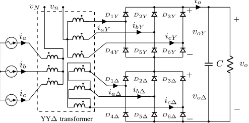
The Current-Fed Multipulse Rectifier (CFMR) differs from Voltage Fed MR (VFMR) due to the presence of a three-phase balanced sinusoidal current source. This means that
ic
ib
ia
D4∆ D1∆
D4Y D1Y
D5∆ D2∆
D5Y D2Y
D6∆ D3∆
D6Y D3Y +
−
voY
+
−
vo∆
io
C
iaY ibY
icY
ia∆ ib∆
ic∆
+
−
vo
vN vn
[image:2.612.66.279.116.202.2]YY∆transformer
Fig. 2. Ideal current-fed 12-pulse series-type diode rectifier topology using a transformer with wye and delta connected secondaries (YY∆-transformer) as the phase-shifting element.
most VFMR arrangements may have its current-fed rectifier version. For the sake of simplicity, this paper focus only in the Current-Fed 12-pulse Rectifier (CFMR) shown in Fig. 2. Furthermore, the series-type was chosen to reduce the need of series connected semiconductors in the bridges, due to voltage restrictions, which may be specially beneficial in medium and high voltage scenarios. The input currents are defined by
ia(t) =Ip·sin(ωt) (2)
ib(t) =Ip·sin(ωt−2π/3) (3)
ic(t) =Ip·sin(ωt+ 2π/3) (4)
and the phase-shift YY∆-transformer’s turns ratios are defined by
n12=
n1
n2
(5)
n13=
n1
n3
(6)
n23=
n2
n3 = √1
3 (7)
wheren1,n2, andn3are the number of turns for the primary, wye-connected secondary, and delta-connected secondary, re-spectively.
A. Current source considerations
Far from ideal sources, the practical CFMR may have two possibilities to implement current sources. The first possibility is to add enough inductance between the voltage source and the primary winding so that the current becomes sinusoidal. The second one is to actively control the MR input currents, i.e., by means of a controlled voltage source.
The second method can be considered an evolution of the first one because it combines the first with a current controlled converter. Therefore, the inductors, if needed, are not as bulky as in the first method since the inductors function is to filter high order harmonic components. This reduces the reactive energy circulation and the ac voltage drop on these inductors. However, it has the following disadvantages: higher number of elements (cost increase), increased complexity (controlled converter), and higher losses (inductor + switching devices).
Nonetheless, the addition of a controlled converter gives more flexibility and functionalities to the structure. Since the obtained advantages are relevant for the target applications, from this point onwards only current sources created by controlled converters are considered.
B. CFMR operation
The CFMR operation is explained considering the 12-pulse rectifier from Fig. 2. It is assumed that the controlled converter and inductors can be summarized by an ideal three-phase balanced current source with frequency ω. Also, the trans-former is assumed to have very low leakage inductances. The simulated currents and voltages waveforms of all windings are shown from Fig. 3 to Fig. 5. These waveforms are vertically scaled using primary peak current (16.67 A) and primary peak voltage (202.78 V) as base values. The output capacitive filter is chosen large enough so that the output voltage vo has a negligible ripple.
As in any MR, each converter’s pulse occurrence in the primary is related to the diode’s switchings at the secondaries. For the 12-pulse rectifier each pulse length is2π/mradians, which equals toπ/6. Also, a unique set of conducting diodes is attributed to each pulse. Since the conducting diodes alternate in a predictable order, for this given particular example, instead of analyzing all the 12-pulses, any set of two adjacent pulses suffices for the analysis.
-1 -0.5 0 0.5 1
Current (pu)
i
a ib ic
-1 -0.5 0 0.5 1
Voltage (pu)
v
aN vbN vcN
0 /3 2 /3 4 /3 5 /3 2
Angle (rad) -1.73
-0.87 0 0.87 1.73
Voltage (pu)
[image:3.612.327.546.52.279.2]vab vbc vca
Fig. 3. Currents and voltages of the wye-connected primary windings.
-2.02 -1.010 1.01 2.02
Current (pu)
iaY ibY icY
-0.23 -0.11 0 0.11 0.23
Voltage (pu)
v
anY vbnY vcnY
0 /3 2 /3 4 /3 5 /3 2
Angle (rad) -0.4
-0.2 0 0.2 0.4
Voltage (pu)
[image:3.612.323.545.317.539.2]vabY vbcY vcaY
Fig. 4. Currents and voltages of the wye-connected secondary windings.
-1.35 -0.670 0.67 1.35
Current (pu)
i
af ibf icf
-2.02 -1.01 0 1.01 2.02
Current (pu)
i
a ib ic
0 /3 2 /3 4 /3 5 /3 2
Angle (rad) -0.4
-0.20 0.2 0.4
Voltage (pu)
vab vbc vca
Fig. 5. Currents and voltages of the delta-connected secondary windings.
Among the available intervals, the interval range from
−π/12 to π/4 is arbitrarily selected. Where the interval 1 ranges from−π/12toπ/12and the interval 2 fromπ/12to
π/4. The input currents waveforms during these intervals are shown in Fig. 6.
The topological state of intervals 1 and 2 are shown in Fig. 7 and Fig. 8, respectively. Note that the currents are defined by the input source, but the voltages across the transformer’s windings are defined by the output voltage as shown in Fig. 3 to Fig. 5.
[image:3.612.65.283.496.724.2]−π/12 0 π/12 π/6 π/4
−1
−0.5 0 0.5 1
Angle (rad)
Current
(pu)
Interval 1 Interval 2
[image:4.612.321.554.97.606.2]ia ib ic
Fig. 6. CFMR input currents (ia,ib,ic) divided in two main intervals.
ic
ib
ia
D4∆
D1∆ D4Y D1Y
D5∆
D2∆ D5Y
D2Y
D6∆
D3∆
D6Y
D3Y +
−
voY
+
−
vo∆
io
Co
+
−
vo
vN vn
YYD transformer
Fig. 7. CFMR static behavior during the interval 1:−π/12≤ωt≤π/12. Nonconducting elements are shown in gray.
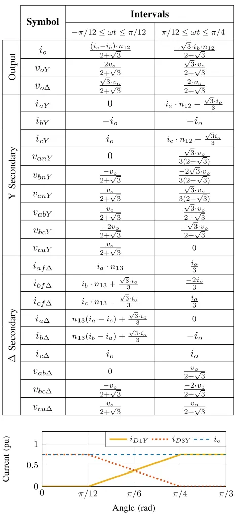
laws and the turns ratio of the shifting transformer on the circuits of Fig. 7 and Fig. 8. The main functions are described in the Table I, wherevabY =vanY−vbnY,vbcY =vbnY−vcnY and vcaY = vcnY −vanY. Together with the turns ratio of the transformer (n12 or n13), some of these voltage functions can be used to derive voltage equations of the wye connected primary winding. Such analysis can be expanded for the whole period regarding the frequencyω.
One distinctive characteristic of CFMR, when compared to VFMR, is that its line current takes one pulse length (π/6
for a 12-pulse rectifier) to be transferred from one diode to another. This is highlighted in Fig. 9, where the current iaY is transferred from D3Y toD1Y. Such behavior can be used to distinguish CFMR from VFMR with low input inductance. It is also noticeable that CFMR phase and line currents at the secondary windings do not have the same sinusoidal waveform as in the primary windings. Moreover, the phase and line voltages of the transformer windings have 12 levels, where the phase voltages are in phase with their respective
ic
ib
ia
D4∆ D1∆ D4Y
D1Y
D5∆
D2∆
D5Y
D2Y
D6∆ D3∆
D6Y
D3Y +
−
voY
+
−
vo∆
io
Co
+
−
vo
vN vn
YYD transformer
Fig. 8. CFMR static behavior during the interval 2: π/12≤ ωt≤ π/4. Nonconducting elements are shown in gray.
TABLE I
CURRENTS AND VOLTAGES OF THECFMRWRITTEN AS FUNCTIONS OF THE INPUT CURRENTS AND OUTPUT VOLTAGE FOR THE TWO CONSIDERED
INTERVALS OFωt
Symbol Intervals
−π/12≤ωt≤π/12 π/12≤ωt≤π/4
Output
io
(ic−ib)·n12
2+√3
−√3·ib·n12
2+√3
voY 2+2v√o3
√ 3·vo 2+√3
vo∆
√ 3·vo 2+√3
2·vo 2+√3
Y
Secondary
iaY 0 ia·n12−
√
3·io
3
ibY −io −io
icY io ic·n12−
√
3io
3
vanY 0
√ 3·vo 3(2+√3)
vbnY 2+−v√o3 −2
√ 3·vo 3(2+√3)
vcnY 2+v√o3
√ 3·vo 3(2+√3)
vabY 2+v√o3
√ 3·vo 2+√3
vbcY 2+−2√vo3 −
√ 3·vo 2+√3
vcaY 2+v√o3 0
∆
Secondary
iaf∆ ia·n13 i3o
ibf∆ ib·n13+
√
3·io
3
−2io 3
icf∆ ic·n13−
√
3·io
3
io 3
ia∆ n13(ia−ic) +
√
3·io
3 0
ib∆ n13(ib−ia) +
√
3·io
3 −io
ic∆ io io
vab∆ 0 2+v√o3
vbc∆ 2+−v√o3 −2+2·√vo3
vca∆ 2+v√o3 2+v√o3
0 π/12 π/6 π/4 π/3
0 0.5 1
Angle (rad)
Current
(pu)
[image:4.612.49.298.194.303.2]iD1Y iD3Y io
Fig. 9. Current transfer from the diodeD3Y to the diodeD1Y during one
pulse of the 12-pulse rectifier output current. The base values are the primary current peak value(iapk= 16.67) and the primary phase voltage peak value
(vb= 202.7)
phase currents.
[image:4.612.49.300.609.717.2]at the output to obtain a desired voltage ripple target.
0 π/3 2π/3 π 4π/3 5π/3 2π
0.6 0.7 0.8
Angle (rad)
Current
[image:5.612.54.292.80.159.2](pu)
Fig. 10. CFMR output currentio waveform.
Although the output can be seen as a voltage source, the output voltage is a consequence of the controlled current at the primary. Thus, the mean value of the output current (Io) is an important figure, and can be obtained from one of the previously analyzed intervals, since this current repeat its behavior at every π/6 regarding ω. The mean value of the output current (Io) as a function of input peak current and transformer turns ratio is presented in (9).
Io=
12·2 2π
Z 12π
0
(ic−ib)·n12
2 +√3 dθ (8)
Io=
3√6·(√3−1)·n12·Ip
π(2 +√3) (9)
C. Harmonics cancellation and distribution
[image:5.612.323.552.83.255.2]The CFMR main variables harmonic content is shown in Fig. 11. The harmonic composition has two main charac-teristics to be noted. First, the phase voltage (vaN) has the harmonics that would appear in a VFMR primary current. Sec-ond, although primary currents are sinusoidal, some harmonics appear on the secondary currents. These harmonics are verified by the theoretical composition presented in Table II.
These harmonics on the secondary-side currents, although not obvious, are mathematically explained since they are canceled by the phase-shift element on the primary windings. So, in the 12-pulse case, the harmonics that appear on the secondary currents are defined by6·(2k−1)±1wherek∈Z+. As a consequence of the harmonic content, the CFMR has a potential reduction in the copper losses in comparison with the VFMR. Because only pure sinusoidal currents flow into the transformer’s primary windings, and then= 12k±1, k∈Z+,
harmonics are suppressed on the secondary windings. However, the n = 12k±1, k ∈ Z+ order harmonics
that appear in the transformer voltages generate an increased
3 5 7 9 11 13 15 17 19 21 23 25 27 29 31 0%
3%
6%
9%
12%
15%
Harmonics
Harm./Fund.
vaN iaY ia∆f
Fig. 11. Single-sided FFT spectrum of primary phase voltage (vaNin yellow)
and secondary windings currents (iaY in blue andia∆f in red).
TABLE II
DUALITY BETWEENCFMRANDVFMRCURRENTS AND VOLTAGES
Symbol Harmonic composition
VFMR
iaY
∞
P
n=1,5,7,11,13,17,19,...
In·sin(n ω t)
ia∆
∞
P
n=1,5,7,11,13,17,19,...
In·sin(n ω t−30◦)
ia I1·sin(ωt) +
∞
P
n=12k±1
In·sin(n ω t)
vaN V1·sin(ωt)
CFMR
iaY
∞
P
n=1,5,7,17,19,...
In·sin(n ω t)
ia∆
∞
P
n=1,5,7,17,19,...
In·sin(n ω t−30◦)
ia I1·sin(ωt)
vaN V1·sin(ωt) +
∞
P
n=12k±1
Vn·sin(n ω t)
amount of alternated magnetic flux in the transformer magne-tizing inductance. This can cause some elevation in the CFMR transformer core losses when compared to VFMR, due to the multilevel waveform voltage, but reduces the transformer’s voltage steps.
Finally, the high-frequency switching harmonics, from the controlled voltage source, usually do not appear on the MR transformer’s core. Because inductors are added to ease the current control, the critical core losses due to the large voltage high-frequency variations appear mostly on them, which are less expensive magnetic elements than the MF transformer.
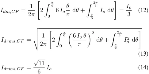
D. VFMR and CFMR diode current evaluation
To evaluate the average (Idm) and rms (Idrms) values of a diode’s current, it is assumed a VFMR series-type with very high output filter capacitance and low primary side inductances as presented in [20]. For such VFMR, each secondary side line currents has a trapezoidal waveform with four humps for the positive cycle and another four for the negative cycle. Each hump has a length ofπ/6radians and the converter is assumed to operate in continuous conducting mode. These humps are assumed to provide a negligible current variation. Thus, the current can be approximated by the mean value of the rectifier output current (Io). For a conducting interval of2π/3radians, the mean and the rms values of each diode current are
Idm,V F =
1 2π
Z 2π/3
0
Iodθ=
Io
3 (10)
Idrms,V F = s
1 2π
Z 2π/3
0
I2 o dθ=
√ 3
3 Io. (11)
[image:5.612.105.249.302.358.2] [image:5.612.352.561.606.671.2]Idm,CF =
1 2π
"
2
Z π6
0 6Io
θ π dθ+
Z 23π
π
6
Io dθ #
= Io 3 (12)
Idrms,CF = v u u t
1 2π
"
2
Z π6
0
6I
oθ
π
2
dθ+
Z 23π
π
6 I2
o dθ #
(13)
Idrms,CF =
√ 11
6 Io (14)
Equations (10) and (12) show no difference between diodes average currents for both structures (VFMR and CFMR). However, Idrms,V F andIdrms,CF ratio
Idrms,V F
Idrms,CF
= Io √
3 3 ·
6
Io
√
11 ≈1.0445 (15)
reveals that for the specified configuration the diodes current rms value is 4.45 % higher than in the CFMR case, which implies in a slight decrease on each diode conduction loss.
E. CFMR power considerations
Due to the multipulse technique, the CFMR has inherently a high power factor (active power and apparent power ratio). However, besides the harmonic content, a significant amount of reactive energy may appear due to the required inductors. Assuming just the fundamental frequency, the reactive energy is estimated by the angle (θre) between the source’s (~vin) and the transformer’s (~b1) phase voltage phasor. These pha-sors are shown in Fig. 12 considering the inductor’s phasor
~
vL = Ip · ω · L∠90◦.
~vL
~b1
~ vin
[image:6.612.58.301.69.190.2]θre
Fig. 12. Voltage phasors diagram
To calculate the angle, it is still necessary to obtain the fundamental of the multilevel primary phase voltage. The amplitude of this phasor is obtained decomposing its waveform into its Fourier series. Then, it is expressed as a function of the CFMR output voltage (vo), as
|b1|=
6√2·(√3 + 1)
12 + 7√3 ·
vo·n12
π . (16)
Applying Kirchhoff’s voltage law in a primary phase and considering no common mode voltage, the input voltage source has to provide a fundamental component with an am-plitude (|vin|) and a phase (θre) that matches with the phasors diagram shown in Fig. 12. Therefore, the phase between the input voltage fundamental component and the input current, which is ideally sinusoidal, can be expressed by
θre= arctan
I
p·ω·L
b1
. (17)
Analyzing these phasors with a constant output voltage value (constant value ofb1), it can be seen thatθreis increased either by using a higher inductance value or by increasing the peak value of the CFMR input current (Ip). Also, a trade-off between easing the input current control by increasing the input inductance and the amount of reactive energy that the controlled voltage source has to process is noticed.
F. Transformer voltage steps
The voltage across the windings of the CFMR transformer has limited voltage steps as depicted in Fig. 3. This multi-pulse waveform is shaped accordingly to the output rectifiers switching state where the step amplitude is fixed, but varies from one level to another. For instance,vaN voltage step from 0 pu to the following level is visually much higher than the step from 1 pu to the following level.
Since the biggest voltage step implies the highest voltage stress across the winding, it is relevant to determine its value. Such step is identified to happen (from the presented waveforms) during the phase voltage transition going to 0 pu or from 0 pu (see Fig. 3). The maximum phase voltage step (∆vph,max) can be calculated from the difference between each voltage interval provided in Table I. Regarding the primary phase voltage, it is
∆vph,max=
n12·Vo
2·√3 + 3 . (18)
In order to compare the voltage steps applied over the transformer windings with other isolated topologies, the value
∆vph,max/(n·Vo)is created as a figure of merit. In addition, it is assumed that the converters operate in a step-down mode, the ratio between primary and secondary windings to ben, and the primary windings series inductance to be much higher than the secondary winding inductance.
For converters based on parallel or series connected single-phase Single Active Bridge modules [24], the maximum voltage step on each transformer is ∆vph,max/(n·Vo) = 2. However, if the modules are updated into a three-phase con-figuration with 6-pulse rectifier [25], the figure of merit can be reduced to1/3. In the case of MMC based converters, as the two MMC connected through a transformer in [14], the voltage stress on the windings is related to the applied modulation and usually has a∆vph,max/(n·Vo)as function of1/N whereN is the number of submodules per arm [26].
+
−
Vi
ia
a
ib
b
ic
c
a Lp
b
Lp
c Lp
D4∆ D1∆
D4Y D1Y
D5∆ D2∆
D5Y D2Y
D6∆ D3∆
D6Y D3Y +
−
VoY
+
−
Vo∆
io
Co
iaY ibY
icY
ia∆ ib∆
ic∆
+
−
Vo
VN Vn
[image:7.612.58.290.241.386.2]YY∆transformer
Fig. 13. Experimental circuit diagram composed of MMC with two half-bridge submodules per arm and series-type 12-pulse rectifier.
MMC
MR Control boards
Fig. 14. Dc-dc CFMR prototype composed by MMC (middle), 12-pulse rectifier (left) and the system control boards (right).
the dc-ac stage to operate with higher output voltage steps and higher switching frequency than the traditional two-stage dc-dc converters.
IV. DISCUSSION ANDEXPERIMENTAL RESULTS
The experimental verification was performed by using the dc-dc converter that is shown in Fig. 14. Such converter is composed of a Modular Multilevel Converter (MMC) operat-ing as a controlled three-phase current source and a series-type 12-pulse rectifier. Both are detailed in the diagram presented in Fig. 13. Details about the control strategy can be found in [27]. This structure has the inherent features of the MMC plus the isolation of the CFMR also, due to the stacked six-pulse bridges, MVDC levels are easily achieved without the need of series connected diodes. All the experimental waveforms were acquired using a Mixed Signal Oscilloscope Tektronix MSO2014B.
The voltage levels in the experiment were defined based on the interface between a dc transmission line (160 kV) and a dc distribution line (15 kV) which was part of previous research on energy delivery to subsea loads [10]. To maintain a similar voltage reduction, the output voltage was rounded to 60 V since the available input dc source in the laboratory was limited to 650 V.
The CFMR passive elements (Co andLp) were chosen to keep each input phase current ripple and the output voltage
Time (2 ms/div) -10
-5 0 5 10 15 20
Current [A]
20 30 40 50 60 70 80
[image:7.612.317.557.242.352.2]Voltage [V]
Fig. 15. Output voltage (vo) and input currents (ia,ib andic) waveforms.
The output voltage mean value is60.4 Vand the rms values ofia,ib, andic
are4.11 A,3.86 A, and4.13 A, respectively. The sample interval is 1.92 µs.
ripple low. The ac link frequency (f) was chosen to reduce the magnetic elements volume but without increasing significantly the core losses since both transformer and MMC’s inductors cores are made of silicon steel. These parameters are summa-rized in Table III.
TABLE III
DC-DCCONVERTER PARAMETERS
Parameter Value Parameter Value
N 2 Ro 3.75 Ω
Co 270µF Vi 650 V
Lp 2.8 mH Vo 60 V
f 400 Hz n12 6.5
[image:7.612.338.536.503.567.2]Time (2 ms/div)
-20 -10 0 10 20
Current [A]
Fig. 16. Secondary side wye-connected windings currents (iaY, ibY andicY) and primary side current (ia). The rms values of
these currents are, respectively: 12.8 A,12.6 A, 13.2 A, and 4.28 A. The sample interval is 1.92 µs.
-20 -10 0 10 20
Current [A]
Fig. 17. Secondary side delta-connected line currents (ia∆, ib∆and ic∆)
and primary side current (ia) waveforms. The rms values of these currents
are, respectively:12.8 A,12.6 A,13.3 A, and4.28 A. The sample interval is 1.92 µs.
the acquired waveforms.
The primary side transformer phase voltages are presented in Fig. 18. In this figure, one can verify the 12-pulse waveform pattern also seen in the simulated waveforms in Fig. 3. Considering the presented voltage and current RMS values a total of 382.23 VA is calculated. Assuming the same value for the other phases, the input apparent power calculated is
1146.69 VA which results in a near 0.85 power factor. From the derivation in Section III-E, we know that at least an angle of 21.6◦ is expected, which only by itself would contribute to a power factor close to 0.92. Considering the remaining harmonics, the obtained power factor is plausible. To reduce it, the first attempt should concern reducing the input inductance. Although phase voltage and phase current should be in phase, a small angle between the transformer’s phase voltage (vaN) and current (ia) is noticed in Fig. 18. This angle is expected to appear in the experimental results due to the leakage inductance.
The biggest phase-voltage step in Fig. 18 is measured to be compared with the theoretical one from (18) which gives approximately 60.4 V. Due to the high-frequency noise, the calculation of the step for each phase is made through the difference between the average voltage of each pulse. This results in ∆vaN,max = 61.1 V, ∆vbN,max = 58.8 V and
∆vcN,max= 66.8V.
One particular verification is noticed on both secundary windings line voltages as shown in Fig.19. It was found that these line voltages differ from the simulated ones shown in section III-B due to the secondary leakage inductance. Since
Time (1 ms/div) -300
-200 -100 0 100 200 300
Voltage [V]
-30 -20 -10 0 10 20 30
[image:8.612.52.297.56.169.2]Current [A]
Fig. 18. Primary side phase voltages (vaN, vbN,andvcN) and primary side
current (ia) waveforms. The rms values of the voltages are94.7 V,94.0 V
and102 V. The sample interval is0.08µs.
Time (1 ms/div) -60
-40 -20 0 20 40 60
Voltage [V]
-15 -10 -5 0 5 10 15
Current [A]
Fig. 19. Secondary side delta-connected voltages waveforms (vab∆, vbc∆,andvca∆) and primary side phase current waveform
(ia). The sample interval is0.08µs.
the prototype has a different leakage inductance than the simulated one, the bigger voltage drop is enough to turn on a diode in parallel to the conducting one. This causes a longer zero voltage interval to appear (π/6 radians longer). Further than the leakage itself, this phenomenon is also dependent on the converter’s di/dt and on the output voltage level because the resulting voltage must overcome the instantaneous diode blocking voltage. However, even if the secondary line voltage harmonic content is changed, no further differences are observed in the operation.
Finally, one diode of each six-pulse rectifier is monitored and their voltages are shown in Fig. 20. During the blocking interval, each rectifier’s output voltage step can be verified. It is important to notice that the output voltage of each six-pulse bridge alternate between two different voltage levels defined in Table I: 2vo/(2 +
√
3) = 32.1 V, and √3vo/(2 +
√ 3) = 27.8 V. These voltage levels also appear in the secondary line voltages shown in Fig. 19.
V. CONCLUSION
An analysis of current-fed multipulse rectifiers was pre-sented with the particular characterization of 12-pulse diode rectifiers. Such analysis allowed new observations of a clas-sic ac-dc topology, in special its duality with the VFMR. The CFMR operation and harmonic characteristics have been proven by theoretical analysis and experimental results.
[image:8.612.316.558.57.170.2] [image:8.612.317.555.217.333.2] [image:8.612.53.296.226.338.2]frequency--20 -15 -10 -5 0 5 10 15 20
Current [A]
-20 -10 0 10 20 30 40 50 60
[image:9.612.52.295.59.167.2]Voltage [V]
Fig. 20. Diodes voltages waveforms considering blocking voltage as positive value for D1Y (vdp) and for D1∆ (vdn). Also, primary phase current
waveform (ia) and secondary star connected line current waveform (iaY).
The rms value of each voltage is26.1 V,23.7 V, and26.5 V. The rms value of the current is4.33 A. The sample interval is0.08µs.
link. Not only the link frequency but also the multipulse effects enable to reduce filters size and weight for the whole converter. The CFMR also benefits the applications due to the limited voltage steps on the power transformer and inherent current limitation capability. The last characteristic, is a very important safety feature that may ease the fault handling and system operation. In addition, further than safety reasons, the output isolation also offers to the target applications the flexibility to connect different loads references.
ACKNOWLEDGMENT
The authors would like to thank PETROBRAS for the resources and technical discussions under the project process number 2012/00003-7. Also, thanks FAPESC, CAPES and FITEJ for the funding and the support to our research lab-oratory (nPEE).
REFERENCES
[1] N. H. Baars, J. Everts, H. Huisman, J. L. Duarte, and E. A. Lomonova, “A 80-kw isolated dc-dc converter for railway applications,”IEEE Trans. Power Electron., vol. 30, no. 12, pp. 6639–6647, Dec 2015.
[2] A. G´omez-Exp´osito, J. M. Mauricio, and J. M. Maza-Ortega, “Vsc-based mvdc railway electrification system,”IEEE Trans. Power Del., vol. 29, no. 1, pp. 422–431, Feb 2014.
[3] T. L¨uth, M. M. C. Merlin, T. C. Green, F. Hassan, and C. D. Barker, “High-frequency operation of a dc/ac/dc system for hvdc applications,”
IEEE Trans. Power Electron., vol. 29, no. 8, pp. 4107–4115, Aug 2014. [4] B. Zhao, Q. Song, J. Li, Q. Sun, and W. Liu, “Full-process operation, control, and experiments of modular high-frequency-link dc transformer based on dual active bridge for flexible mvdc distribution: A practical tutorial,”IEEE Trans. Power Electron., vol. 32, no. 9, pp. 6751–6766, Sept 2017.
[5] Y. Liu, H. Abu-Rub, and B. Ge, “Front-end isolated quasi-z-source dc-dc converter modules in series for high-power photovoltaic systems-part i: Configuration, operation, and evaluation,”IEEE Trans. Ind. Electron., vol. 64, no. 1, pp. 347–358, Jan 2017.
[6] S. P. Engel, M. Stieneker, N. Soltau, S. Rabiee, H. Stagge, and R. W. D. Doncker, “Comparison of the modular multilevel dc converter and the dual-active bridge converter for power conversion in hvdc and mvdc grids,”IEEE Trans. Power Electron., vol. 30, no. 1, pp. 124–137, Jan 2015.
[7] N. Doerry and K. Moniri, “Specifications and standards for the electric warship,” in2013 IEEE Electric Ship Technologies Symposium (ESTS), April 2013, pp. 21–28.
[8] Z. Suo, G. Li, L. Xu, R. Li, W. Wang, and Y. Chi, “Hybrid modular multilevel converter based multi-terminal dc/dc converter with min-imised full-bridge submodules ratio considering dc fault isolation,”IET Renewable Power Generation, vol. 10, no. 10, pp. 1587–1596, 2016.
[9] A. Mohammadpour, L. Parsa, M. H. Todorovic, R. Lai, and R. Datta, “Interleaved multi-phase zcs isolated dc-dc converter for sub-sea power distribution,” in IECON 2013 - 39th Annual Conference of the IEEE Industrial Electronics Society, Nov 2013, pp. 924–929.
[10] G. Lambert, Y. R. Novaes, and M. L. Heldwein, “Dc-dc high power converter,” inPCIM South America 2014, International Conference and Exhibition for Power Electronics, Intelligent Motion, Renewable Energy and Energy Management 1st Edition, 2014.
[11] L. Wang, Q. Zhu, W. Yu, and A. Q. Huang, “A voltage medium-frequency isolated dc-dc converter based on 15-kv sic mosfets,”IEEE Journal of Emerging and Selected Topics in Power Electronics, vol. 5, no. 1, pp. 100–109, March 2017.
[12] Y. Lee, A. J. Watson, G. Vakil, and P. W. Wheeler, “Design con-siderations for a high-power dual active bridge dc-dc converter with galvanically isolated transformer,” in 2017 IEEE Energy Conversion Congress and Exposition (ECCE), Oct 2017, pp. 4531–4537. [13] B. Zhao, Q. Song, J. Li, Y. Wang, and W. Liu, “Modular multilevel
high-frequency-link dc transformer based on dual active phase-shift principle for medium-voltage dc power distribution application,” IEEE Trans. Power Electron., vol. 32, no. 3, pp. 1779–1791, March 2017. [14] S. Kenzelmann, A. Rufer, D. Dujic, F. Canales, and Y. De Novaes,
“Isolated dc/dc structure based on modular multilevel converter,”IEEE Trans. Power Electron., vol. 30, no. 1, pp. 89–98, Jan 2015.
[15] T. Guillod, F. Krismer, and J. W. Kolar, “Electrical shielding of mv/mf transformers subjected to high dv/dt pwm voltages,” in 2017 IEEE Applied Power Electronics Conference and Exposition (APEC), March 2017, pp. 2502–2510.
[16] A. K. Tripathi, K. Mainali, S. Madhusoodhanan, A. Kadavelugu, K. Vechalapu, D. C. Patel, S. Hazra, S. Bhattacharya, and K. Hatua, “A novel zvs range enhancement technique of a high-voltage dual active bridge converter using series injection,”IEEE Trans. Power Electron., vol. 32, no. 6, pp. 4231–4245, June 2017.
[17] M. A. Bahmani, “Design considerations of medium-frequency power transformers in hvdc applications,” in2017 Twelfth International Con-ference on Ecological Vehicles and Renewable Energies (EVER), April 2017, pp. 1–6.
[18] J. Song-Manguelle, M. H. Todorovic, R. K. Gupta, D. Zhang, S. Chi, L. J. Garc´es, R. Datta, and R. Lai, “A modular stacked dc transmission and distribution system for long distance subsea applications,” IEEE Transactions on Industry Applications, vol. 50, no. 5, pp. 3512–3524, Sept 2014.
[19] A. K. Tripathi, K. Mainali, D. C. Patel, A. Kadavelugu, S. Hazra, S. Bhattacharya, and K. Hatua, “Design considerations of a 15-kv sic igbt-based medium-voltage high-frequency isolated dc-dc converter,”
IEEE Trans. Ind. Appl., vol. 51, no. 4, pp. 3284–3294, July 2015. [20] B. Wu,High-Power Converters and AC Drives. Wiley, 2006, ch. 5,
pp. 83–92.
[21] B. Singh, S. Gairola, B. N. Singh, A. Chandra, and K. Al-Haddad, “Multipulse ac-dc converters for improving power quality: A review,”
IEEE Trans. Power Electron., vol. 23, no. 1, pp. 260–281, Jan 2008. [22] B. Singh, B. N. Singh, A. Chandra, K. Al-Haddad, A. Pandey, and
D. P. Kothari, “A review of three-phase improved power quality ac-dc converters,”IEEE Trans. Ind. Electron., vol. 51, no. 3, pp. 641–660, June 2004.
[23] D. A. Paice,Power Electronics Converter Harmonics: Multipulse Meth-ods for Clean Power. Wiley-IEEE Press, 1996, ch. 3, pp. 25–37. [24] Y. Ting, S. de Haan, and B. Ferreira, “Modular single-active bridge
dc-dc converters: Efficiency optimization over a wide load range,” IEEE Industry Applications Magazine, vol. 22, no. 5, pp. 43–52, Sept 2016. [25] E. A. Jr. and I. Barbi, “Three-phase three-level pwm dc-dc converter,”
IEEE Transactions on Power Electronics, vol. 26, no. 7, pp. 1847–1856, July 2011.
[26] I. A. Gowaid, G. P. Adam, S. Ahmed, D. Holliday, and B. W. Williams, “Analysis and design of a modular multilevel converter with trapezoidal modulation for medium and high voltage dc-dc transformers,” IEEE Transactions on Power Electronics, vol. 30, no. 10, pp. 5439–5457, Oct 2015.
Gustavo Lambert (S”14) received the B.S. and M.S. degrees in electrical engineering from the Santa Catarina State University (UDESC), Joinville, Brazil, in 2012 and 2015, respectively. He is cur-rently pursuing the Dr. degree at Santa Catarina State University. His research interests include the design and control of modular multilevel converter topologies for HVDC and MVDC applications.
Marcus V. Soares received the B. E. degree in
electrical engineering from the Santa Catarina State University, Joinville, SC, Brazil, in 2015. He is currently working toward the Ph.D degree at the Santa Catarina State University. His research in-terests include dc-dc converter structures for HVdc transmission and MVdc distribution networks.
Patrick Wheeler(M’00–SM’12) received his BEng
[Hons] degree in 1990 from the University of Bristol, UK. He received his PhD degree in Electrical Engi-neering for his work on Matrix Converters from the University of Bristol, UK in 1994. In 1993 he moved to the University of Nottingham and worked as a research assistant in the Department of Electrical and Electronic Engineering. In 1996 he became a Lecturer in the Power Electronics, Machines and Control Group at the University of Nottingham, UK. Since January 2008 he has been a Full Professor in the same research group. He is currently Head of the Department of Electrical and Electronic Engineering at the University of Nottingham. He is an IEEE PELs ‘Member at Large’ and an IEEE PELs Distinguished Lecturer. He has published 400 academic publications in leading international conferences and journals.
Marcelo Lobo Heldwein (S”99-M”08-SM’13)
re-ceived the B.S. and M.S. degrees in electrical engineering from the Federal University of Santa Catarina (UFSC), Florian´opolis, Brazil, in 1997 and 1999, respectively, and his Ph.D. degree from the Swiss Federal Institute of Technology (ETH Zurich), Zurich, Switzerland, in 2007.
He is currently an Associate Professor with the Department of Electronics and Electrical Engineer-ing at the UFSC.
From 1999 to 2003, he worked with industry, including R&D activities at the Power Electronics Institute, Brazil and Emerson Network Power, Brazil and Sweden. He was a Postdoctoral Fellow at the ETH Zurich and at the UFSC from 2007 to 2009. Dr. Heldwein is a member of the Brazilian Power Electronic Society (SOBRAEP).
His research interests include Power Electronics, Advanced Power Distri-bution Technologies and Electromagnetic Compatibility.
Yales Romulo de NovaesYales Rˆomulo De Novaes