ANALYSIS AND DESIGN OF A PUSH
Department of EEE, Vijay Rural En
ARTICLE INFO ABSTRACT
This project presents a power transition
integrating two boost inductors into one magnetic core, not only the circuit volume is reduced, but also the op
power-conduction losses of the switches and both the turns and diameters of th advantages of a TM boost PFC, such as quasi
current switching (ZCS) of the output diode, are maintained to improve the overall conversion efficiency. The hardware design is impl
Copyright © 2015 Dr. Balakrishna Reddy. This is an open access article distributed under the Creative Commons Att use, distribution, and reproduction in any medium, provided the original work is properly cited.
INTRODUCTION
To increase the power rating of a TM boost PFC to the medium level without raising the EMI issue and increasing the current stresses of the circuit elements, an interleaved TM boost PFC is recently proposed. Derived from two TM boost converters with the interleaved operations, the power rating is increased and the input current and output current are shared equally with lower current ripples. Therefore, the total harmonic distortion (THD) of input current and the output capacitance can be reduced. However, the need of two inductors with two independent cores increases the circuit volume. In this paper, a push–pull boost PFC composed of two interleaved TM boost PFCs and a coupled inductor is proposed. A single magnetic core is used. The two identical modules can share the output power and promote the power capability up to the medium-power-level applications. In addition, coupling the two distributed boost inductors into a single magnetic core substantially reduces the circuit volume and the cost, which are the important targets of the development of switching power supply today. The interleaved operations of the switches act like a push–pull
*Corresponding author: Dr. Balakrishna Reddy, V.
Department of EEE, Vijay Rural Engineering College, Nizamabad, Telangana State, India.
ISSN: 0975-833X
Article History:
Received 26th March, 2015 Received in revised form 12th April, 2015 Accepted 29th May, 2015 Published online 30th June,2015
Key words:
Total Harmonic Distortion (THD), Quasi-Resonant (QR),
Zero-Current Switching (ZCS), Discontinuous Mode Current (DCM), Electromagnetic Interference (EMI)
Citation: Dr. Balakrishna Reddy, V. 2015. “
International Journal of Current Research, 7, (6),
RESEARCH ARTICLE
ANALYSIS AND DESIGN OF A PUSH–PULL QUASI-RESONANT BOOST POWER FACTOR
CORRECTOR
*
Dr. Balakrishna Reddy, V.
Rural Engineering College, Nizamabad, Telangana
ABSTRACT
This project presents a power-factor corrector (PFC), which is mainly composed of two phase transition-mode (TM) boost-type power-factor correctors (PFCs) and a coupled inductor. By integrating two boost inductors into one magnetic core, not only the circuit volume is reduced, but also the operating frequency of the core is double of the switching frequency. Therefore, both the
-factor value and the power density are increased. A cut-conduction losses of the switches and both the turns and diameters of th
advantages of a TM boost PFC, such as quasi-resonant (QR) valley switching on the switch and zero current switching (ZCS) of the output diode, are maintained to improve the overall conversion efficiency. The hardware design is implemented by a PIC16F877A controller circuit.
is an open access article distributed under the Creative Commons Attribution License, which use, distribution, and reproduction in any medium, provided the original work is properly cited.
To increase the power rating of a TM boost PFC to the medium level without raising the EMI issue and increasing the the circuit elements, an interleaved TM boost PFC is recently proposed. Derived from two TM boost converters with the interleaved operations, the power rating is increased and the input current and output current are shared Therefore, the total harmonic distortion (THD) of input current and the output capacitance can be reduced. However, the need of two inductors with two independent cores increases the circuit pull boost PFC composed of two interleaved TM boost PFCs and a coupled inductor is A single magnetic core is used. The two identical modules can share the output power and promote the power level applications. In tributed boost inductors into a single magnetic core substantially reduces the circuit volume and the cost, which are the important targets of the development of switching power supply today. The interleaved
pull converter.
Dr. Balakrishna Reddy, V.
Department of EEE, Vijay Rural Engineering College, Nizamabad,
The difference is that the operating frequency of the core is double of the switching frequency, which
the circuit volume is reduced, but also the operating frequency of the core is double of the switching frequency.
with single-phase TM boost PFC, both the input and output current ripple of the proposed PFC can be reduced if t equivalent inductance of the coupled inductor equals the inductance of single-phase TM boost PFC.
MODULE DESCRIPTION
PFC (Power Factor Correction)
The Reactive Power charge on your electricity bill is directly targeted against those companies who do
energy efficiency use. You will find this charge itemized on your electricity bill. Reactive power charges can be made significantly smaller by the introduction of Power Factor Correction Capacitors which is a widely recognized metho reducing an electrical load and minimizing wasted energy, improving the efficiency of a plant and reducing the electricity bill. It is not always necessary to reach a power factor of 1. A cost effective solution can be achieved by increasing your power factor to greater than 0.95
International Journal of Current Research
Vol. 7, Issue, 06, pp. 17284-17291, June 2015
INTERNATIONAL
2015. “Analysis and design of a Push–Pull quasi-resonant boost power factor corrector
, 7, (6), 17284-17291.
RESONANT BOOST POWER FACTOR
College, Nizamabad, Telangana State, India
corrector (PFC), which is mainly composed of two phase factor correctors (PFCs) and a coupled inductor. By integrating two boost inductors into one magnetic core, not only the circuit volume is reduced, but erating frequency of the core is double of the switching frequency. Therefore, both the -in half duty cycle can reduce the conduction losses of the switches and both the turns and diameters of the inductor windings. The resonant (QR) valley switching on the switch and zero-current switching (ZCS) of the output diode, are maintained to improve the overall conversion
emented by a PIC16F877A controller circuit.
ribution License, which permits unrestricted
The difference is that the operating frequency of the core is double of the switching frequency, which means that not only the circuit volume is reduced, but also the operating frequency of the core is double of the switching frequency. Comparing phase TM boost PFC, both the input and output current ripple of the proposed PFC can be reduced if the equivalent inductance of the coupled inductor equals the
phase TM boost PFC.
PFC (Power Factor Correction)
The Reactive Power charge on your electricity bill is directly targeted against those companies who do not demonstrate clear energy efficiency use. You will find this charge itemized on Reactive power charges can be made significantly smaller by the introduction of Power Factor Correction Capacitors which is a widely recognized method of reducing an electrical load and minimizing wasted energy, improving the efficiency of a plant and reducing the electricity It is not always necessary to reach a power factor of 1. A cost effective solution can be achieved by increasing your
r factor to greater than 0.95
INTERNATIONAL JOURNAL OF CURRENT RESEARCH
CCM (Continues Conduction-Mode)
Continuous-conduction-mode (CCM) means that the current in the energy transfer inductor never goes to zero between switching cycles. In other words Continuous Current Mode (CCM) means that current through inductor flows continuously throughout the switching period always greater than zero
DCM (Discontinuous-Conduction-Mode)
In discontinuous-conduction-mode (DCM) the current goes to zero during part of the switching cycle. In other words Discontinuous Current Mode (DCM) means that current through inductor reaches zero before the end of the switching period (when switch is OFF).
TM (Transition Mode)
The transition-mode (TM) technique is widely used for power factor correction in low and middle power applications such as lamp ballasts, high-end adapters, flat screen TVs and monitors, PC power supplies and all SMPS having to meet regulations in harmonics reduction.
QR (Quasi Resonant)
The principle of quasi-resonant conversion is to reduce the turn on losses of the power switch in a topology. A resonant converter (1) minimizes the turn on losses and works in a very different way. One way of explaining quasi-resonant operation is to consider it as an extension of discontinuous conduction mode operation
THD (Total Harmonic Distortion)
Total harmonic distortion (THD) is a complex and often confusing concept to grasp. However, when broken down into the basic definitions of harmonics and distortion, it becomes much easier to understand. Now imagine that this load is going to take on one of two basic types: linear or nonlinear. The type of load is going to affect the power quality of the system. This is due to the current draw of each type of load. Linear loads draw current that is sinusoidal in nature so they generally do not distort the waveform (Fig. A). Most household appliances are categorized as linear loads. Non-linear loads, however, can draw current that is not perfectly sinusoidal (Fig. B). Since the current waveform deviates from a sine wave, voltage waveform distortions are created. Thus waveform distortions can drastically alter the shape of the sinusoid. However, no matter the level of complexity of the fundamental wave, it is actually just a composite of multiple waveforms called harmonics.
[image:2.595.312.557.66.172.2][image:2.595.42.272.664.759.2]
Fig. A. Ideal sine wave
Fig. B. Distorted waveform
Harmonics have frequencies that are integer multiples of the waveform’s fundamental frequency. For example, given a 60Hz fundamental waveform, the 2nd, 3rd, 4th and 5th harmonic components will be at 120Hz, 180Hz, 240Hz and 300Hz respectively. Thus, harmonic distortion is the degree to which a waveform deviates from its pure sinusoidal values as a result of the summation of all these harmonic elements. The ideal sine wave has zero harmonic components. In that case, there is nothing to distort this perfect wave. Total harmonic distortion, or THD, is the summation of all harmonic components of the voltage or current waveform compared against the fundamental component of the voltage or current wave:
POWER FACTOR
The power factor of an AC electrical power system is defined as the ratio of the real power flowing to the load, to the apparent power in the circuit, and is a dimensionless number between -1 and 1. Real power is the capacity of the circuit for performing work in a particular time. Apparent power is the product of the current and voltage of the circuit. Due to energy stored in the load and returned to the source, or due to a non-linear load that distorts the wave shape of the current drawn from the source, the apparent power will be greater than the real power. A negative power factor occurs when the device which is normally the load generates power which then flows back towards the device which is normally considered the generator.
In an electric power system, a load with a low power factor draws more current than a load with a high power factor for the same amount of useful power transferred. The higher currents increase the energy lost in the distribution system, and require larger wires and other equipment. Because of the costs of larger equipment and wasted energy, electrical utilities will usually charge a higher cost to industrial or commercial customers where there is a low power factor. Linear loads with low power factor (such as induction motors) can be corrected with a passive network of capacitors or inductors. Non-linear loads, such as rectifiers, distort the current drawn from the system. In such cases, active or passive power factor correction may be used to counteract the distortion and raise the power factor.
The devices for correction of the power factor may be at a central substation, spread out over a distribution system, or built into power-consuming equipment.
ZCS (Zero-current switching)
Transistor turn-off transition occurs at zero current. Zero current switching eliminates the switching loss caused by IGBT current tailing and by stray inductances. It can also be used to commutate SCR’s. In switching technique,
research carried out thus for pertains to hard switching techniques. Hard switching techni
stressful switching behaviors of power electronics whilst soft switching techniques are applied
harmful effects of hard switching. Therefore techniques are more significantly developed applied to reduce the problems of switching power converters operating with high switching The ZCS is a type of soft switching technique proposed by F C Y Lee al (1987). Reducing switching components is a major incentive operation; and we need to understand ways through might be fulfilled. The simplest approach and most of this paper presents ZCS operation switch must be such that involves the current the switch being induced to rise gradually just is turned-on so that it has a ZCS turn-on.
The switch current must also be induced to just before the switch is turned-off so that it turn-off. The ZCS turn-on feature of a converter made certain by simply connecting an inductor current flowing through an inductor immediately. Connecting an inductor in series also ensures that the current flowing through in the converter is gradually drawn back so that off with ZCS. The ZCS turn-off of a converter made certain by providing another path for the through, just before the switch is turned off. has a relatively small voltage drop, the other lower voltage potential so that current can be the switch
EMI (Electromagnetic Interference)
Radiated EMI
An electromagnetic (EM) wave is produced when there is a magnitude change in voltage and current. If that change in voltage is coupled to a conductor of suitable length by direct connection, stray capacitance or parasitic inductance, then the EM wave propagates through space and affects a large area. This generated wave can affect nearby equipment.
Conducted EMI
Changes in voltage and current can be imposed on any cables connected to a piece of equipment and conducted to another piece of equipment, compromising its operat
cables include mains supply cabling, audio connection leads, data transfer cables and telephone cabling.
power factor may be at a central substation, spread out over a distribution system, or
off transition occurs at zero current. Zero switching loss caused by IGBT current tailing and by stray inductances. It can also be technique, the mainly switching and soft technique relates to the electronics devices applied to eliminate the Therefore soft switching developed and are normally switching losses in dc-dc switching frequency. technique which was first Reducing stress on the incentive for resonant through which that and the one to which operation of a converter current flowing through just after the switch
descend gradually it can have a ZCS converter switch can be inductor in series as the cannot change series with a switch through the other devices that they can turn-converter switch can be
the current to flow off. Since the switch other path must be at a be turned away from
c (EM) wave is produced when there is a magnitude change in voltage and current. If that change in voltage is coupled to a conductor of suitable length by direct connection, stray capacitance or parasitic inductance, then the ce and affects a large area. This generated wave can affect nearby equipment.
Changes in voltage and current can be imposed on any cables connected to a piece of equipment and conducted to another piece of equipment, compromising its operation. Connecting cables include mains supply cabling, audio connection leads,
CIRCUIT EXPLANATION
Above figure shows the schematics of the proposed topology. Module A consists of the switch
inductor La and the output diode
switch Sb, the winding NPb, the inductor
diode Db. These two modules have a common output capacitor Co. La and Lb is two coupled windings wound on the same magnetic core. Theoretically, the same turns of these two windings will lead to the same inductances.
is operated by the TM control with a constant on
variable switching frequencies. To analyze the operating principles, there are some assumpti
The conducting resistances of The conduction time interval cycle and Ts is the switching period.
The forward voltages of Da
The magnetic core for manufacturing
coupled without leakage inductance. In addition, the turns of the windings NPa and NPb are the same. Therefore,
are also matched.
Operating Modes
Mode 1: t0 < t < t1 Mode 2: t1 < t < t2 Mode 3: t2 < t < t3
Operating Modes Explanation
Mode 1: t0 < t < t1
Sa conducts. Thus, the voltage across rectified line-in voltage Vin. The inductor current linearly, and Da is reverse biased. In module B, OFF.
The voltage across NPa is coupled to
across NPb is also Vin , and the dotted terminal is positive. stores energy as La does.
The inductor current iLb increases linearly and flows into the non dotted terminal of NPb. By th
flows into the dotted node of N is zero, Db is also reverse-biased. load.
Above figure shows the schematics of the proposed topology. Module A consists of the switch Sa, the winding NPa, the and the output diode Da Module B consists of the , the inductor Lb and the output These two modules have a common output capacitor is two coupled windings wound on the same . Theoretically, the same turns of these two windings will lead to the same inductances. The proposed PFC is operated by the TM control with a constant on-time and variable switching frequencies. To analyze the operating principles, there are some assumptions listed as follows.
The conducting resistances of Sa and Sb are ideally zero. ime interval is DTs, where D is the duty is the switching period.
a and Db are ideally zero.
The magnetic core for manufacturing La and Lb is perfectly coupled without leakage inductance. In addition, the turns of are the same. Therefore, La and Lb
Operating Modes Explanation
conducts. Thus, the voltage across NPa equals to the . The inductor current iLa increases is reverse biased. In module B, Sb is turned
is coupled to NPb. Hence, the voltage , and the dotted terminal is positive. Lb
Mode 2: t1 < t < t2
Sa is turned OFF. Da conducts for iLa to flow continuously. La releases its energy to Co and the load. The voltage across NPa is (Vo− Vin ) and the dotted terminal is negative. In module B, Sb is still turned OFF, the voltage across NPa is coupled to NPb.
Hence, the voltage across NPb is also (Vo− Vin ), and the dotted node is negative. Db is thus forward-biased to carry the continuous iLb.
Lb also releases its energy to Co and the load. Both iLa and iLb are decreasing linearly. This state ends until La and Lb release their energies completely, and iLa and iLb decrease to zero.
Mode 3: t2 < t < t3
Sa keeps turned OFF. At t2 , Da is turned OFF with ZCS since
iLa decreases to zero naturally. Similarly, in module B, Sb is still turned OFF. Db is turned OFF with ZCS at t2 since iLb decreases to zero naturally, too. In this interval, Co supplies the energy to the load. At the same time, the series resonant loop formed by Vin, the parallel connection of La and Lb , and the output capacitance of the switch Sa , Cossa , starts to resonate. Similarly, in module B, the series resonant loop formed by Vin , the parallel connection of La and Lb, and the output capacitance of the switch Sb, Cossb, begins to resonate. Therefore, vDSa and vDSb decrease simultaneously.
RESULTS
TECHNIQUES USED
Push Pull Topology
Boost Power Factor Correction
TECHNIQUES DESCRIPTION
Push Pull Topology
A push–pull converter is a type of DC-to-DC converter, a switching converter that uses a transformer to change the voltage of a DC power supply. The distinguishing feature of a push-pull converter is that the transformer primary is supplied with current from the input line by pairs of transistors in a symmetrical push-pull circuit. The transistors are alternately switched on and off, periodically reversing the current in the transformer. Therefore current is drawn from the line during both halves of the switching cycle. This contrasts with buck-boost converters, in which the input current is supplied by a single transistor which is switched on and off, so current is only drawn from the line during half the switching cycle. During the other half the output power is supplied by energy stored in inductors or capacitors in the power supply. Push– pull converters have steadier input current, create less noise on the input line, and are more efficient in higher power applications. The term push–pull is sometimes used to generally refer to any converter with bidirectional excitation of the transformer.
For example, in a full-bridge converter, the switches (connected as an H-bridge) alternate the voltage across the supply side of the transformer, causing the transformer to function as it would for AC power and produce a voltage on its output side. However, push–pull more commonly refers to a two-switch topology with a split primary winding. In any case, the output is then rectified and sent to the load. Capacitors are often included at the output to filter the switching noise. In practice, it is necessary to allow a small interval between powering the transformer one way and powering it the other: the “switches” are usually pairs of transistors (or similar devices), and were the two transistors in the pair to switch simultaneously there would be a risk of shorting out the power supply. Hence, a small wait is needed to avoid
Boost Power Factor Correction
The Reactive Power charge on your electricity bill is directly targeted against those companies who do not demonstrate clear energy efficiency use. You will find this charge itemized on your electricity bill. Reactive power charges can be made significantly smaller by the introduction of Power Factor Correction Capacitors which is a widely recognized method of reducing an electrical load and minimizing wasted energy, improving the efficiency of a plant and reducing the electricity bill. It is not always necessary to reach a power factor of 1. A cost effective solution can be achieved by increasing your power factor to greater than 0.95 As a poor power factor results in an increased costs and increased requirement for cabling and other issues, power factor correction is widely applied to large factors, motors and other items. Power factor correction (PFC) techniques aim to bring the power factor closer to unity by reducing the effects of reactive power.
In the great majority of cases, poor power factor is due to inductive loads which can be compensated by adding electrical devices called capacitors into the circuit.
Some capacitors fitted and Near perfect power factor correction with capacitors
Passive PFC
[image:6.595.310.559.133.355.2]The most common type of PFC is Passive Power Factor Correction (Passive PFC). Passive PFC uses a capacitive filter at the AC input to correct poor power factor.
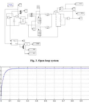
Fig. 3. Open loop system
Fig. 4. Output voltage 380V (DC)
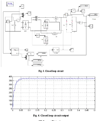
[image:6.595.147.443.443.786.2]Fig. 5. Closed loop circuit
Fig. 6. Closed loop circuit output
Passive PFC may be affected when environmental vibration occurs. Passive PFC requires that the AC input voltage be set manually. Passive PFC also does not use the full energy potential of the AC line.
Active PFC
The preferable type of PFC is Active Power Factor Correction (Active PFC) since it provides more efficient power frequency. Because Active PFC uses a circuit to correct power factor, Active PFC is able to generate a theoretical power factor of over 95%. Active Power Factor Correction also markedly diminishes total harmonics, automatically corrects for AC input voltage, and is capable of a full range of input voltage. Since Active PFC is the more complex method of Power Factor Correction, it is more expensive to produce an Active
PFC power supply
Simulation Design open loop
A simulation design open loop system as shown in Fig.3 is implemented in MATLAB SIMULINK with the help of coupled inductor, switches and diodes we get desired output voltage level (Fig.4)
Simulation Design closed loop
A simulation designopen loop system as shown in Fig.4.5 is implemented in MATLAB SIMULINK with the help of coupled inductor, switches and diodes we get desired output voltage level (Fig.4.6)
EXPECTED INPUT AND EXPECTED OUTPUT
Here the Input given to the circuit is 110V Vrms and the output got is 380V DC (high voltage)
Conclusion
ADVANTAGES
Improve power factor & power density.
Conduction losses & Switching losses are reduced.
Overall efficiency is improved.
Ripples are reduced.
APPLICATIONS
Medium power supplies.HEV (Hybrid Electrical Vehicles). UPS
FUTURE SCOPE
The system can be extended for more voltage range or levels. Increase in more levels wills sure increasing the voltage gain and efficiency of the converter system. The output DC can be use the high voltage applications.
REFERENCES
Akın, B. and Bodur, H. Feb. 2011. “A new single-phase soft-switching power factor correction converter,” IEEE Trans.
Power Electron., vol. 26, no. 2, pp. 436–443.
Chen, Y.T., Shiu, S. and Liang, R. Jan. 2012. “Analysis and design of a zero-voltage switching and zero-current-switching interleaved boost converter,” IEEE Trans. Power
Electron., vol. 27, no. 1, pp. 161–173.
Dwari, S. and Parsa, L. Jan. 2011. “An efficient high-step-up interleaved DC–DC converter with a common active clamp,” IEEE Trans. Power Electron., vol. 26, no. 1, pp. 66–78.
Hsia, T.H. Tsai, H.Y. Chen, D., Lee, M. and Huang, C.S. Jan. 2011.“Interleaved active-clamping converter with ZVS/ZCS features,” IEEE Trans. Power Electron., vol. 26, no. 1, pp. 29–37.
Hsieh, Y.C., Chen, M.R. and Cheng, H.L. Jan. 2011. “An interleaved flyback converter featured with zero-voltage transition,” IEEE Trans. Power Electron., vol. 26, no. 1, pp. 79–84.
Roh, Y.S., Moon, Y.J., Gong, J.C. and Yoo, C. Feb. 2011. “Active power factor correction (PFC) circuit with resistor-free zero-current detection,” IEEE Trans. Power Electron., vol. 26, no. 2, pp. 630–637.
Su, B., Zhang, J. and Lu, Z. Feb. 2011. “Totem-pole boost bridgeless PFC rectifier with simple zero-current detection and full-range ZVS operating at the boundary of DCM/CCM,” IEEE Trans. Power Electron., vol. 26, no. 2, pp. 427–435.
Yao, K., Ruan, X., Mao, X. and Ye, Z. Jan. 2012. “Reducing storage capacitor of a DCM boost PFC converter,” IEEE
Trans. Power Electron., vol. 27, no. 1, pp. 151–160.
Zhang, X. and Spencer, J.W. Dec. 2011. “Analysis of boost PFC converters operating in the discontinuous conduction mode,” IEEE Trans. Power Electron., vol. 26, no. 12, pp. 3621–3628.