Objectives:
1. Design and measure a 1.0 µH solenoidal air-core inductor 2. Analyze and build an audio microphone amplifier circuit.
3. Learn about the two conditions for oscillation in a feedback oscillator circuit. 4. Learn how to analyze a typical RF “LC” oscillator circuit.
5. Build/debug RF oscillator, then add audio modulation circuit to make a “wireless microphone”.
6. Experiment with radio wave propagation and different polarizations of radiated EM waves. Parts:
1. Q1 & Q2: two 2N3904 NPN BJTs 2. Cfdbk & Cx: two 22 pF capacitors 3. Ccoup & Cmic: two 0.1 µF capacitors
4. Cbypass1 & Cbypass2: two 0.001 µF (1 nF) capacitors 5. Rb2 & Rmic: two 10 kΩ resistors
6. Re2: one 1 kΩ resistor 7. Rb1: one 470 kΩ resistor 8. Rc1: one 560 Ω resistor 9. M1: one electret microphone
10. Lx: one 1.0 µH air-core, solenoidal inductor (+ or – 10%) (to be designed by the student using hookup wire)
Equipment:
1. Agilent triple dc power supply 2. Agilent Spectrum Analyzer
3. Agilent 0 – 100 MHz Digital Oscilloscope 4. Agilent 0 – 20 MHz Function Generator
[image:1.612.68.581.509.722.2]5. Portable FM radio (Walkman style or boom box style) 6. Tektronix Curve Tracer
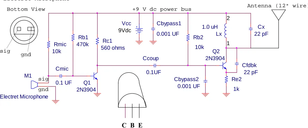
Figure 1. Complete Circuit of 34 MHz FM Wireless Microphone
+9 V dc power bus
Bottom View Antenna (12" wire)
M1
Electret Microphone
Electret Microphone
Q1 2N3904
sig gnd
Rb2 10k
Re2 1k Rc1
560 ohms Vcc
9Vdc
Cmic
0.1 UF
C B E
Q2 2N3904
gnd
Cx 22 pF Rb1
470k
sig
Ccoup
0.1UF
Cbypass2 0.001 UF Cbypass1 0.001 UF Rmic
10k
Lx 1.0 uH
1 2
1. Solenoidal air-core inductor
Design a 1.0 µH air-core solenoidal-wound (single-layer) inductor using the formula for self-inductance derived in class using a 0.4” diameter coil form or thereabout (such as a felt-tip marker pen) and regular insulated hookup wire. Recall that this inductance formula is:
l A N
L μ
2
= and in air μ= μ0 = 4π x 10-7 H/m
Use ordinary 24-gage or 22-gage insulated hookup wire that is “close-wound” on a coil form such as a pen. I suggest winding a 12-turn test coil on whatever form you have available, then after taking it off of the form, measure the cross sectional diameter, and calculate its area “A”. Note that “A” will expand after taking the coil off of the form. Once you measure “A” and the length of the coil, “l”, calculate the inductance of your test coil using the above formula, and then adjust the required number of turns in order to give you a result that is as close as possible to the required inductance of 1.0 µH.
Record your calculations in your lab notebook, and show your resulting design, indicating the resulting number of turns, cross-sectional area A, and the length of the coil, l. {Record}
Now measure your inductor by resonating it with a 1 nF = 0.001 µF capacitor. Note that the expected resonant frequency if L = 1.0 µH is 5 MHz, which is well within the frequency range of your function generator. Record the observed resonant frequency, and show your calculations of the true inductance of your inductor. {Record}
Because not all of the flux produced by each turn of the solenoidal-wound the coil will link (cut the surface of) each of the other turns in the coil, the formula derived in class will yield a high estimate of the true inductance. Therefore, you may have to add several turns to your inductor beyond what the formula predicts in order to realize the desired target inductance of 1.0 µH. If your measured inductance differs by more than plus or minus 10% from the target value, modify your design (change the number of turns) and try again, repeating the steps above until your inductor is at least within 10% of the target value. {Record}
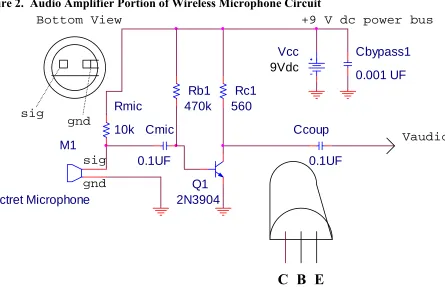
2. Audio microphone amplifier
Analyze the audio amplifier circuit of Fig. 2. Use the curve tracer to measure the β of the 2N3904 NPN BJT that you plan to use for Q1. You may assume that Vbe(on) = 0.7 V. From the dc model of the circuit, determine the quiescent base current, Ibq, and the Q-point of the BJT Q1 (Vce1q and Ic1q). Show your calculations in your lab book. {Record}
From this result, determine the dynamic resistance “rπ1” of the b-e junction of Q1 for small variations in Vbe about the given Q-point. {Record}
Recall that
bq T I V
rπ = where the thermal voltage VT =26 mV
Once rπ is determined, draw the ac small-signal model of this BJT audio amplifier in your lab book, and show that the small-signal (ac) voltage gain of the circuit is given by
Then calculate the numerical value of the voltage gain for your circuit. {Record}
Figure 2. Audio Amplifier Portion of Wireless Microphone Circuit
C B E
Ccoup
0.1UF
Vaudio sig
Rb1 470k
+9 V dc power bus
Vcc
9Vdc
sig
Rmic
10k
Rc1 560
Cmic
0.1UF
gnd Bottom View
Q1 2N3904 M1
Electret Microphone
Cbypass1
0.001 UF
gnd
Build this circuit, paying special attention to the microphone pinout and the transistor pinout shown above. Measure the voltage across Rc1 to determine Ic1q, and the voltage across the C and E terminals to measure Vce1q (compare your observed dc Q-point values with your calculated values above). {Record}
While someone hums or whistles at a constant volume into the microphone, measure the ac voltage gain by switching the oscilloscope input to “ac” coupled mode (to block out the dc voltage component of the signal) and then measuring the amplitude of the amplifier output voltage “Vaudio” and also the amplitude of the microphone voltage at the input of the amplifier (measured at the “sig” terminal of the Microphone M1). The ratio of these two voltages is the voltage gain. Compare your measured voltage gain with the voltage gain predicted above. (Calculate % deviation.) {Record}
3. Analysis of the Radio Frequency “LC”Oscillator Circuit
Use the curve tracer to measure the β of the 2N3904 BJT that you plan to use for Q2. Then predict the value of the dc quiescent operating point (Q-point) (Icq2 and Vceq2) in the oscillator circuit shown in Fig. 3. Show your work in your lab notebook. {Record}
C
Cx 22 pF ib2
B
beta2*ib2 rpi2
Cfdbk 22pF
Re2 1k E
Lx 1.0 uH
1 2
Figure 3. 34 MHz RF Oscillator Circuit
+9 V dc power bus
Re2
1k
Cfdbk 22 pF
Antenna (12" wire)
Cx 22 pF Cbypass1
0.001 UF Vcc
9Vdc
Q2 2N3904 Rb2
10k Lx 1.0 uH
1 2
Cbypass2 0.001 UF
We may construct the ac model of the RF oscillator circuit of Fig. 3 as shown in Fig. 4.
Figure 4. AC Model of RF Oscillator Circuit of Fig. 3
In this AC model, we have assumed that the two 0.001 µF capacitors, Cbypass1 and Cbypass2 act as short circuits at 34 MHz. This assumption is justified, since at a frequency of 34 MHz, the
impedance magnitude of a 0.001 µF capacitor is under 5 ohms! Note that 1/(2π*34 MHz*0.001 µF) = 4.82 Ω! Note that we do not want to pick the value of Cbypass2 to be much larger than this,
because we do NOT want it to keep the audio signal frequencies from our microphone amplifier from reaching the base of the RF oscillator transistor, where it is used to slightly vary the reverse bias voltage across the BC junction of our the oscillator stage back and forth at an audio rate.
A(f)
β
(f)
Amplifier Voltage Gain A(f)
Feedback Network Voltage Gain β(f)
=> Loop Gain = A(f)
β
(f)
via a frequency-selective feedback network that consists of Re2, Cfdbk, Lx, and Cx.
This feedback network completes a “feedback loop” that allows oscillations to build up only at a particular frequency “f”. This frequency of oscillation is primarily set by the parallel resonant tank circuit formed by Lx and Cx. Because admittances add in parallel, recall that this parallel resonant circuit exhibits the impedance
fLx j fCx j ZRxCx
π π
2 1 2
1 + =
This impedance becomes infinite (acts like an open circuit) when its denominator is set to zero. This occurs at the frequency where the positive imaginary capacitive admittance (which is increasing with frequency) cancels the negative imaginary inductive admittance (which is decreasing with
frequency).
0 2
1
2 + =
fLx j fCx j
π π
The frequency at which infinite impedance occurs is called the resonant frequency,
33.93
10 22 10 2
1 2
1
12 6 • × =
= =
− −
π
π LxCx
fres MHz
At frequencies below the resonant frequency “fres”, the right term in the denominator of the ZRxCx dominates, and the circuit exhibits a relatively low (inductive) impedance. Likewise at frequencies above the resonant frequency, the left term in the denominator of the ZRxCx expression dominates, and the circuit exhibits a relatively low (capacitive) impedance. Thus this circuit serves to divert to
ground signals of frequencies other than “fres”. Therefore, only noise at the frequencies near fres are passed around the feedback loop, allowing a significant oscillation to build up.
A general sinusoidal feedback oscillator consists of an amplifier and some sort of an external feedback network, as shown in Figure 5.
A(f)
β
(f)
Amplifier Voltage Gain A(f)
Feedback Network Voltage Gain β(f)
=> Loop Gain =
β
(f) A(f) = Vout/Vin
Vout
+
Vin-
Broken Feedback Loop
This general sinusoidal oscillator circuit of Fig. 5 will oscillate at a frequency “f” if and only if a
frequency “f” can be found that satisfies the following two conditions for oscillation, known as the “Barkhausen Conditions”:
(a) The magnitude of the voltage gain around the loop (loop gain) is greater than 1, so that noise at frequency “f” that is present due to the power-up transient will be amplified to higher and higher levels as it circulates around the frequency-
selective feedback loop. (The oscillations do not build up forever, since eventually the BJT is driven into saturation or cutoff. The oscillation amplitude is self-limiting due to inherent device nonlinearities.)
|A(f)β(f)| > 1.0
(b) The phase shift around the loop must be an integral multiple of 2π radians, so that
the fed back sinusoidal signal will add “in phase” (constructively) with the signal already at the input, and then oscillations can then build up.
Phase Angle [A(f)β(f)] = n2π, where n is any integer
The loop gain can be measured by breaking the feedback loop and inserting a sinusoidal test source on the input side of the break, then measuring the voltage gain around the loop, as shown in Figure 6
Figure 6. Breaking the Feedback Loop to Measure the Loop Gain
Cx 22 pF beta2*ib2 Vin(t) Vout(t) Cfdbk 22pF B E Lx 1.0 uH 1 2 ib2 C rpi2 Re2 1k
Figure 7. Breaking the Feedback Loop in the AC Model of Figure 4.
Write node equations at the emitter node (VE) and the collector node (Vout) in terms of the Laplace complex frequency variable “s”. Then eliminating VE, show that
]) ) 1 ( [ )( 1 ) ( ) ( ) ( 2 2 2 2 2 e e fdbk x x x x x x e fdbk R r r R sC R sC L C s R sL R sC s Vin s Vout LoopGain + + + + + + = = β β π π
If you use MAPLE to perform this derivation, which I highly recommend, please be sure to tape your MAPLE worksheet into your lab notebook. {Record}
Substitute the component values from Fig. 7 into the Loop Gain formula. Use the value of rπ2 that you calculated above. Also, let the series resistance of the inductor in the tank circuit,
Rx = 0.25 Ω.
Now replace s by j2πf, and use MAPLE to plot both the magnitude and phase of the loop gain for 30 MHz < f < 40 MHz. Your plots should look something like the ones I got, as shown in Figure 8. Note that at frequency at which the phase plot passes through 0 degrees, the magnitude of the loop gain is still well above unity, therefore the circuit will oscillate at this frequency. Note the frequency of oscillation is slightly higher than the resonant frequency of the tank circuit. Please be sure to tape your MAPLE plots, along with the marked frequency of oscillation into your lab notebook.
{Record}
Figure 8. Example Plots of Loop Gain Magnitude and Phase
4. Build/Debug/Test the FM Wireless Microphone!
Now build the RF oscillator circuit of Figure 1, keeping your leads as short as possible, as shown in the photograph of Figure 9. Temporarily remove Cfdbk to prevent the circuit from oscillating. Measure the dc Q-point of the RF oscillator transistor Q2 (Vce2 and Ic2 --- which is measured indirectly as the voltage across Re2 divided by Re2). Compare how closely this measured Q-point agrees with your predictions made earlier. (Calculate % deviation.) Note that we must stop Q2 from oscillating before we measure the dc Q-point, since our bench digital voltmeter is disturbed by the radio frequency oscillations!
Connect your oscilloscope to the output of the oscillator (Vout) at the collector of Q2. You should see a distorted sine wave whose frequency is close to what you predicted (around 34 MHz). If you do not see any oscillation, check your circuit carefully, and then see me!
Use the Quick Measure function of the oscilloscope to display the frequency of oscillation, the maximum voltage and the minimum voltage and then record this scope display picture and tape it into your lab notebook. {Record}
40 MHz
30 MHz 30 MHz 40 MHz
Loop Gain phase shift passes through 0 degrees at
Figure 9. Breadboarded Circuit of FM Wireless Microphone…
NOTE THAT YOU MUST KEEP ALL COMPONENT LEADS VERY SHORT!
Now use your spectrum analyzer to display the spectrum (from 0 to 500 MHz) of your wireless microphone, using a short (12”) length of wire as an antenna placed about one foot from your circuit board. Capture this screen and tape it into your lab notebook. How far down (in decibels) from the 34 MHz fundamental frequency the 2nd, 3rd, 4th harmonics lie? Indicate this in tabular form in your lab book. {Record}
Now listen to your wireless microphone on an FM radio. You may have to adjust the
frequency of your oscillator by pulling apart or compressing (slightly changing the inductance of) your 1 μH inductor in order to find a frequency that is not already being used on the FM radio band.
Note that the base of Q2 is at RF ground due to Cbypass2, but it is not at audio ground! Therefore the audio signal coupled into the base of the RF oscillator Q2 continuously varies the junction capacitance of the reverse biased B-C junction, changing the resonant frequency of the tank circuit (Lx – Cx) slightly, and thus the frequency of oscillation of the 34 MHz RF oscillator is varied back and forth at an audio rate. This results in FM modulation of the audio signal! Note that we may tune in this 34 MHz signal’s 3rd harmonic at 102 MHz on an FM receiver.
Investigate the range of your signal, and experiment with different orientations of the FM receiving antenna and the transmitting antenna. {Record}
Demonstrate your FM Wireless Microphone to the lab instructor, and obtain his verifying signature in your lab notebook. {Record}