A Basic Approach Towards EM and IR Analysis on
SOC
Smitha M R1, Swasti Pujari2, Amit Singh3, Mukul Anand4
1, 2, 3
Engineer, 4Technical Lead, Einfochips Ltd. (An Arrow Company)
Abstract: The gradual displacement of metal atoms in a semiconductor results into Electro migration, potentially causing open and shorts circuits such as void and hillocks. Clock nets are more prone to EM, as those are more frequently switched signals as compared to other nets. Because of this only, we avoid using highest drive strength clock buffers to build clock tree. The voltage drop in the metal wires constituting the power grid before it reaches the VDD pins of the standard cells called as IR drop. There are two types of IR drops - Static drop and Dynamic drop.
Keywords: Voids, Hillocks, IC Compiler-II, Apache Redhawk, Static IR, Dynamic IR.
I. INTRODUCTION
Electromigration occurs when the current density is high enough to cause the drift of metal ions in the direction of the electron flow and is characterized by the ion flux density. This density depends on the magnitude of forces that tend to hold the ions in place, i.e., the nature of the conductor, crystal size, interface and grain-boundary chemistry and the magnitude of forces that tend to dislodge them, including the current density, temperature and mechanical stresses.
Electromigration is the movement of metal ions forced due to an electric field, applied across a metal, as shown in Fig. 1. Ftotal = Fdirect + Fwind
Fdirect - Direct action of electric field on metal ions (represented in blue arrow)
[image:1.612.162.454.400.492.2]Fwind - Force on metal ions resulting from momentum transfer from the conduction electrons (represented in red arrow)
Fig.1.
Metal atoms travel toward the positive end of the conductor while vacancies move toward the negative end
II. EFFECTSOFELECTROMIGRATIONINMETALINTERCONNECTS:
Asymmetry in the ion flow results two different EM failure mechanisms. Outgoing ion flux exceeds the incoming ion flux results in an open circuit called as Voids as shown in Fig. 2 Incoming ion flux exceeds the outgoing ion flux results in a short circuit called as Hillock as shown in Fig. 3.
[image:1.612.142.482.593.713.2]III. PHYSICALDESIGNPARAMETERSEFFECTELECTROMIGRATION
A. Local current density
B. Homogeneity of the current flow
C. Current distribution within device pins
IV. METHODSTOFIXELECTROMIGRATION
A. Widen the wire to reduce current density
B. By keeping shorter wire length
C. Increasing the metal width
D. Downsizing the driver cells
E. Adding more Via’s
F. Layer switching is another option as upper metal layers in the technology have higher current driving capability (due to greater thickness)
1) Design Overview for all the experimental results for Signal EM and IR.
a) 1.2M Instance Count
b) 10 Macros
c) 650MHz Frequency
d) EDA Tools used ICCII, Apache Redhawk
e) PVT and Signoff Conditions
2) Static peak signal EM violation before fixing,
Number of violations 39 and worst EM ratio is 154.89mv as shown in Fig. 4.
3) After applying Double Width and Double Spacing (2W2S) NDR on violating nets,
Number of violations 0 and worst EM ratio is 0 as shown in Fig. 5.
Fig. 5. Applying Non-default rules
V. IRDROPANALYSIS
The Power supply in the chip is distributed uniformly through metal layers (VDD & VSS) across the design. These metal layers have finite amount of resistance. When voltage is applied to this metal wires current starts flowing through the metal layers and some voltage is dropped due to that resistance of metal wires and current. This drop is called as IR drop.
Types of IR drop
1) Static IR drop
2) Dynamic IR drop
VI. STATICIRDROPANALYSIS
In Static voltage drop, Instance will draw the current all the time, it does not matter when the instance switches. Independent of the cell switching, the drop is calculated with the help of wire resistance.
Calculates the average voltage drop of entire design assuming current drawn across is constant.
As average current is calculated this analysis depends on time period. This analysis is good for signoff checks in older technology.
A. Experimental Results for Static voltage drop.
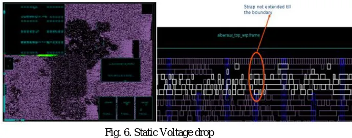
[image:3.612.133.490.98.225.2]There was voltage drop of 61.518mv in the design with 227 violating paths as power stripe is not extended till the boundary as shown in Fig. 6.
Fig. 6. Static Voltage drop
After extending the power stripe VSS till cell boundary, there was no voltage drop and hence no violating paths as shown in Fig. 7.
[image:3.612.156.500.467.602.2]VII. DYNAMICIRDROPANALYSIS
In Dynamic voltage drop, Instances will draw transient current only when it switches. Non-switching instance will draw only leakage current. Dynamic analysis will see the real peak demand current on the chip. Dynamic voltage drop depends on switching activity of the logic and is vector dependent. Less dependent on clock period as depends on instantaneous current.
[image:4.612.211.441.157.338.2]1) Experimental Results: There was voltage drop of 114.3mv with 17010 violating paths as shown in the Fig. 8.
Fig. 8. Dynamic Voltage drop
All Violations were resolved by using the below methods
a) Applied 50% Density screen on violating region.
b) Applied cell padding for FF.
VIII. METHODSTOREDUCEIRDROP
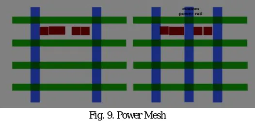
1) Robust Power Mesh: Initial power grid is made based on static IR analysis due to late availability of switching activity. If there is IR drop due to some of the clustered cells then adding a strip will make the power mesh more robust
Fig. 9. Power Mesh
2) De-cap: These are decoupling capacitors which are spread across the high switching region to maintain the voltage.
3) Spacing: If clock cells are clustered and causing IR drop, then by spacing those apart near to different power rails will reduce the IR drop. While shifting the cell to next power rail, make sure that the power rail is not driving many cells, because adding another cell may give IR drop.
4) Reducing Load: Cells driving more load will be drawing more current. Hence reducing load will reduce IR drop. 5) Downsizing: Cells of smaller size will draw less current. But the transition of cells should not become worse. 6) Increase the width of stripes. If width is already high, increase no of stripes.
7) Check if any via is missing and check if there is any scope to add more vias.
8) The number of power switches can be increased to reduce IR drop.
[image:4.612.175.438.453.578.2]IX. HOWIRDROPEFFECTSTHETIMING?
IR drop is signal integrity (SI) effect caused by wire resistance and current drawn off from power (Vdd) and ground (Vss) grids. According to ohms law, V=IR. If wire resistance is too high or the current passing through the metal layer is larger than the predicted, an unacceptable voltage drop may occur. Due to this unacceptable voltage drop, the power supply voltage decreases. That means the required power across the design is not reaching to the cells. This results in increased noise susceptibility and poor performance.
The design may have different types of gates with different voltage levels. As the voltage at gate decreased due to unacceptable voltage drop in supply voltage, the gate delays are increased non-linearly. This may lead to setup time and hold time violations depending on which path these gates are residing in the design.
As technology node shrinking, there is decreased in the geometries of the metal layers and the resistance of this wire increased which lead to decrease in power supply voltage during CTS, the buffers and inverters are added along the clock path to balance the skew. The voltage drop on the buffers and inverters of clock path will cause the delay in arrival of clock signal, resulting hold violation. Hold violations cannot be fixed once the chip is fabricated.
X. CONCLUSIONS
The EM and IR drop issues has been resolved by following the basic methods as used in the experiment mentioned above. The major challenge was developing a script for Redhawk violations integration in ICCII to highlight the EM/IR violations.
Future work can include merging the Redhawk inputs in the PnR stage to get an accurate estimation in the implementation stage and optimize accordingly.
XI. ACKNOWLEDGMENT
First and foremost, I would like to express my deepest gratitude to Jasmin Bhimani and AbbasAli Asamadi for their invaluable support throughout the period of this work.
REFERENCES
[1] J. Lienig, M. Thiele: "The Pressing Need for Electromigration-Aware Physical Design " (Proc. of the Int. Symposium on Physical Design (ISPD) 2018, pp. 144–151, March 2018
[2] Blech: Electromigration in Thin Aluminium Films on Titanium Nitride. Journal of Applied Physics, Vol 47, pp. 1203-1208 [3] https://www.ifte.de/books/em/em_chap2.pdf