Wireless Power Transfer for Mobile Charging
Applications
Girish Kumar1, Abhishek Kumar2, Kumar Shashant Shekhar3, Prashant Bajpai4, Under the guidance of Smt. Champa P.N.5
1, 2, 3, 4
Student, Department of Electrical and Electronics, B.N.M. Institute of Technology, Bangalore-560070, VTU, Belagavi, India.
5
Assistant Professor, Dept. of EEE, BNMIT
Abstract: The main objective of this project is to develop a device for wireless power transfer. The concept of wireless power transfer was realized by Nikolas Tesla. Wireless power transfer (WPT), wireless power transmission, wireless energy transmission or electromagnetic power transfer is the transmission of electrical energy without wires. Wireless
power transmission technologies use time-varying electric, magnetic, or electromagnetic fields. The basics of wireless power involves the transmission of energy from a transmitter to a receiver via an oscillating magnetic field. To achieve this, Direct Current (DC) supplied by a power source, is converted into high frequency Alternating Current (AC) by specially designed electronics built into the transmitter. Wireless Charging provides a convenient, safe, and reliable way to charge and power millions of electrical devices at home, in the workplace and in industry. From smartphones, electrical vehicles to hand-held industrial devices and heavy-duty equipment applications, wireless power maintains safe, continuous, and reliable transfer of power to ensure all varieties of devices and equipment are charged and ready to go at a moment’s notice. The limitations and challenges associated with the WPT techniques are explored.
I. INTRODUCTION
The wireless power transfer is the applications for the ability to transport power over great distances and the discussion of wireless power transmission as an alternative to transmission line power distribution started in the late 19th century. Both Heinrich Hertz and Nicolai Tesla theorized the possibility of wireless power transmission. Tesla demonstrated it in 1899 by powering fluorescent lamps 25 miles from the power source without using wires (1) Despite the novelty of Tesla’s demonstration and his personal efforts to commercialize wireless power transmission, he soon ran out of funding because it was much less expensive to lay copper than to build the equipment necessary to transmit power through radio waves boundaries without the need for transmission lines.
Loads using a high-frequency resonating air core transformer to develop the frequency from 50hz to 40 kHz for transferring power over a distance of 3cm wireless power transfer can make a remarkable change in the field of electrical which eliminates the usage of conventional copper cables and current carrying wires. Based on this concept, the project is developed to transfer the power within a small range. The patient is required to be operated every year to replace the battery. This project is built upon using an electronic circuit that converts ac 230v 50 Hz to ac 12v, high frequency. The output is fed to a tuned coil forming as primary of an air-core transformer. The secondary coil develops a voltage of hf 12volt. Thus, the transfer of power is done from the primary (transmitter) to the secondary, which is separated with a considerable distance. Therefore, the transfer could be seen as the primary transmission and the secondary receives the power to run the load.
The goal of the project was to evaluate and study the wireless power transfer technologies and physics behind it. The design and implementation of the wireless energy transmission system prototype and its implementation in the next floor innovative floor was the main plan. It was crucial for next floor to integrate advanced technologies into their floor system in order to make it really “smart” and innovative and wireless power transfer was one of them. WPT is a very broad though relatively new technology – almost 80% of references are dated later than the year 2010; hence, the scope of the project was limited to implementation of the inductive power transfer mode.
A. Main Concepts Of Wireless Transmission Of Electric Energy
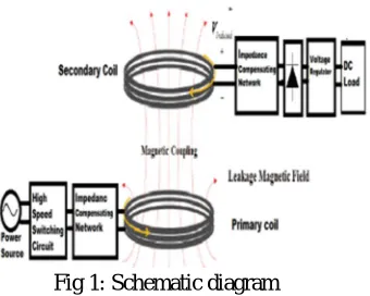
B. Schematic diagram
Fig 1: Schematic diagram
The high speed switching circuit is a single-ended high frequency quasi resonant inverter that consists of power MOSFETs and triggering circuits. A power MOSFET is a Metal Oxide Semiconductor Field Effect Transistor (MOSFET) designed to handle significant power levels and can operate at high frequencies up to hundreds of kilo Hertz. Now, the power electronics development reaches to a new power MOSFET (SiC MOSFET) that can operate at frequencies up to Mega Hertz which is used for high switching frequency applications. The impedance compensating network (matching network) has a very important role in WPT system .It reduces the volt-ampere rating of the power source by minimizing the reactance of input impedance and increase the power transfer efficiency by utilizing the magnetic field resonance. The time varying magnetic field is generated from the primary coil and is gathered at the secondary coil to transfer the average load power. There are two lose contributions associated with the diodes in a high frequent rectifier; losses due to the forward conduction of the diodes and the high frequent loss according to the switching time of the diodes. These losses act as a consequence of the reverse recovery time of the diodes. To eliminate the loss effect, Schottky diodes or ultrafast diodes are used in the rectifier circuit instead of normal diodes. The voltage regulator is used to stabilize and control the DC voltage level according to the required load voltage. The mobile battery is a common load in a WPT system as charging a mobile wirelessly means no need to connect the mobile charger to a mobile phone. The mobile phone is put on the charging pad and the charging operation starts till the phone is fully charged.
II. A STUDY ON INDUCTIVE CHARGING COIL
Michael Faraday and Joseph Henry are the prime individual’s in the discovery of Electromagnetic induction. In 1831 Faraday publishing his study on inductive charging coil becoming the main official person of this Phenomenon. He demonstrated his experiment by wrapping two wires opposite to an iron torus, with one wire into the galvanometer, and another to battery terminals, he observed a transient current which he named as wave of electricity while connecting and disconnecting the wire from battery. Henry's demonstration was based on an electromagnet perched on a pole, rocking back and forth. The rocking motion was caused by one of the two leads connected to both ends of the magnet rocker, touching one of two battery cells causing a polarity change. It kept rocking in the opposite direction until the other two leads hit the other battery. This demonstration allowed Henry to recognize the property of self-inductance. Then James clerk Maxwell came with his classical electromagnetic theory. In which he related all previously unrelated observations, equation and experiments. Later by Oliver Heaviside brought down this to four famous equations known as the Maxwell’s equation. Heinrich Rudolf Hertz proved this Electromagnetic theory by engineering instruments. And in 1891 Nikola Tesla demonstrated wireless transmission of energy which was based on Michael Faraday electromagnetic theorem.
A. Inductive Charging Theory
Inductive charging by induction principle is based on the theory given by Maxwell’s equation. Current flowing through any conductor produces a magnetic field, variation in the magnetic field creates an electric field and this electric field causes the electrical charge to move there by producing a current.
sE.ds= Q
0 .
sBds
……...……...… (2)
dt d dl E b c
. ………...… (3)
) (
. 0 0
dt d I dl B e c
.... (4)
According to equation (4) a magnetic field is created in closed loop by current running through it and known as magnetic flux density, B. hence there flows a magnetic flux ΦB, henceforth called Φ.
SBdS
B .
………...…... (5)
LI
………... (6)
If we Place a second closed loop in the domain of the first then it cause some of the magnetic flux from first loop, due to B1, to pass
through the surface of the second loop, S2. This is designated as the mutual flux Φ12.
2 1 2
12 SB.dS
……...….... (7)
1 2 1
21 SB.dS
……... (8)
The proportionality coefficient between the current and the mutual flux is the mutual inductance. Mutual inductances are the same.
1 12 12L I
……... (9)
2 21 21L I
……... (10)
21 12 L L
M ……... (11)
B. The Coils
The coils are used to give a path for current to flow through a closed loop and if it has N number of turns, the current in every turn will be added to magnetic flux density (B), where B is proportional to number of turns carrying current I.
NI
B …………... (12)
(fluxlinkage)N ... (13)
I
L... (114
The self-inductance is proportional to the square of the number of turns of the coil.
2 N
L ... (15)
Mutual inductance is due to current I1 flowing through a coil with N1 turns, causing a magnetic flux density B1.
1 1 1 NI
B ... (16)
The mutual inductance is calculated through flux linkage .
1 12 I
M ... (17)
Where,
12 2 12
N ... (18)
2 1 12B.dS
... (19)
Where,
1 1I N
B ... (20)
2 1N N
The ratio between the mutual inductance and self-inductance is given by equation (22).
2 1L L k
M ... (22)
The magnetic coupling between the coils is independent of Number of turns in the coils and only depends on the positions of the two coils and the physical properties of the media.
C. Mutual Inductance
An alternating flux linkage to a coil will cause an induced electromotive force, or voltage.
dt t D t
U2() 12() ... (23)
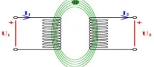
[image:4.612.228.387.255.324.2]Current flowing through coil1 produces magnetic field and hence a magnetic flux through coil 2. If current in coil 1changes the flux through coil 2 changes as well. Like this a change in current in one circuit can induced a current in a second circuit this phenomenon is known as “mutual induction”. This phenomenon can be understood clearly from figure 2. Like the self-inductance (L), two circuits have mutual inductance (M) also.
Fig: 2: Representing mutual inductance
Current I1 flows through the main coil and causes a voltage V2 in the second coil. If the second coil is closed, a current I2 will flow
in it. This current will setup the magnetic flux density B2, which causes a magnetic flux. Figure 3 represents equivalent circuit
diagram of mutual inductance.
Let Ψ22 is Self-flux linkage and Ψ12 is mutual flux linkage, then
) ( ) ( )
( 12 22
2 t t t
... (24)
) ( ) ( )
( 11 21
1t t t
... (25)
In terms of inductance
) ( ) ( )
( 11 2
1 t Li t Mi t
... (26)
) ( ) ( )
( 1 22
2 t Mi t Li t
... (27)
Relationship between input voltage, current and output voltage, current is given by
dt t Mdi tdt di L t
U1 1 1 2() .. (28)
tdt di L dt t Mdi t
U1 1() 2 2 ..(29)
Fig 3: Equivalent circuit diagram of mutual inductance
III. HARDWARE REQUIREMENT
A. PIC Microcontroller
Peripheral Interface Controllers (PIC) is one of the advanced microcontrollers developed by microchip technologies. These microcontrollers are widely used in modern electronics applications. A PIC controller integrates all type of advanced interfacing ports and memory modules. These controllers are more advanced than normal microcontroller like INTEL 8051.
Fig 4: Pin diagram 16C72
[image:5.612.216.398.287.429.2]B. Battery: The rechargeable batteries used are lead-lead dioxide systems. The dilute sulfuric acid electrolyte is absorbed by separators and plates and thus immobilized. Should the battery be accidentally overcharged producing hydrogen and oxygen, special one-way valves allow the gases to escape thus avoiding excessive pressure build-up. Otherwise, the battery is completely sealed and is, therefore, maintenance-free, leak proof and usable in any position.
Fig 5: Battery
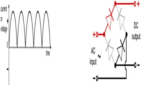
C. Bridge Rectifier
A bridge rectifier can be made using four individual diodes, but it is also available in special packages containing the four diodes required. It is called a full-wave rectifier because it uses the entire AC wave (both positive and negative sections). 1.4V is used up in the bridge rectifier because each diode uses 0.7V when conducting and there are always two diodes conducting, as shown in the diagram below. Bridge rectifiers are rated by the maximum current they can pass and the maximum reverse voltage they
canwithstand (this must be at least thee times the supply RMS voltage so the rectifier can withstand the
peak voltages).
[image:5.612.95.339.557.704.2]Alternate pairs of diodes conduct, changing over the connections so the alternating directions of AC are converted to the one direction of DC.
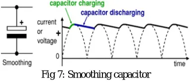
D. Smoothing Capacitor
[image:6.612.210.401.192.275.2]Smoothing is performed by a large value electrolytic capacitor connected across the DC supply to act as a reservoir, supplying current to the output when the varying DC voltage from the rectifier is falling. The diagram shows the unsmoothed varying DC (dotted line) and the smoothed DC (solid line). The capacitor charges quickly near the peak of the varying DC, and then discharges as it supplies current to the output.
Fig 7: Smoothing capacitor
E. Regulator
Voltage regulator ICs are available with fixed or variable output voltages. They are also rated by the maximum current they can pass. Negative voltage regulators are available, mainly for use in dual supplies.
The LM78XX series of three terminal regulators is available with several fixed output voltages making them useful in a wide range of applications. One of these is local on card regulation, eliminating the distribution problems associated with single point regulation. The voltages available allow these regulators to be used in logic systems, instrumentation, HiFi, and other solid state electronic equipment. Although designed primarily as fixed voltage regulators these devices can be used with external components to obtain adjustable voltages and current. Many of the fixed voltage regulator ICs has 3 leads and look like power transistors, such as the 7805 (+5V 1A regulator). They include a hole for attaching a heat sink if necessary.
Fig 8: Connection for regulator
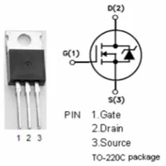
F. Mosfet (IRFZ44N)
Designed for low voltage, high speed switching applications in power supplies, converters and power motor controls, these devices are particularly well suited for bridge circuits where diode speed and commutating safe operating areas are critical and offer additional safety margin against unexpected voltage transients.
1) Id = 49A
2) Vgs = 20V
[image:6.612.213.402.435.602.2]Fig 9: Mosfet
G. Boost Converter
A boost converter (step-up converter) is a DC-to-DC power converter that steps up voltage (while stepping down current) from its input (supply) to its output (load). It is a class of switched-mode power supply (SMPS) containing at least two semiconductors (a diode and a transistor) and at least one energy storage element: a capacitor, inductor, or the two in combination. To reduce voltage ripple, filters made of capacitors (sometimes in combination with inductors) are normally added to such a converter's output (load-side filter) and input (supply-side filter). The key principle that drives the boost converter is the tendency of an inductor to resist changes in current by creating and destroying a magnetic field. In a boost converter, the output voltage is always higher than the input voltage.
L S S
f D V L
min ….………... (30)
Fig 10: Boost convertor
H. Dc to ac inverter
A power inverter, or inverter, is an electronic device or circuitry that changes direct current (DC) to alternating current (AC). The input voltage, output voltage and frequency, and overall power handling depend on the design of the specific device or circuitry. The inverter does not produce any power; the power is provided by the DC source. A power inverter can be entirely electronic or may be a combination of mechanical effects (such as a rotary apparatus) and electronic circuitry. Static inverters do not use moving parts in the conversion process.
I. Coil specification
.. (31)
where, N = no. of turns
u0 = permeability of free space
ur = relative permeability
D = loop diameter
d = wire di 8 ) 2]
[ln( ) 2 (
0 2
d D D
N
[image:7.612.223.419.360.488.2]Table 1: Coil specifications Transmitter
coil
No. of turns 20
Dia. Of each turn 10cm
Dia. Of Copper wire
.8mm
Inductance 123uH
Receiver coil
No. of turns 80
Dia. Of each turn 7cm
Dia. Of Copper wire
.3mm
Inductance 1.5mH
IV. HARDWARE SET UP
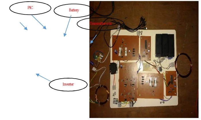
A. DC input (Battery)
For the supply, a DC input is taken. The battery provides a portable means of power source. 4V, 1.0Ah battery is taken for the purpose and such 6 batteries are connected in such a combination, to provide 12V. The first three batteries are connected in series and another three in series, and these combinations are then connected in parallel. These batteries also provide a means of recharging, which can be through solar panels.
Fig 11: Hardware set up for the WPT
B. Boost convertor
To get the desired voltage output for mobile charging purpose, the dc voltage has to be boosted to a higher level with a Boost convertor circuit. The dc voltage is boosted up to around 60V. The switches used are Mosfets, which are controlled by a PIC.
C. PIC
The PIC 16c72 is used here to control the Mosfets, the switching frequency is 1MHz. The supply to PIC is through the same battery. It has a voltage regulator, to limit the voltage to ICs required voltage input.
D. Inverter
After boosting the dc voltage up to 60V, for transmission through the coils, we require an ac signal, so the dc is converted to ac by an inverter circuit. The H-bridge of Mosfets are used to invert the dc into an ac. The Mosfets are triggered through PIC.
E. Regulator
Since the ac level is too high, Mosfets are provided with heat sinks and also it is needed to be stepped down to a lower level. So, the ac is stepped down to 9V.
Transmitter coil Battery
[image:8.612.56.405.326.535.2]F. Coils
[image:9.612.41.402.150.290.2]There are two coils for transmission, called as the transmitter and receiver coils. The transmitter is fed the ac input, the current through this coil produces a magnetic flux. This flux links with the receiver coil and a current is induced in receiver coil. Since there is no electrical contact between the coils through any wire, hence there is a wireless power transmission. The power transmission between the coils is taking through a magnetic circuit.
Fig 12: Transmitter and receiver coils
G. C-filter
The current in the receiver coil has to be filtered through a C-filter, to get the required frequency for the charger as well as to eliminate the harmonics and ripples.
H. Mobile Charger
The filtered output is provided to the charger, for the charging purpose. Multiple outputs and sockets can be provided for charging of multiple devices at the same time, a standard mobile charger can be used directly.
[image:9.612.132.404.402.544.2]V. EXPERIMENTAL RESULTS
Fig 13: Dc input of 12V from battery
The rechargeable batteries are lead-lead dioxide. The dilute sulfuric acid electrolyte. And a voltage of 12V is applied through a combination of 6 batteries to the boost convertor circuit.
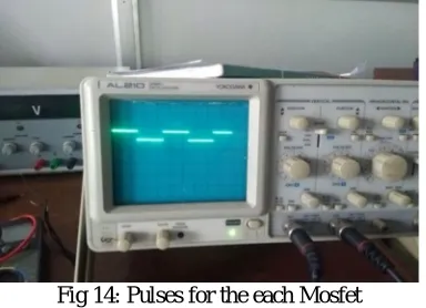
Fig 14: Pulses for the each Mosfet
The pulse obtained from the PIC is of 50% duty cycle. It is given to each of the Mosfets with a switching frequency of 1MHz.
Transmitter coil Receiver coil
Mobile phone
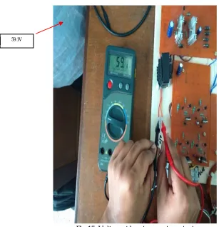
[image:9.612.212.404.579.718.2]Fig 15: Voltage at boost converter output
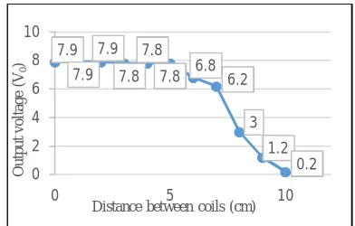
Table 2: Output voltage obtained at different coil distances. Distance
between coils (cm)
Input voltage (Vin)
Output voltage (V0)
0 - 1.5 9 7.9
1.5 - 2.5 9 7.9
2.5 - 3.5 9 7.8
4 – 4.5 9 7.8
5 9 7.8
5.5 9 7.7
6 9 6.8
6.5 9 6.2
7 9 6.2
7.5 9 3.2
8 9 3
8.5 9 2.5
9 9 1.2
9.5 9 .4
10 9 .2
Fig 16: Graph of output voltage vs different distance between coils
Table 3: V0/Vin for different coil distances
Distance between coils (in cm)
V0/Vin (in %)
0 - 2.5 87.0
2.5 - 3.5 87.0
3.5 - 4.5 86.6
4.5 – 5.5 86.6
6 75.5
6.5 68.8
7 68.8
7.5 35.5
8 33.3
8.5 27.7
9 13.3
9.5 4.4
10 2.2
Fig 17: Graph of V0/Vin vs different distance between coils
VI. CONCLUSION
Wireless power transfer using inductive coupling is much associated in terms of distance between coils and the range of frequency, resulting in higher power transfer with lesser distance. Based on experimental result, for optimum output voltage, the distance that the power can be transmitted is up to 5.0-6.5 cm with around 5 Volts, which can be supplied to the mobile phone charger. Also the maximum distance that the power can be transmitted is up to 8 cm with 3.0 Volts, because of this condition, the mobile phone still can be charged. It can also be seen that the wireless power transfer is not much affected by shielding materials such as the presence of hands, books and types of plastics. The result shows that the wireless powers transfer is suitable to be implemented for mobile phone charging applications.
7.9 7.9
7.9 7.8
7.8
7.8 6.8 6.2
3 1.2 0.2 0 2 4 6 8 10
0 5 10
O u tp u t v o lt a g e (V 0 )
Distance between coils (cm)
87 87 87 86.6 86.6 86.6 75.5 68.8 33.3 13.3 2.2 0 20 40 60 80 100
0 5 10
V0
/V
in
(%
)
VII. FUTURE WORK
To transmit the power to a greater distance, a high power radio frequency amplifier connected with an oscillator is needed. But the construction of the bulky RF power amplifier requires much time and patience. High power vacuum tube transistor amplifier with high current will make the system more efficient. A crystal oscillator circuit might be a better option for the transmitter circuit since it can produce a very high frequency A.C. current. Further effort on this same project can yield some real solutions that can solve the problems of this project. The knowledge of this project will help those who want to design a wireless charging system.
REFERENCES
[1] HongZhou, BinZhu, WenshanHu, ZhiweiLiu, XingranGao “Modelling and Practical Implementation of 2-Coil Wireless Power Transfer Systems”. Department of Automation, School of Power and Mechanical Engineering, Wuhan University, Wuhan 430072, China [Published 3 September 2014].
[2] Tawfikur Rahman, S.M.A. Motakabber and M.I. Ibrahimy, “Design of a Switching Mode Three Phase Inverter”. Departement of Electrical and Computer Engineering, International Islamic University Malaysia, Kuala Lumpur, Malaysia [2016 International Conference].
[3] Syed Khalid Rahman, Omar Ahmed, Md. Saiful Islam, A. H. M. Rafiul Awal, Md. Shariful Islam “Design and construction of wireless power transfer system using magnetic resonant coupling”. Department of Electrical & Electronic Engineering, World University of Bangladesh, Dhaka, Bangladesh [Vol. 2, No. 2, 2014].
[4] J.P.K. Sampath, A.Alphones, Hitoshi Shimasaki, “Coil design Guidelines for High Efficiency of Wireless Power Transfer(WPT)”. School of Electrical and Electronic Engineering, Nayang Technological Universit, Singapore [2016 IEEE].