A High Breakdown Voltage Two Zone Step Doped Lateral Bipolar Transistor on
Buried Oxide Thick Step
Sajad A. Loan, S. Qureshi and S. Sundar Kumar Iyer
Abstract----A novel two zone step doped (TZSD) lateral bipolar junction transistor (LBJT) on silicon-on-insulator (SOI) with buried oxide thick step (BOTS) is proposed. The concept of linear doping and linear oxide thickness for increasing the breakdown voltage has been replaced by using step in doping and step in oxide thickness. These steps result in the creation of additional electric field peaks in the collector drift region and increases the uniformity of lateral surface electric field and hence the breakdown voltage. Numerical simulations demonstrate that the breakdown voltage of the proposed device is more than 200 % higher than the conventional device
Index Terms----Silicon-on-Insulator, Lateral bipolar junction transistor, Breakdown voltage.
I. INTRODUCTION
The SOI-BiCMOS is emerging as a promising technology for realization of wireless system-on-chip. This technology offers advantages in terms of reduction of parasitic capacitance, high quality isolation and reduction in crosstalk [1]. However, the problem of compatibility lies in the integration of vertical bipolar device with SOI-CMOS [2]. This problem has been reduced by using lateral bipolar device as an alternative to the vertical device. The lateral bipolar junction transistor (LBJT) offers low parasitic capacitance, promises low power consumption and high breakdown voltage.
To obtain the large breakdown voltage, the lateral surface electric field distribution along the silicon surface must be uniform [3]. Several ideas have been used to enhance the breakdown voltage of the lateral bipolar devices. These include Reduced Surface Field (RESURF) principle [4], fully depleted collector drift region [5], graded drift region [6], [7], semi insulating polysilicon (SIPOS) passivation layers [8]. The concept of extended box has been used to increase the breakdown voltage of lateral Schottkey transistor [9].
By using linearly varying doping concentration and linearly varying oxide thickness, the lateral surface component of the electric field in the device can be made uniform, and the breakdown voltage can be enhanced.
The authors are with the Department of Electrical Engineering, Indian Institute of Technology Kanpur, Kanpur-208016, India, E-mail: (sajad@iitk.ac.in).
But it is extremely difficult to fabricate a device with linearly varying doping concentration and simultaneously having linearly varying oxide thickness [10-12].
In this paper, numerical simulation of LBJT with two zone step doped (TZSD) drift region on buried oxide thick step (BOTS) has been performed. To increase the breakdown voltage and at the same time retain the ease of fabrication of the device, the linearly varying doping and the linearly varying oxide thickness has been replaced with step profile of both. The two zone step doping and thick step oxide results in increased uniformity in the lateral electric field in the drift region, reduction of base-collector junction electric field by using lower doping concentration near the junction and enhancement of collector breakdown voltage. The simulation results using MEDICI [13] has shown that the proposed device has breakdown voltage of more than 200 % higher than the conventional device, that is, TZSD device without BOTS
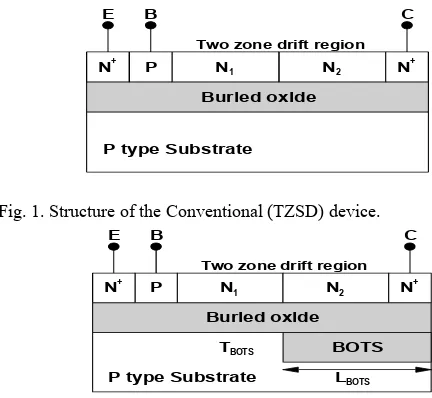
II. DEVICE STRUCTURE
The structures of the conventional and the proposed device are shown in Fig. 1 and Fig. 2 respectively. The n type emitter/collector doping concentration is 5 × 1019 cm-3. The drift region consists of two zones N
1 and N2
of n type doping concentration of n1 = 3 × 1015 cm-3 and n2 =
5 × 1015 cm-3 respectively. The p type substrate and base
doping concentration is 5 x 1013 cm-3 and 5 x 1016 cm-3 respectively
.
The oxide is 1.5 μm thick and the thickness of BOTS is varied from 1 μm to 6 μm.Buried oxide
E B C
N2 N
+
P type Substrate N1
P
Two zone drift region
[image:1.612.321.537.526.725.2]N+
Fig. 1. Structure of the Conventional (TZSD) device.
E B C
N1 N2 N
+
P N+
Two zone drift region
Buried oxide
P type Substrate BOTS TBOTS
LBOTS
III. SIMULATION RESULTS
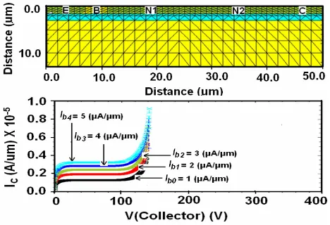
[image:2.612.61.295.153.313.2]Fig. 3 and Fig. 4 show the structures of the conventional and proposed device generated by MEDICI. These figures also show the output characteristics of these devices for various values of base currents.
Fig. 3. Output characteristics of conventional device.
[image:2.612.59.294.342.512.2]
Fig. 4. Output characteristics of the proposed device.
The simulation results have shown that the common emitter breakdown voltage with base open (BVCEO)
is significantly higher for the proposed structure than the conventional device. For the proposed device with BOTS length of 18 μm and thickness of 6 μm, the BVCEO is 290 V.
The BVCEO of the conventional device is 124 V. The reason
behind this enhancement in breakdown voltage is explained in Fig. 5, which shows that the lateral surface electric field is more uniform in the proposed structure than in the conventional device. The enhanced uniformity in surface electric field is due to the presence of step in doping and step in oxide [10]. These steps result in the generation of additional electric peaks in the collector drift region, which are shown in Fig. 5. These generated peaks pull down the peaks at the edges of the collector drift region. Further, the thick step oxide reduces the peak electric field at n2-n+
junction by redistributing applied potential in the collecto
drift region and in thick oxide. The analytical approach deduced in [12] explains the creation of the electric field component due to BOTS and increase in breakdown voltage.
r
e in proposed and conventional
he potential contours of the conventional and the proposed
ig. 6. Potential contours in the conventional device.
ig. 7. Potential contours in the proposed device.
ectric field ofiles
Fig. 5. Electric field profil devices.
T
devices are shown in Fig. 6 and Fig 7 respectively. The crowding of the potential contours along the oxide layer as shown in Fig. 6, results in lowering the breakdown voltage in the conventional device. In the proposed device, BOTS helps in reducing the crowding of the potential contours as shown in Fig. 7. This reduction in crowding of the potential contours in BOTS, makes it possible to apply more voltage to the device before it breaksdown.
F
F
Fig. 8(a) and Fig. 8(b) show the el
[image:2.612.319.567.448.529.2] [image:2.612.320.574.566.648.2]device that the BOTS length of 36 um gives maximum breakdown voltage of ~400 V for specific values of doping concentration in different regions and a specific BOTS thickness. The increase in breakdown voltage can be attributed to how the electric field peaks are distributed in the device for different values of BOTS length.
(a)
(c)
ig. 8. Electric field profi he proposed device at (a) p (b) bottom of silicon film (c) inside the oxide layer for different values of L(BOTS).
ptimum length of the BOTS is neede
(b)
le in t F
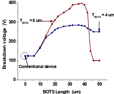
[image:3.612.349.534.187.339.2]to
Fig. 9 gives the breakdown voltage versus BOTS length characteristics of the proposed device. It is quite obvious from the plot that an o
d to get the maximum breakdown voltage. From this plot it is clear that for the BOTS length of 25 um to 40 um, the breakdown voltage is more than three times (for TBOTS = 6 um) and more than two times (for TBOTS = 4 um)
that of the conventional device.
0 10 20 30 40 50
0 100 200 300 400
TBOTS = 6 um
Br
eakd
o
w
n
vo
ltag
e (
V
)
BOTS Length (um)
TBOTS = 4 um
Conventional device
Fig. 9. Breakdown voltage versus BOTS length.
The impact of oxide thickness on breakd wn breakdown oltage first increases with increase in BOTS thickness, then sub
o voltage is shown in Fig. 10. It shows that the v
sequently saturates. This is because thick BOTS helps to sustain high electric field to a value lower than the field causing breakdown in the oxide. Since both horizontal and vertical components of the electric field contribute to the avalanche process, increasing BOTS thickness further does not improve breakdown voltage [9]. The simulation results have shown that for TBOTS = 6 um and LBOTS = 36 μm, the breakdown voltage of the proposed device is ~400 V and that of the conventional device is 124 V. This shows that the breakdown voltage in the proposed device is enhanced by ~223 %.
0 1 2 3 4 5 6 7 8
0 100 200 300 400
Br
e
a
k
dow
n Vol
ta
g
e (
V
)
Thickness of BOTS (um) BOTS length = 32 um
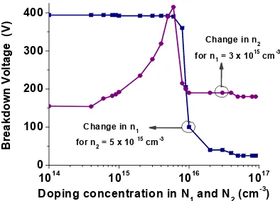
Fig. 11 shows the effect of substrate doping on the breakdown voltage. It is observed that there is an optimum doping concentration which gives the maximum breakdown voltage. The effect is explained in Fig. 12, which shows electric field profile at specified values of substrate doping. At high substrate doping concentration, the electric field builds up at the n2-n+ junction. This electric field peak
breaksdown the device at low voltage. At low substrate doping, the electric field builds up at the collector base junction, and ultimately breakdown occurs due to this
electric field peak. 01014 1015 1016 1017
100 200 300 400
Change in n1
for n2 = 5 x 10 15
cm-3
Bre
a
kdown
Vo
lt
ag
e
(
V
)
Doping concentration in N1 and N2 (cm-3
)
[image:4.612.73.271.234.380.2]Change in n2 for n1 = 3 x 1015 cm-3
Fig. 13. Breakdown voltage versus drift doping concentration in N1 and N2.
1014 1015 1016 1017
0 100 200 00 3 400
Proposed device
Brea
k
down V
olta
Doping concentration in substrate (cm-3)
(V
)
g
e
[image:4.612.320.564.381.553.2]Conventional device
Fig. 11. Breakdown vo
TBOTS = 6 um
ltage versus substrate doping concentration.
Fig. 12. Electric field profile at specified values of substrate doping concentration.
Fig. 13 shows the effect of varying doping concentration in the two zones of drift region on breakdown voltage. It is clear that there are optimum values of drift region doping concentration in the two zones, which gives maximum breakdown voltage. The optimum drift region doping concentration in N1 and N2 is about 6 x 1015 cm-3.
LBOTS = 32 um
The electric field profile at specified values of doping concentration in two zones N1 and N2 is shown in
g 14. For n = 3 x 1016 cm-3, the electric field at
collector-base jun
Fig. 14.
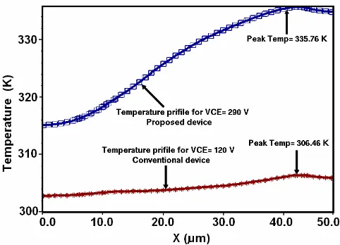
d device it rises to 335.76 K, when operated at its breakdown voltage of 290 V. The reason behind this temperature enhancement is the presence of thick oxide under collector and operation at high voltage. However, as the breakdown voltage does not increase continuously with increase in oxide thickness, temperature
Fi 1
ction is high and results in breaking down the device at 40 V. Similarly, at the doping concentration of n2
= 7 x 1016 cm-3, the electric field peak shifts to n
2-n+
junction and hence breaksdown the device at 180 V. The electric field profile is more uniform for optimum values of
n1= n2 = 6 x 1015 cm -3.
Electric field profile at specified values of drift doping concentration in the proposed device.
[image:4.612.59.296.417.600.2]of the device can be kept in safe region by choosing optimum oxide thickness.
Fig. 15. Temperature profile of the proposed and conventional devices.
VI. CONCLUSION
Numerical simulation of a novel lateral bipolar junction transistor on SOI has been performed. The novelty in the device is the combination of two zone step doping with the thick step oxide. It is known that the linearly varying drift doping and linearly varying oxide thickness results in maximum breakdown voltage. However, it is very difficult to fabricate such a device. In this paper a device with high reakdown voltage and relatively easy to fabricate has been roposed. The BVCEO has beenmaximized by choosing
appropriate values of TBOTS and LBOTS. The breakdown
voltage has been found to be dependent on substrate doping and drift region doping concentration. In this simulation study a more than 200 % increase in breakdown voltage has been observed.
ACKNOWLEDGMENT
The authors would like to thank the Ministry of Communication and Information Technology, Govt. of India, New Delhi, for their support, which made this work possible.
ng and B.j.Baliga, “Extention of resurf principle to die
the on Power
Semiconductor Devices and ICs. pp. 27-30, April 1991.
. Zhang, J. K. O. Sin, T. M. L. Lai, and P. K. KO, “Numerical modeling of linear doping profiles for high-voltage think film SOIdevices,” IEEE Transactions on Electron Devices, vol. 46, no. 5, pp.1036-1041, 1999. [7] G.J. Cao, M. M. De Soza, and E. M. S. Narayanan,
“Resurfed Lateral Bipolar Transistor for High-Voltage, High-Frequency Applications.” Proceedings of the 12th International Symposium on Power Semiconductor
Devices and IC 7. May
2000
[8] D. Jaume, G. Charitat, J. M. Reynes. and P. Rossel,
[11]
b
p
REFERENCES
[1] T.H.Ning, “Why BiCMOS and SOI BiCMOS” IBM Journal of Res & Dev, vol 46, no 2/3, Mar /May2002. [2] I-Shun Michael Sun et. al, “Lateral High speed Bipolar
transistors on SOI for RF SoC applications” IEEE Transactions on Electron Decives, vol 52, no.7, July 2005.
[3] S.D. Roy and M.J. Kumar, “Realizing High Voltage Thin Film Lateral Bipolar Transistors on SOI with a Collector Tub” Microelectronics International, 22/1, pp 3-9, 2005. [4] Y.S.Hua
lectrically isolated power devices,” Proceedings of 3rd International Symposium
[5] M. J. Kumar and K. N. Bhat, ”Collector recombination lifetime from the quasi-saturation analysis of high voltage bipolar transistors,” IEEE Trans. on Electron Devices, vol. 37, no. 11, pp. 172-177, 1995.
[6] S
s. Toulouse, France, pp. 185-18
“High-Voltage planar devices using filed plate and semi-resistive layers,” IEEE Tram. on Electron Devices, vol. 38, no. 7, pp.1478-1483, July1991.
[9] Kumar M.J and Roy S.D, “A New High Breakdown Voltage Lateral Schottkey Collector Bipolar transistor on SOI: Design and Analysis” IEEE transactions Electron Device, vol 52, no. 11 Nov. 2005.
[10] R. Sunkavalli et. al, “Step drift doping profile for high voltage DI lateral power devices” Proceedings of IEEE International SOI Conference, pp. 139-140, Oct. 1995 2005.
J.Luo et al, “A high performance RF LDMOSFET in thin film SOI technology with step drift profile”, Solid State Electronics 47(2003) 1937-1941.
[12] I.J.Kim, et.al, “Breakdown Voltage improvement for thin film SOI Power MOSFET’s by a Buried Oxide Step Structures” IEEE Electron Device Letters, vol 15, no. 5 May 1994.