Abstract—A closed-loop high-conversion-ratio switched- capacitor (HCRSC) boost DC-AC inverter is proposed based on sinusoidal-pulse-width-modulation (SPWM) control to achieve step-up DC-AC inversion and regulation. The power stage of the inverter is composed of HCRSC DC-DC booster and H-bridge DC-AC inverter connected in series between source Vs and output Vo. In the HCRSC booster, there are 4 SC capacitor cells with the interleaved and complementary operations in order to provide the 3x3 voltage gain at most. In the H-bridge, there are 4 MOSFETs included for the voltage- mode inversion, and by combining SPWM control, it is required that output Vo is following the reference Vref. This compensation is used not only to enhance the regulation to various outputs or source disturbance, but also to make the design of output filter easier for the better total harmonic distortion (THD). Here, the HCRSC boost DC-AC inverter is simulated by OrCAD, and the results are illustrated to show the efficacy of the proposed scheme.
Index Terms—high-conversion-ratio; switched-capacitor; boost DC-AC inverter; sinusoidal-pulse-width-modulation.
I. INTRODUCTION
With the popularity of portable electronic equipments, for example, PDA, notebook, cellular phone, digital camera, and e-book …etc., their DC-DC power module always asks for some good features of small volume, light weight, high power density and efficiency, and good regulation capability. Further, for this kind of the products, a light source is always required for the convenience of operation, such as WLED or EL lamp. To drive WLED is in want of DC-DC booster, and the DC-AC boost inverter is needed for the drive of EL (40~200VAC, 600~2000Hz). So, more manufactures and researchers pay much attention to this topic on development of a more flexible SC converter for low-power applications, ultimately requiring DC-DC/DC- AC converters realized on a chip by mixed analog VLSI technology.
The idea of switched-capacitor (SC) circuit has existed for nearly half a century. In the last decade, the various types of SC converters have been suggested to achieve the power conversion because the SC does not require any magnetic
This work was supported in part by the National Science Council of Taiwan, R.O.C., under Grant NSC 98-2221-E-324-024.
Yuen-Haw Chang and Ming-Zong Wu are with the Department and Graduate Institute of Computer Science and Information Engineering, Chaoyang University of Technology, Taichung County, Taiwan, R.O.C. Post code:413. (e-mail: [email protected], [email protected]).
elements, so the integrated circuit fabrication is not only pretty promising but also avoiding classical converter restriction on the physical size of the magnetic devices. In 1990, the first SC step-down converters were proposed by Japan researchers [1], and their idea is to switch MOSFETS cyclically according to 4 periods of capacitors charging/ discharging for step-down conversion. In 1993, Cheong et al. suggested a modified SC converter with two symmetry SC cells working in the two periods [2]. Then, combining with pulse width modulation (PWM) technique, they proposed a new step-up DC-DC converter by using duty-cycle control [3]. In 1994, Ngo et al. first proposed a current control of SC converters by using a saturated transistor as a controllable current source [4]. In 1996, Chung and Ioinovici suggested a current-mode SC for improving current waveforms [5]. Following this idea, Chang proposed an integrated SC step-up/down DC-DC/DC-AC converter [6-7]. However, these SC circuits still provide the maximum gain proportional to the number of pumping capacitors. In this paper, by using the HCRSC booster (3x3 voltage gain at most) and SPWM control, the closed-loop DC-AC inverter is realized to enhanced output regulation for different desired output, as well as robustness against source variation.
II. CONFIGURATION OF HCRSC BOOST DC-AC INVERTER
Fig. 1 shows the configuration of HCRSC boost DC-AC inverter, and it has two main parts: power part and control part. The power part is composed of HCRSC DC-DC booster and H-bridge inverter, and its main goal is to realize the step-up DC-AC inversion for driving the AC load, e.g. EL lamp. The control part is shown in the lower half of Fig.1, and its main function is to use SPWM control for keeping output Vo on following desire reference Vref.
A. HCRSC DC-DC Booster
The HCRSC boost as shown in the upper of Fig.1 is composed of symmetrical 4 SC circuit cells (Cell A1, A2, B1, B2), and 6 switching devices (S1~S6), and a buffer CL of output. For more details, each cell includes 3 charging/ discharging capacitors and 6 MOSFET switches, where each capacitor has the same capacitance C (CA11=…=CB11=… =CA21…=CB21…=C). Fig.2 shows the theoretical waveforms of this HCRSC DC-DC booster.
High-Conversion-Ratio Switched-Capacitor
Boost DC-AC Inverter Using Sinusoidal PWM
Control
Here, one switching cycle Ts is divided into two phases (Phase I and II), and they have the same cycle T (T=Ts/2). According to the scheduled operation of Fig.2, the topological paths for these two phases are easily obtained as shown in Fig. 3(a) and 3(b). The operation in Phase I and II are described as follows.
(i) Phase I:
S1, S4, S5 turn on, and S2, S3, S6 turn off. Cell A1:SA11~SA14 is on.
CA11~CA13 is charged in parallel with Vs. Cell A2:SA25, SA26 is on.
CA21~CA23 is discharged in series into CL. Cell B1:SB15, SB16 is on.
CB11~CB13 is discharged in series into the capacitors in Cell B2.
Cell B2:SB21~SB24 is on.
CB21~CB23 is charged in parallel with the series capacitors in Cell B1.
Fig.2. Theoretical waveforms of HRCSC booster.
(ii) Phase II:
S2, S3, S6 turn on, and S1, S4, S5 turn off. Cell A1:SA15~SA16 is on.
CA11~CA13 is discharged in series into the capacitors in Cell A2.
Cell A2:SA25, SA26 is on.
CA21~CA23 is charged in parallel with the series capacitors in Cell A1.
Cell B1:SB11~SB14 is on.
CB11~CB13 is charged in parallel with Vs. Cell B2:SB15, SB16 is on.
CB21~CB23 is discharged in series into CL.
Based on the capacitors charging/discharging as above, the capacitor voltage in Cell A1, B1 is toward the final value of 3Vs, and then the capacitor voltage in Cell A2, B2 is reaching 9Vs at most (3x3). In addition, the HCRSC booster requires 36 MOSFETs and 13 capacitors. The HCRSC booster output VDC is provided for DC-AC inverter as voltage of source. VDC of HCRSC booster can be treated as the step-up source to supply the rear stage: H-bridge inverter.
B. H-Bridge Inverter
The H-bridge DC-AC inverter is shown in the lower of Fig.1. The power supply is VDC from HCRSC booster. This inverter is composed of H-connection MOSFETs and LC output filter.
Fig.3(a). Topological path for Phase I.
The H-connection has 4 MOSFET switches and 4 diodes as shown in lower of Fig. 1. D1~D4 are anti-parallel diodes to protect SA1~SB2. The main operation is by using SPWM to generate 4 drive signals of SA1~SB2, and then the output waveform Vo is desirable to be a regulated sinusoidal wave. In the effective positive-half-cycle, let SA1 and SB2 turn on, and then the output Vo can obtain the positive voltage value. Similarly, let SB1 and SA2 turn on, the negative value of Vo can be obtained. All about SPWM operation is shown in Fig.4. When the switches (SA1~SB2) turn on or turn off in the short times, a large rush voltage occurs. If the large voltage exceeds the safe operating value, then the switches could be damaged. So, we need the anti-parallel diodes to protect the switches, i.e. reduce switching loss and rush voltage.
At the output terminal, there is a low-pass LC output filter. It is composed of filtering inductor L and capacitor C, which are connected whit the load in series-parallel. Its main function is to reject high-frequency harmonic of Vo so as to obtain the lower value of total-harmonic-distortion (THD). Since the frequencies of harmonic are always around 1fpwm, 2fpwm, 3fpwm, ..., we can choose the suitable values of L and C to make cut-off frequency (fc =1 2π LC) be lower than 1fpwm (In general, fc<5~10fpwm) for the reduction of harmonics.
C. SPWM controller
In the HCRSC inverter, the SPWM-based controller is used as shown in lower half of Fig.1. It is composed of phase generator, SPWM block, and simple feedback circuit. With digital logic gates, the phase generator can be easily designed to obtain a set of non-overlapping complementary signals ψ1 and ψ2. Based on ψ1,ψ2, MOSFET S1~S6 and SA11~SB26 can be operated just like the waveforms in Fig. 2. The simple feedback circuit is composed of an attenuation circuit and an error amplifier.Its primary function is to make the attenuated output Vo compared with Vref for obtaining the error signal. In order words, the error signal will be proportional to the difference between Vo and Vref. And then, this error signal is sent through a simple proportional compensator to obtain a control signal +Vcon and -Vcon. Next, via SPWM block, SA1, SA2, SB1, SB2 can be generated as Fig. 4 by combining ±Vcon and triangular Vtri. The detailed operation of the SPWM control is as follows :
When +Vcon>Vtri, SA1 is ON and SA2 is OFF. When +Vcon<Vtri, SA1 is OFF and SA2 is ON. When -Vcon>Vtri, SB1 is ON and SB2 is OFF. When -Vcon<Vtri, SB1 is OFF and SB2 is ON.
Based on the above operation, there are 4 kinds of combinations for output Vo as:
(1)SA1, SB2 is ON: Vo = +VDC. (2)SB1, SA2 is ON: Vo = -VDC. (3)SA1, SB1 is ON: Vo = 0. (4)SA2, SB2 is ON: Vo = 0.
According to the above explanation, the circuit belongs to a single-phase voltage-mode inverter type. So, the harmonic will be always shifted to the frequencies of 1fpwm, 2fpwm, 3fpwm,…. By using SPWM, the difference between output frequency (fo) and harmonic frequency (1fpwm, 2fpwm, 3fpwm,…) will be increased. Such a result will be helpful to output filter design. Besides, by using the SPWM control, the regulation capability can be enhanced for different desired outputs, including the different output voltage/frequency.
III. EXAMPLEOFHCRSCBOOSTDC-ACINVERTER In this section, a closed-loop HCRSC inverter with SPWM control is simulated by OrCAD tool, and then the results are illustrated to verify the efficacy of the proposed inverter scheme. All the parameters are listed in Table I. we have two cases to discuss: steady-state and dynamic response.
A. Steady-state simulation:
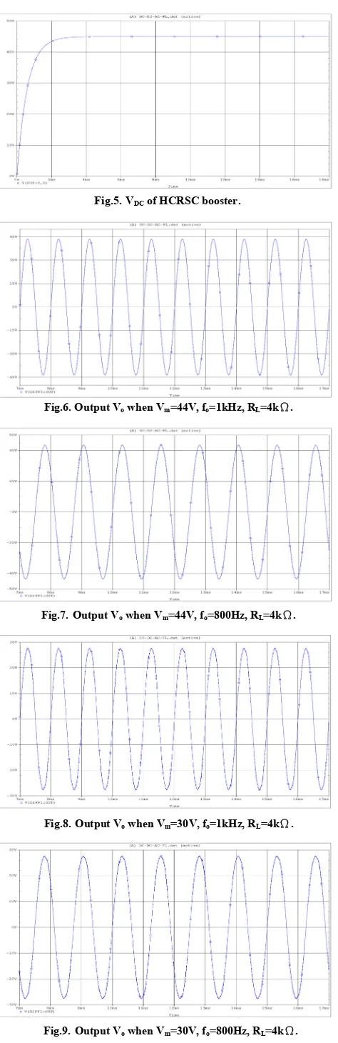
Case I-1: Let the DC-DC booster source Vs be 5V, and then the booster output VDC is about 44.98V (step-up ratio: 3x3) as shown in Fig.5. Now, the sinusoidal peak value and output frequency of Vref are set at Vm=44v, fo=1kHz. And then, as shown in Fig.6, Vo has the peak value of 43.75V, and the practical output frequency is about 1kHz. The efficiency is 76.82%, and THD is 3.9%.
Case I-2: Let the DC-DC booster source Vs be 5V, and then the booster output VDC is about 44.98V (step-up ratio: 3x3) as shown in Fig.5. Now, the sinusoidal peak value and output frequency of Vref are set at Vm=44v, fo=800Hz. And then, as shown in Fig.7, Vo has the peak value of 43.75V, and the practical output frequency is about 800Hz. The efficiency is 78.5%, and THD is 3.1%.
Case II-1: Let the DC-DC booster source Vs be 5V, and then the booster output VDC is about 29.98V (step-up ratio: 3x2). Now, the sinusoidal peak value and output frequency of Vref are set at Vm=28v, fo=1kHz. And then, as shown in Fig.8, Vo has the peak value of 27.8V, and the practical output frequency is about 1kHz. The efficiency is 72.31%, and THD is 2.6%.
Case II-2: Let the booster source Vs be 5V, and then the booster output VDC is about 29.98V (step-up ratio: 3x2). Now, the sinusoidal peak value and output frequency of Vref are set at Vm=28v, fo=800Hz. And then, as shown in Fig.9, Vo has the peak value of 27.8V, and the practical output frequency is about 800Hz. The efficiency is 75.69%, and THD is 2.3%.
B. Dynamic simulation:
Case III-1: Let the source Vs be 5V, and the booster output VDC is 44.98V (step-up ratio: 3x3). we set Vm=39v, fo=1kHz. After the system enters the steady-state, Vs is assumed and changed from 5V to 4.8V as shown in Fig. 10(a). And then, Vo can be obtained as Fig. 10(b).
Case III-2: Let source Vs be 5V, and then the DC-DC booster output VDC is about 29.98V (step-up ratio: 3x2). We set Vm=27v, fo=1kHz. After the system enters the steady-state, Vs is changed from 5V to 4.8V as shown in Fig. 11(a). And then, Vo can be obtained as Fig. 11(b). According to Fig. 10(b) and 11(b), obviously, Vo is still following Vref in spite of source variation.
IV. CONCLUSION
A closed-loop high-conversion-ratio switched- capacitor (HCRSC) boost DC-AC inverter is proposed based on sinusoidal-pulse-width-modulation (SPWM) control to achieve step-up DC-AC inversion and regulation. In this paper we realize a HCRSC boost inverter using SPWM control, and it have the wide range of output voltage and frequency (Vm:4.7V~44V, fo: 500Hz~1.5kHz).
Supply source 5V
Switch capacitor (CA11~CA23)
100uF Load capacitor (CL) 200uF Resistance of capacitor (r) 0.01Ω MOSFET of SC booster
(Cell A1~B2)
Transmission Gate Switch on Resistance 0.01Ω
VDC of Output voltage 4.97V~44.95V Voltage ripple ratio 0.008% Frequency of SC boost 200kHz MOSFET of H-bridge
inverter (SA1~SB2)
MbreakN,MbreakP
MOSFET W/L 20000u/1u,40000u/1u
Diode Dbreak
Inductance of filter 2mH Capacitor of filter 50uF
Output impedance 4kΩ
Output voltage 31.01Vrms
Output frequency 800Hz、1kHz
Fig.6. Output Vo when Vm=44V, fo=1kHz, RL=4kΩ.
Fig.7.Output Vo when Vm=44V, fo=800Hz, RL=4kΩ.
[image:5.595.50.287.45.775.2]Fig.5.VDC of HCRSC booster.
Table I. Components of HCRSC boost inverter.
Fig.8.Output Vo when Vm=30V, fo=1kHz, RL=4kΩ.
[image:5.595.328.554.64.314.2]
By using SPWM control, it is realized that output Vo is following the reference Vref. This compensation is used not only to enhance the regulation to various outputs or source disturbance, but also to increase the difference between the output frequency fo and modulation frequency fpwm so as to make the design of output filter easier for the better THD.
Here, the HCRSC boost DC-AC inverter is simulated by OrCAD, and the results are illustrated to show the efficacy of the proposed scheme. Finally, the circuit is simulated by OrCAD, and then we obtained the results as: the efficiency is about 71.2%-78.2%, and the THD is 2.3%-3.9%. At present, we have implemented the hardware of HCRSC boost DC-AC inverter as show the photo in Fig.12. Next, some more experimental results will be obtained and measured for the verification of our HCRSC boost DC-AC inverter.
REFERENCES
[1] T. Umeno, K. Takahashi, I. Oota, F. Ueno, and T. Inoue, “New switched-capacitor DC-DC converter with low input current ripple and its hybridization,” in Proc. 33rd IEEE Midwest Symposium on Circuits and Systems, Calgary, Canada, pp.1091-1094, 1990.
[2] S. V. Cheong, S. H. Chung, and A. Ioinovici, “Duty-cycle control boosts dc-dc converters,” IEEE Circuits and Devices Mag., vol.9, no.2, pp.36-37, 1993.
[3] O. C. Mak, Y. C. Wong, and A. Ioinovici, “Step-up DC power supply based on a switched-capacitor circuit,” IEEE Trans. on Industrial Electronics, vol.42, no.1, pp.90-97, 1995.
[4] K. D. T. Ngo and R. Webster, “Steady-state analysis and design of a switched-capacitor DC-DC converter,” IEEE Trans. Aerospace and Electronic Systems, vol.30, pp.92-101, 1994.
[5] H. Chung and A. Ioinovici, “Switched-capacitor-based DC-to-DC converter with improved input current waveform,” in Proceedings IEEE Int. Symp. Circuits and Systems, Atlanta, USA, pp.541-544, 1996. [6] Y.-H. Chang, “Design and analysis of power-CMOS-gate-based
switched-capacitor DC-DC converter with step-down and step-up modes,” Int. J. Circuit Theory and Appl., vol.31, pp.483-511, 2003. [7] Y.-H. Chang, “Design and analysis of power-CMOS-gate-Based
Switched-Capacitor Boost DC-AC Inverter,” IEEE Trans. Circuits Syst.-I: Fundamental Theory and Appl., vol.51, pp.1998-2016, 2004.
Fig.11(b).Output Vo when Vm=27V, fo=1kHz, RL=4kΩ.
Fig.10(b).Output Vo when Vm=44V, fo=1kHz, RL=4kΩ.
Fig.10(a).Source voltage Vs : 5V → 4.8V.
Fig.11(a). Source voltage Vs : 5V → 4.8V.
Fig.12. hardware implementation of SPWM-based inverter.