LINEAR AND NONLINEAR OPTICAL PROPERTIES OF
LOW-DIMENSIONAL STRUCTURES ON VICINAL
SILICON (111) SURFACES
A thesis submitted to THE UNIVERSITY OF DUBLIN
for the degree of Doctor in Philosophy
JULIE JACOB
School of Physics University of Dublin
Trinity College Dublin 2
Ireland
i
DECLARATION
This thesis has been submitted to the University of Dublin for examination for the degree of Doctor in Philosophy by the undersigned.
This thesis has not been submitted as an exercise for a degree to any other university.
With the exception of the assistance noted in the acknowledgements, this thesis is entirely my own work.
I agree that the Library of the University of Dublin may lend or copy this thesis upon request.
Julie Jacob October 2007
School of Physics, University of Dublin, Trinity College, Dublin
Abstract
Reflectance anisotropy spectroscopy (RAS) and second harmonic generation (SHG) have been used to probe various low-dimensional (LD) structures grown on vicinal Si(111) surfaces under ultra-high vacuum (UHV) conditions. Reflectance anisotropy spectroscopy (RAS) spectra of single domain Si(111)-5×2-Au, Si(557)-5×1-Au, Si(111)-4×1-In and Si(111)-3×1-Ag structures showed a large minima in the region below 3 eV, which show a systematically higher polarizability perpendicular to the adsorbate chains, for all the structures. The detail, however, varies with the adsorbate, the reconstruction and the offcut. The RAS spectra of Si(111)-5×2-Au showed changes with offcut angle in the 1 to 3 eV region, where Au-induced structures appear. The variation was found consistent with different populations of single- and double-chain gold structures formed in the region of the steps.
iii The Ag nanostructures were then capped with amorphous Si to form a near-IR transparent protecting layer. The samples were stable to exposure to ambient conditions for significant periods. The RAS spectra were compared to model calculations, which support the conclusion that the metallic nanostructures survived the capping, while the (3×1)-Ag areas not covered by the nanostructures are modified by the deposition of Si. In contrast, the quasi-1D structure of Si(111)-4×1-In did not survive the capping by amorphous Si as the optical signature of the (4×1)-In structure was quenched on capping.
Acknowledgements
I would like to express my sincere gratitude to my supervisor, Prof. John McGilp, for providing me with an opportunity to work in the Surface and Interface Physics Lab. He followed my entire thesis work very closely and always provided solutions to many difficult problems. This work would not have been possible without his guidance and encouragement.
My sincere thanks to Prof.(Mrs.) R.C Aiyer for her guidance and encouragement she rendered during my research career as an M.Phil. student.
Many thanks to Dr. Lee Carroll for introducing me to everything about UHV and other experimental equipments required for this thesis work. I am grateful to Dr. Sandhya Chandola for her suggestions with the sample preparation and for the STM work. Many thanks to Dr. Karsten Fleischer for the experimental help and suggestions during critical situations.
Many thanks to Chris Smith for the ellipsometry measurements and for lending me a computer for my thesis write up. I wish to thank Nial McAlinden for the RAS work on Si(557)-Au. Thanks to John Cunniffe for his help while assembling the UHV components.
Many thanks to Nikos, who was always willing to lend a hand during difficult experimental times in the lab.
I wish to thank John Kelly for allowing me to sit in the post-doc office during my write up and for all the administrative help. Many thanks Joe, Mick, Dave, Patrick, Nigel and Ken for their technical help.
Many thanks to those who happened to be my way, for their help in removing/assembling the bake out panel or the sample manipulator!
v My sincere thanks to Sumesh all his help, support, suggestions and encouragement during the difficult times. I wish to thank all my friends Sumesh & Parvathy, Sibu & Reena, Vamsi & Swarna, Venky & Lakshmi, Satheesh & Bhavna, Uttam & Mahua, Manjula, Rajat, Pratheep, Vinod for the nice party time in Dublin.
Many thanks to Georgeachen, Cicychechi and Appu for inviting me to their house and for the nice food I had during my stay in Dublin. I wish to thank my parents, my sisters and brothers-in-law for all their support and encouragement.
Publications
Optical response of Ag-induced reconstructions on vicinal Si(111) S. Chandola, J. Jacob, K. Fleischer, P. Vogt, W. Richter, J. F. McGilp
Physica Status Solidi B 2005, 242:3017-3021
Optical and electronic properties of Ag nanodots on Si(111)
S. Chandola, J. Jacob, K. Fleischer, P. Vogt, W. Richter, J. F. McGilp Journal of Physics: Condensed Matter 2006, 18:6979-6986
Reflectance anisotropy studies of the formation of 5×2-Au structures on Si(111) surfaces with different step formations
J. Jacob, N. McAlinden, K. Fleischer, J. F. McGilp Physica Status Solidi B 2007 (Communicated)
Optical second-harmonic generation studies of Si(111)- 3 3-Ag and Si(111)-3×1-Ag grown on vicinal Si(111)
J. Jacob, A. Gomes Silva, K. Fleischer, J. F. McGilp Physica Status Solidi B 2007 (Communicated)
Using reflectance anisotropy spectroscopy to characterize capped metal nanostructures on silicon,
K. Fleischer, J. Jacob, S. Chandola, N. Esser, J. F. McGilp Physica Status Solidi B 2007 (Communicated)
vii
Table of Acronyms
1D One-dimensional
UHV Ultra-high vacuum
LD Low-dimensional
RAS Reflectance anisotropy spectroscopy SHG Second-harmonic generation
RA Reflectance anisotropy
IR Infra-red
SH Second-harmonic
EM Electromagnetic
ML Monolayer
EUV Extreme ultra violet SK Stranski-Krastanov
VW Volmer-Weber
CDW Charge density wave SDW Spin density wave
DAS Dimer-adatom-stacking fault
THEED Transmission high energy electron diffraction STM Scanning tunneling microscopy
STS Scanning tunneling spectroscopy JDOS Joint density of states
SDA Surface dielectric anisotropy LEED Low energy electron diffraction
RHEED Reflection high energy electron diffraction AES Auger electron spectroscopy
HTEZ High temperature effusion cell SUSI Silicon sublimation source FSW Fused silica window PMT Photomultiplier tube
ARUPS Angle resolved ultra-violet photoelectron spectroscopy EELS Electron energy loss spectroscopy
ARPES Angle resolved photoemission spectroscopy QCO Quartz crystal oscillator
DB Dangling bond
LEEM Low energy electron microscopy PEEM Photoemission electron microscopy IPES Inverse photoemission spectroscopy QSE Quantum size effects
ix
Table of contents
Declaration i
Abstract ii
Acknowledgements iv
Publications vi
Table of Acronyms vii
Table of Contents ix
1.
Introduction
1.1 Overview 1
1.2 Optical characterisation techniques and previous work 3
1.3 Thesis outline 5
2.
Low-dimensional structures and their optical response
2.1 Overview 9
2.2 The Si(111) substrate 9
2.2.1 The Si(111)-7×7-surface 9
2.2.2 Vicinal Si(111) surfaces 12
2.3 Low-dimensional structures 14
2.3.1 Self-organised epitaxial growth 14
2.3.2 Metal-induced reconstructions as templates 15 2.3.3 Nucleation of islands on silicon surfaces 16 2.3.4 Electronic properties of LD structures 17
2.4 Optical properties of LD structures 19
2.4.1 Drude-Lorentz oscillator 21
3.
Phenomenology of RAS and SHG
3.1 Overview 26
3.2 Optical response of materials 26
3.3 Reflectance anisotropy spectroscopy 27
3.3.1 Analysis 27
3.4 Second harmonic generation 30
3.4.1 Nonlinear response 30
4.
Experimental details
4.1 Overview 38
4.2 Sample preparation 38
4.2.1 Substrate cleaning 38
4.2.2 In, Au and Ag evaporation source 41
4.2.3 Si evaporation source 42
4.3 Reflectance anisotropy spectrometer 43
4.3.1 RAS experimental configuration 43
4.3.2 RA signal processing 46
4.4 Second harmonic generation 47
4.4.1 SHG experimental configuration 47
4.4.2 Minimisation of errors 49
5.
RAS of anisotropic structures grown on vicinal Si(111)
5.1 Overview 52
5.2 Si(111)-41-In 52
5.2.1 Sample preparation 55
5.2.2 RAS results 56
5.3 Si(111)-31-Ag 59
5.3.1 Sample preparation 61
5.3.2 RAS results 61
5.4 Si(111)-52-Au 64
5.4.1 Sample preparation 67
5.4.2 RAS results - offcut dependence 68
5.4.3 RAS results - preparation dependence 70
6.
RAS of uncapped and capped metal structures
6.1 Overview 75
6.2 Metal nanostructures 75
6.3 Capped nanostructures 77
6.4 In nanostructures 78
6.4.1 RAS results from In nanostructures 78 6.4.2 RAS results from capping studies of Si(111)-4×1-In 79
6.5 Ag nanostructures 81
6.5.1 RAS and STM results from Ag nanodots 81 on Si(111)-3×1-Ag
xi
6.5.3 Offcut dependence 89
6.5.4 RAS results of Si-capped Ag nanostructures 93 6.5.5 Long term stability of capped Ag nanostructures 96
7.
SHG of Ag induced reconstructions and nanostructures
7.1 Overview 101
7.2 SHG of the Si(111)-In, -Au and -Ag systems – previous studies 101
7.3 SHG results 102
7.3.1 SHG results of Si(111)-7×7 103
7.3.2 SHG results of Si(111)-3×1-Ag and Si(111)- 3 3-Ag 103 7.3.3 SHG results of Ag nanodots and Ag islands 109
8.
Conclusions and outlook
8.1 General review 116
8.2 Outlook 119
Appendix
A Description of RAS components 121
1
Introduction
1.1 Overview
2 single nanowire that connect it to the macroscopic world. Fabricating contacts by conventional lithography introduces surface contamination that influences the electronic structure of the nanowire.
1D electron systems can be synthesized at stepped surfaces by self-assembly of atomic and molecular chains. Surface science techniques have been used recently to produce clean and well-ordered arrays of chains at planar surfaces [1-3]. Locking the chains to a crystalline substrate as a superlattice makes it possible to control their spacing with atomic precision. A wide variety of adsorbate and substrate combinations provides opportunities for systematically tailoring electronic properties, such as the intra-chain and inter-chain coupling, the electron count and the Coulomb interaction.
Regular arrays of monatomic steps can be produced on planar Si(111) single crystal surfaces, with periodicities ranging from 2 to 80 nm, and with very low kink densities, due to the highly directional nature of the Si bonding [1]. Tailored arrays of chains can be produced by self-assembly at such surfaces, where nucleation and growth typically initiates at the step edges. Conventional surface science techniques have been used to show that structures such as Si(111)-5×2-Au, Si(111)-3×1-Ag and Si(111)-4×1-In have 1D chain structures of typical width ~1 nm for the individual chains, where the formation of 1D electronic states are expected [1]. These nanostructures are grown by self-assembly and also characterized under ultra-high vacuum (UHV) conditions. The potential of this approach to growing 1D systems is exemplified by the Si(111)-4×1-In system, where recent high brightness synchrotron angle-resolved photoemission studies, in the region 0 to 5 eV below the Fermi level, have provided the first fascinating evidence that the In chains are 1D conducting wires, with a Peierls gap opening at low temperature on formation of a charge density wave, although the latter point remains controversial [4-9]. Further, these surfaces can be used as a template to obtain arrays of quantum dots or anisotropic metal islands [10-13]. The nanodots arrange regularly in a self assembling manner and hence its size and position are highly controllable.
nonlinear optical techniques. Secondly, capping layers are needed on LD structures to protect them from ambient conditions during study or use outside the growth chamber. The presence of a capping layer poses significant problems for surface scientists who wish to examine these interfaces directly at an atomic level. Electron-based techniques, including scanning probe techniques do not penetrate the capping layers. Photon-based techniques are often still applicable, because capping layers at typically ~1 nm -10 nm thick, is less than the absorption depth for optical radiation. A problem to be overcome is that the interfacial spectroscopic signal is often mixed in with very similar bulk-phase signals that can be several orders of magnitude larger. This may make it impossible to extract the desired interfacial spectroscopic information. The key attribute of linear and nonlinear optical techniques used here is the ability to probe both electronic and crystallographic structure at interfaces, while avoiding interference from bulk phases.
1.2 Optical characterisation techniques and previous work
The optical characterisation techniques used in this work are reflectance anisotropy spectroscopy (RAS) and second harmonic generation (SHG). These state-of-the art epioptic [14] techniques exploit the difference in symmetry between the surface or interface and the centrosymmetric structure of substrates such as silicon (and also capping layers) in order to eliminate the normally dominant bulk response [15]. Optical techniques are particularly sensitive to stepped surfaces and interfaces because the symmetry is further reduced [16]. However, anisotropic reconstructions of isotropic bulk exposed planes complicate symmetry considerations. Under these circumstances, the symmetry of the substrate often dictates that a number of symmetry-related domains are formed. For example, singular Si(111) substrates allow three equivalent one-dimensional structures (chain direction [110], [011] and [101]). Stepped silicon surfaces break the three fold symmetry of the substrate and lead to a single domain if the step edge runs along one of the three equivalent chain directions. Hence, the use of stepped surfaces promotes a dominant domain on the surface that will give rise to a RAS signal, whereas equal domain populations ensure the absence of optical anisotropy, even though each domain is itself anisotropic.
4 creating a macroscopically anisotropic surface which can be monitored by RAS and which grows in intensity while preserving its spectral shape until the restructuring of the surface is complete. Once the maximum RA signal has been observed and the restructuring of the surface is complete, further deposition of Au gives rise to the growth of the ( 3× 3) structure, which is optically isotropic. The RA spectrum decays steadily and eventually reduces to zero when the ( 3× 3) structure is complete. RAS studies of both Si(111)-5×2-Au and Si(111)-4×1-In show a dominant linear polarizability perpendicular to the chain and step edges, between 1.5 and 3 eV [18-21]. This is interpreted in terms of electron confinement perpendicular to step edges. These RAS studies did not provide any evidence of quasi-1D metallicity along the chains, as any optical response associated with metallicity was assumed to be in the lower energy. RAS studies of Si(111)-4×1-In extended to lower energy provided evidence for this [19]. RAS shows an emergence of a positive structure below ~1.4 eV consistent with a dominant in-plane linear polarizability along the chains. By extending the spectral range into the infrared (IR), RAS has been utilised successfully to study anisotropic metal islands and isolated wires with direct observation of conductance anisotropy [22-24]. The observed large optical anisotropy directly reflects the morphological anisotropy, which arises from the presence of perfectly aligned self-assembled nanowires. Metallic conductors have Drude-like intraband contribution to the IR spectral region [25]. The observed large positive IR response with dominant polarizability along the long axes of the islands is in the spectral region where anisotropic Drude-like intraband transitions are expected to make significant contribution to the optical spectrum. The response can be modelled by an anisotropic Drude-type dielectric function with two independent tensor components, x andy, contributing to the RAS signal. This simple model appears promising in relating the measured spectra of metallic nanowires and islands to the conductance anisotropy, thus facilitating contactless measurement of this quantity.
symmetries, at either the fundamental or the SH energy. SHG has provided important information on the electronic structure at surface steps [26]. These electronic states have the reduced symmetry of the surface or interface and, in addition, selection of the fundamental and SH electromagnetic field vectors (polarisation vectors) allows different electronic resonances to be accessed, this additional information coming from exciting the various independent nonlinear susceptibility tensor components [27].
SHG studies of Si(111)-4×1-In show that the SH intensity is a factor of six greater when the electric field vectors are aligned along the In chains, compared with alignment orthogonal to the chains [28].This appears to be the 1D equivalent of the general observation that the nonlinear susceptibility of metals is larger than that of semiconductors or insulators, due to the increased polarizability, in the optical region of the spectrum, of electrons in metallic systems. There have been a number of SHG studies of Ag structures on Si(111), mostly concerned with investigating the origin of oscillations of the SH intensity with film thickness above 1 ML coverage [29-34]. In addition, the sensitivity of SHG to surface symmetry has been used to probe the symmetry of the 3×1 and 3 3
reconstructions on singular Si(111) [35-37].
Self-organised nanostructure arrays are also ideal test structures to investigate changes in metallic properties upon capping. Optical techniques like RAS and SHG are very well suited to probe the properties of buried nanostructures, as their penetration depth is much larger than that of conventional surface probes, and the lower symmetry of aligned nanostructures helps to discriminate the nanostructure response from the residual interface, bulk and capping layer response [16].
1.3 Thesis outline
The main aim of this work is to use the epioptic [14] techniques like RAS and SHG to identify the optical signatures associated with the various low dimensional structures. The outline of thesis chapters is as follows:
6 discussed. Chapter 6 presents and discusses the RAS of island structures formed on anisotropic surface reconstructions on offcut Si(111) surfaces and the RAS of In and Ag nanostructures capped using silicon. Chapter 7 presents SHG measurements of
Si(111)-3
3 -Ag, Si(111)-3×1-Ag, silver nanodots and silver islands. Chapter 8 gives the summary and outlook for future work.
References
1. Himpsel FJ, Altmann KN, Bennewitz R, Crain JN, Kirakosian A, Lin JL, McChesney JL: One-dimensional electronic states at surfaces.Journal of Physics-Condensed Matter 2001, 13:11097-11113.
2. Himpsel FJ, Jung T, Kirakosian A, Lin JL, Petrovykh DY, Rauscher H, Viernow J:
Nanowires by step decoration.MRS Bulletin 1999, 24:20-24.
3. Himpsel FJ, Jung T, Ortega JE: Nanowires on stepped metal surfaces.Surface Review & Letters 1997, 4:371-380.
4. Kumpf C, Bunk O, Zeysing JH, Su Y, Nielsen M, Johnson RL, Feidenhans'l R, Bechgaard K: Low-temperature structure of indium quantum chains on silicon.
Physical Review Letters 2000, 85:4916-4919.
5. Yeom HW, Takeda S, Rotenberg E, Matsuda I, Horikoshi K, Schaefer J, Lee CM, Kevan SD, Ohta T, Nagao T, Hasegawa S: Instability and charge density wave of metallic quantum chains on a silicon surface.Physical Review Letters 1999,
82:4898-4901.
6. Sakamoto K, Ashima H, Han Woong Y, Uchida W: Angle-resolved
high-resolution electron-energy-loss study of In-adsorbed Si(111)-(4*1) and -(8*2) surfaces.Physical Review B-Condensed Matter 2000, 62:9923-9926.
7. Yeom HW, Horikoshi K, Zhang HM, Ono K, Uhrberg RIG: Nature of the broken-symmetry phase of the one-dimensional metallic In/Si(111) surface.Physical Review B (Condensed Matter and Materials Physics) 2002, 65:241307-241301. 8. Tsay SF: Atomic and electronic structure of the (4*1) and (8*2) In/Si(111)
surfaces.Physical Review B (Condensed Matter and Materials Physics) 2005,
71:35207-35201.
9. Gonzalez C, Ortega J, Flores F: Metal-insulator transition in one-dimensional in-chains on Si(111): combination of a soft shear distortion and a double-band Peierls instability.New Journal of Physics 2005, 7.
10. Kuntze J, Mugarza A, Ortega JE: Ag-induced zero- and one-dimensional nanostructures on vicinal Si(111).Applied Physics Letters 2002, 81:2463-2465. 11. Owen JHG, Miki K: Growth of Ag nanoclusters on a 1D template.Surface
Science 2006, 600:2943-2953.
12. Zhachuk RA, Teys SA, Dolbak AE, Olshanetsky BZ: Formation of ordered arrays of Ag nanowires and nanodots on Si(557) surface.Surface Science 2004,
565:37-44.
13. Hirayama H, Horie R, Takayanagi K: Nucleation of Ag nanodots at the Si(111)3*1-Ag surfaces.Surface Science 2001, 482-485:1277-1282.
14. McGilp JF: Optical second-harmonic generation for studying surfaces and interfaces.Journal of Physics Condensed Matter 1989, 1:85-92.
15. McGilp JF: Optical Characterization of Semiconductor Surfaces and Interfaces.Progress in Surface Science 1995, 49:1-106.
16. McGilp JF: Optical response of low-dimensional In nanostructures grown by self-assembly on Si surfaces.Physica Status Solidi a-Applied Research 2001,
17. Power JR, Weightman P, O'Mahony JD: Strong optical anisotropy of the single-domain 5*2-Au reconstruction on vicinal Si(111).Physical Review B-Condensed Matter 1997, 56:3587-3590.
18. Pedreschi F, Omahony JD, Weightman P, Power JR: Evidence of electron confinement in the single-domain (4*1)-In superstructure on vicinal Si(111).
Applied Physics Letters 1998, 73:2152-2154.
19. Fleischer K, Chandola S, Esser N, Richter W, McGilp JF: Reflectance anisotropy spectroscopy of Si(111)-(4*1)-In.physica status solidi (a) 2001, 188:1411-1416. 20. Fleischer K, Chandola S, Esser N, Richter W, McGilp JF: Phonon and polarized reflectance spectra from Si(111)-(4*1)In: evidence for a charge-density-wave driven phase transition.Physical Review B (Condensed Matter and Materials Physics) 2003, 67:235318-235311.
21. Fleischer K, Chandola S, Esser N, Richter W, McGilp JF, Schmidt WG, Wang S, Lu W, Bernholc J: Atomic indium nanowires on Si(111): the (4*1)-(8*2) phase transition studied with reflectance anisotropy spectroscopy.Applied Surface Science 2004, 234:302-306.
22. Jalochowski M, Strozak M, Zdyb R: Reflectance anisotropy during growth of Pb nanowires on well ordered Si(3 3 5) surface.Applied Surface Science 2003,
211:209-215.
23. Strozak M, Hnatyuk V, Jalochowski M: Optical properties of Pb nanowires on Si(3 3 5).Vacuum 2004, 74:241-245.
24. Fleischer K, Chandola S, Herrmann T, Esser N, Richter W, McGilp JF: Free-electron response in reflectance anisotropy spectra.Physical Review B (Condensed Matter and Materials Physics) 2006, 74:195432-195410.
25. Johnson PB, Christy RW: Optical constants of the noble metals.Physical Review B (Solid State) 1972, 6:4370-4379.
26. Power JR, O'Mahony JD, Chandola S, McGilp JF: Resonant Optical 2nd-Harmonic Generation at the Steps of Vicinal Si(001).Physical Review Letters 1995, 75:1138-1141.
27. McGilp JF: Second-harmonic generation at semiconductor and metal surfaces.
Surface Review and Letters 1999, 6:529-558.
28. Chandola S, McGilp JF: Optical second harmonic generation at Si(111)-In interfaces: Evidence of quasi-one-dimensional metallicity.physica status solidi (a) 2001, 184:111-116.
29. Pedersen TG, Pedersen K, Kristensen TB: Optical second-harmonic generation from Ag quantum wells on Si(111)7*7: Experiment and theory.Physical Review B-Condensed Matter 1999, 60:R13997-14000.
30. Pedersen K, Kristensen TB, Pedersen TG, Morgen P, Li Z, Hoffmann SV: Optical second-harmonic generation and photoemission from quantum well states in thin Ag films on Si(1 1 1).Surface Science 2001, 482-485:735-739.
31. Hirayama H, Kawata T, Takayanagi K: Oscillation of the optical second-harmonic generation intensity during Ag thin film growth on a Si(111)7*7 surface.Physical Review B-Condensed Matter 2001, 64:195411-195415. 32. Hirayama H, Komizo T, Kawata T, Takayanagi K: Changes of phase and
intensity of optical SHG with Ag deposition on Si(111)-7*7 surfaces.Applied Surface Science 2002, 190:108-112.
33. Hirayama H, Yamasaki A, Kawata T: Change of optical second harmonic generation intensity during Ag deposition on Si(111)7*7 and
Si(111)sqrt[3]*sqrt[3]-Ag surfaces.Surface Science 2003, 532-535:922-927. 34. Hirayama H, Watai M: Two-photon resonance in optical second harmonic
8 35. Dongmei D, Suzuki T: Nucleation and growth of Si(111)-sqrt[3]*sqrt[3]-Ag
investigated in situ using second-harmonic generation.Physical Review B (Condensed Matter and Materials Physics) 2005, 72:85308-85301.
36. Deng D, Suzuki T: Si(111)-3*1-Ag reconstruction studied in situ at elevated temperatures by second-harmonic generation.Japanese Journal of Applied Physics, Part 2 (Letters) 2004, 43:510-512.
37. Venkataraghavan R, Aono M, Suzuki T: Studies on the nucleation, dynamics and structure of the Si(111)-sqrt[3]*sqrt[3]-Ag surface using surface
2
Low-dimensional structures and their optical response
2.1 Overview
The first section of this chapter introduces the singular Si(111) surface, and the dimer adatom stacking-fault model for its 7×7 reconstruction. A brief outline of vicinal Si(111) surfaces is also given. Low-dimensional nanostructures grown by self-assembly and their electronic and optical properties are reviewed in the following sections.
2.2 The Si(111) substrate
2.2.1 The Si(111)-7×7-surface
10 periodically, these energy levels are broadened to make bands: the valence band and the conduction band, respectively. But on the ideal bulk terminated surface there exist dangling bonds (unpaired hybrid orbitals) which are similar to the hybrid orbitals of isolated atoms, whose energy levels will be located between the bonding and anti-bonding states, or within an energy gap. In fact, the dangling-bond state on a clean Si(111) surface is known to lie around the middle of the band gap . But when foreign atoms come to make bonds with the topmost Si atoms, the dangling-bond state will again split into bonding and anti-bonding states. When, furthermore, the adsorbates induce a surface superstructure to form some orbital overlap between neighbouring sites, the bonding and anti-bonding states will again be broadened and become bands. These are surface-state bands, inherent in the surface superstructure. The bands have their own characters, distinct of the bulk electronic states. Figure 2.1 sets out schematically, the formation of surface state bands [1].
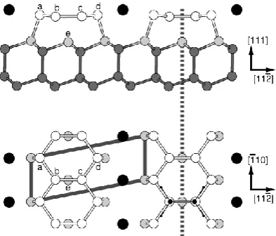
[image:22.595.109.511.335.574.2]The generally accepted structure for the Si(111)-7×7 reconstructed surface is the dimer-adatom-stacking-fault (DAS) model proposed by Takayanagi [2] after scanning tunnelling microscopy (STM) and transmission high-energy-electron diffraction (THEED) studies of the surface. This structure is shown in figure 2.2 [3]. The lozenge of the 7×7-unit cell has corner holes, which are connected to each other by chains of dimers. This unit cell is regarded as containing two triangles separated by the dimer chains. Each triangle has six adatoms (large pink balls) and three rest atoms, arranged locally in a 2×2 periodicity. The
Figure 2.1 A schematic diagram for atoms and molecules, and also the bulk and the surface of a silicon crystal
Electron energy
3p
3s Atomic orbitals
SP3Hybrid
orbitals
Anti-bonding state
Bonding state
Dangling-bond state
Bulk conduction band
Bulk valence band
Surface-state Conduction band
Anti-bonding surface state
Bonding surface state
Surface-state Valence band
Si(111)-7×7 clean surface (sectional views) Dangling bonds Electron energy 3p 3s Atomic orbitals
SP3Hybrid
orbitals
Anti-bonding state
Bonding state
Dangling-bond state
Bulk conduction band
Bulk valence band
Surface-state Conduction band
Anti-bonding surface state
Bonding surface state
Surface-state Valence band
Si(111)-7×7 clean surface (sectional views)
left and right triangles have opposite stacking sequences; the left hand side has a stacking fault (faulted half), while the right does not (unfaulted half). The structure has 19 dangling bonds per 7×7 unit cell, which is a significant reduction in the number of unpaired electrons from 49 at an ideal unreconstructed (111) surface. This leads to a decrease of the total energy, which is, however balanced against an energy increase caused by large angular strains of unusual bondings, such as dimers and adatoms. A review of the models proposed previous to the DAS reconstruction, together with the DAS structure is given by Haneman [4]. Prior to the advent of STM, the 7×7 reconstruction, indicated by electron diffraction techniques, could not be observed on the atomic scale. The first STM topographs obtained by Binning et al. [5] imaged spots within the 7×7 unit cell, at both positive and negative biases, which were thought to be adatoms on an otherwise bulk-terminated substrate. Such a model was shown to lead to high strain, and in any case there was no guarantee that these STM peaks were in fact localized on single atoms. Ion scattering measurements [6-8] could not be explained without the incorporation of a
12 stacking fault into a model for the surface. The lateral sensitivity of THEED work by Takayanagi et al. [2], with calculations of projected atom positions, led to the final structure shown in the figure [3]. This has become the widely accepted model of the Si(111)-7×7 surface.
Data analysis confirmed that the images seen by STM were indeed adatoms and that a fifth layer stacking fault existed in one half of the 7×7 unit cell. STM topographs at different sample biases were made by Tromp et al. [9] and showed a clear asymmetry between opposite halves of the 7×7 unit cell, resulting from the small difference in energy of the dangling bond surface states in the different halves. It has been found by Chou et al. [10] that the stacking fault introduces a surface sate at 0.1 eV above the valence band, dispersing into the valence band. Evidence for the stacking fault and adatoms has also been found in XRD measurements by Robinson et al. [11]. The other major feature of the model is the existence of dimers which delineate the sides of each half of the unit cell.
The effect of the DAS 7×7 reconstruction is to reduce the number of dangling bonds per unit cell. However, the surface is still reactive and possible adsorption sites include direct adsorption onto the dangling bonds, substitution for the adatoms, and adsorption in the corner hole, or breaking of the dimer bonds. All these adsorption sites affect the dangling bonds and any surface states associated with them.
2.2.2 Vicinal Si(111) surfaces
[16], Gd/Si(111) [17] , Au on Si(337), Si(557), Si(5 5 12) [18, 19] or Ag/Si(5 5 12) surfaces.
The Si(111)-7×7 surface has a particularly stable step geometry. The top edge of an equilibrated step consists of a string of corner holes of the 7×7 unit cell, running along the [110] direction [20-22]. Thereby, the 7×7 reconstruction helps ordering the step arrays by quantizing the terrace width in units of half the 7×7 unit cell [23]. This still leaves two possible orientations of the step edge, where the surface normal is tilted from (111) towards opposite directions, i.e., [112] and [112]. Due to the symmetry of bulk Si crystal structure, the surfaces misoriented towards these directions have inherently different structures from each other. Figure 2.3 shows the ideally truncated surfaces of misoriented Si(111) crystal toward [112] (left) and [112] ( right) directions, respectively. These two surfaces have different chemical bond configurations at step edges; only one dangling bond (DB) at a step-edge Si atom for the [112]-directed miscut, while two DBs for the [112] case [24]. The steps with the [112] tilt are taken as the most stable configuration since they are found to occur during Si-on-Si(111) epitaxy [25]. Arrays of single steps can be obtained from samples cut 1.1o towards [112] using a multi-stage annealing sequence [26]. The most critical part is a quench to 850oC within 3 s for avoiding step tripling. Rapid quenching through step bunching regions allows preserving the single-height steps that are stable at high temperature. Thermal disorder from the quench can be removed in a post anneal at lower temperatures, where the mobility is too low for step bunching. However, if
14 this temperature is too high, i.e., too close to the 7×7-to1×1 phase transition at ~870oC, some of the single steps convert to triple steps. Arrays of bunched steps occur for miscut towards [112] direction, with adjustable height (1-5 nm) and a spacing of 70 nm. By taking into account several parameters such as miscut angle, annealing sequence, current direction, external stress; straight edges and regular spacing can be obtained [12, 26].
2.3 Low-dimensional structures
The most commonly used techniques for the preparation of LD nanostructures are lithography, electrochemical deposition and self-organised growth on structured or stepped surfaces. The conventional lithographic methods use UV light from excimer lasers. The structure size is limited by the wavelength of the laser light (currently λ = 193 nm or 157 nm). The node size in commercially available CMOS devices is 45 nm - already below the diffraction limit of λ/2. This can only be achieved by an enormous precision in the manufacturing steps and huge effort in mask design. Other lithographic methods such as electron beam lithography, or the direct scratching of the photoresist using an atomic force or scanning tunnelling microscope can produce much smaller structures, but not in large quantities or on large areas as required for device production. A promising approach to reduce the structure size with conventional lithographic techniques is EUV-lithography (extreme ultraviolet, 13 nm), [27, 28].
Other methods of growing nanostructures have been discussed recently [29, 30]. Metallic nanowires can be grown by electrochemical deposition of metals in structured membranes which are then dissolved in later production steps [29, 31, 32]. The width of wires produced in such a way is determined by the membrane pore size and the length by its thickness. Currently, the only way to produce large areas of organised nanostructures of minimum dimension <5 nm is by self-assembly on structures substrates, particularly stepped surfaces.
2.3.1 Self-organised epitaxial growth
this layer increases. In general, either plastic or elastic relaxation of this internal elastic energy is possible. During plastic relaxation, the elastic energy is reduced by misfit dislocations at the substrate/layer interface; this process competes with elastic relaxation leading to self-organized nanostructures. Elastic energy relief is important for the formation of self-assembled nanostructures, and this in turn depends substantially on layer thickness. For layer thicknesses of only a few MLs, the elastic energy may be reduced by surface reconstruction. The clean surface of a crystalline substrate is often reconstructed in relation to a bulk exposed plane. Heterogeneous adsorption then leads to further reconstruction, producing an adsorbate induced surface superstructure.
2.3.2 Metal-induced reconstructions as templates for LD growth
Surface superstructures induced by metal adsorption on semiconductor surfaces have now become important platforms for exploring LD physics as well as applications to nanotechnology. With various combinations of metal adsorbates and semiconductor substrates an abundance of ordered surface phases has been reported, some of which exhibit intriguing physical properties. Different adsorbates and atomic arrangements form different surface electronic states. Since the surface superstructures generally involve one or two surface atomic layers, their surface state bands are inherently two dimensional. One-dimensional electronic bands may be created due to strongly anisotropic atomic arrangements in surface superstructures. For nano-structural fabrication, usually a thin epilayer is grown on a substrate. This two-dimensional (2D) layer may be used to fabricate lower dimensional structures like wires (1D) or dots (0D) by lithographic techniques. However, structures smaller than the limits of lithographic techniques can only be obtained by assembled growth utilizing the principles of Stranski-Krastanov (SK) or Volmer Weber (VW) growth. Small islands can exhibit unusual quantum confinement effects, which make them useful in electrical devices as single electron transistors and optical devices.
16 reconstruction before adsorption. In some cases it is possible to grow larger anisotropic islands. Examples are the formation of Sn islands on InAs(110) [37] or Pb islands on Si(335) [38], Ag islands on Si(111)-3×1-Ag [33], InGaAs islands on GaAs [39]. In these systems the island size and also shape is determined by the amount of metal deposited. The width, height and length of the island change when more material is deposited. With appropriate growth conditions, self-assembled epitaxial islands can be grown in reasonably well-controlled sizes. A narrow size distribution is essential for most optoelectronic applications. The ability to grow such size-controlled islands is an attractive feature of self-assembly, although the positions of individual islands cannot be determined precisely. Since precise placement of islands is not required for many devices, self-assembly is an attractive route for the fabrication of devices based on nanostructures.
2.3.3 Nucleation of islands on silicon surfaces
Growth of surface structures as described above involves deposition of atoms onto a surface, subsequent diffusion of those adatoms on the surface, and eventually nucleation of adatom clusters, commonly called islands. As atoms are deposited onto a surface they are adsorbed and begin to migrate at non-zero temperatures. Nucleation proceeds as long as adatoms form new islands instead of attracting to the existing ones. A stationary state is reached when the number of islands N remains constant and only island size changes. N scales as a power-law with respect to the surface diffusion coefficient D and the incoming flux F [40, 41] . This implies that the surface diffusion coefficient D can be found by measuring the number of islands on a surface. The scaling relation is given by [40]
x
F
D
N
~
(2.1)where x is the scaling exponent which depends on the spatial dimension d, various microscopic surface processes and the critical island size. For islands on a singular surface, the relevant length scale is determined by the typical distance between islands ln, which is
set during submonolayer deposition. Incoming adatoms nucleate new islands, since in this initial stage of growth there are no steps or islands present where newly landed adatoms could attach. Nucleation terminates when a saturation regime is reached, and all incoming adatoms attach to already existing islands. Consequently, the total number of islands remains constant.
6 / 1 ~ F D
ln (2.2)
where D is the adatom diffusion coefficient and F is the flux. When island growth occurs on terraces of a vicinal surface, the terrace width L appears also as a length scale. On a terrace with smaller L most adatoms attach to the step edge and only a few islands appear [43]. On a vicinal surface in the limit of large terraces, L>>ln , in the submonolayer
regime, the island density N (number of islands per unit area) will scale as on a singular surface, 3 / 1 2 ~ 1 D F l N n (2.3) As the terrace width decreases, adatoms attach preferentially to steps instead of nucleating new islands. If L is small enough (step-dominated nucleation), only one island fits between the edges of neighbouring steps. The nucleation length of the islands on a small terrace is given by [44]
5 ~ ~ L F D
ln (2.4)
and consequently the island density in this regime is given by D FL L l N n 4 ~ ~1 ~ (2.5)
Setting the expressions for the island densities equal, N N~, results for a cross-over value of the flux Fc = D/L6, or the terrace width Lc = (D/F)1/6. During the nucleation period the
distance between the islands decreases until the saturation density is reached. 2.3.4 Electronic properties of LD structures
In LD systems, confinement of the electrons in at least one dimension strongly modifies the properties of the system. Low dimensions amplify the role of quantum fluctuations and enhance correlations. Both the ground state and the excitations exhibit strong correlation effects and possess a number of exotic properties, such as charge density waves (CDWs), Peierls instabilities, or the formation of non-Fermi-liquid-like ground states [45-48].
low-18 lying elementary excitations-a rarefied gas of ‘quasi-particles’. These quasi-particles evolve continuously out of the states of a free Fermi gas when interactions are switched on adiabatically, and are in one-to-one correspondence with the bare particles (adiabatic continuity). They possess the same quantum numbers as the original particles, but their dynamical properties are modified by the interactions. This scenario emerges because the phase space for scattering of particles is severely restricted by Fermi statistics: at low temperatures (T/EF << 1) most particles are frozen inside the Fermi sea, and only a fraction
participate in the scattering processes. The restriction to lowlying excitations, implying low densities of excitations, and Fermi statistics are enough to ensure Fermi Liquid properties. In an ideal 1D system, the only possible scattering requires full momentum transfer. Hence interactions between single electrons will be much larger than in the 2D and 3D case. On the microscopic level, the central problem in the theory of interacting electrons is the Peierls instability. For a strictly 1D metal, a model of the band structure and the Fermi surface is shown in figure 2.4 (left). Assuming the band is crossing the Fermi level at half the Brillouin zone, it can be seen that any periodic distortion with a periodicity of 2 real space unit cells will lead to a backfolding of the band at the new zone boundary. This is always accompanied with an energy gain of electrons at the Fermi surface of ΔEP due to the opening of a gap as depicted in figure 2.4 (right). The argument can be similarly formulated for any kF, though the distortion then involves more than two unit cells. Peierls
and Frohlich discussed these phenomena in terms of the electron-phonon interaction. The periodic lattice distortion of 2kF leads to the energy gain and a periodic modulation of the
charge called a charge density wave (CDW) [49]. This instability of 1D metallic structures against CDWs accompanied with periodic lattice distortions (or vice versa) is now known as Peierls instability. For electrons in 1D, any many-body interaction that causes a 2kF
distortion would lead to a more stable configuration than the metallic band. Repulsive electron-electron interaction would lead to similar effects eg. the Mott transition. Also, a periodic modulation of the spins – a spin density wave (SDW) – would lead to an energetically favoured configuration and an opening of a pseudogap at kF. In addition, the
2.4 Optical properties of LD structures
For bulk semiconductors the most important contribution to the dielectric function in the visible spectral range is interband transitions. The dielectric function of Si is shown in figure 2.5 (left). The maxima in can be attributed to certain transitions within the electronic band structure as shown in the right graph of figure 2.5. The absorption and also Im() are large whenever the joint density of states (JDOS) is maximised. The two features at about 3.5 eV and 4.3 eV are labeled E1 and E2 and are related to aspects of the band structure as shown in the right hand graph of figure 2.5. The band edge absorption is completely negligible compared to the absorption coefficient in the spectral region around E1 and E2. This is a consequence of two factors. Firstly, the band edge absorption is weak because it is indirect, and secondly, the density of states at the band edge is comparatively small. The measured absorption is dominated by direct, k-conserving transitions at photon energies where the density of states is high. The band gap Eg is indirect and has a value of 1.1 eV, with the conduction band minimum located near X-point of the Brillouin zone. Direct transitions can take place between any state in the valence band and the conduction band states vertically above it, if the transitions are dipole allowed. The minimum direct
Figure 2.4 Graphical explanation of the energy gain at the Peierls transition. A system with a parabolic metallic state with kF =1/2(π/a)can gain energy by a distortion of periodicity 2a. The
backfolding of the band leads to a gap opening at 1/2(π/a) with a Peierls gap (∆Ep). Since no
20
separation between the conduction and valence bands occurs near the L point, where the transition energy is 3.4 eV. The energy of these transitions is labelled E1, and corresponds to the sharp increase in the absorption at 3.4 eV, observed in the data shown in figure 2.5 (left). The separation of the conduction and valence bands near the X point is also significant. This energy is labelled E2 and corresponds to absorption maximum at 4.3 eV [52]. The transitions near the L and X points are particularly important because of the ‘camel’s back’ shape of the conduction band, leading to conduction and valence bands being approximately parallel to each other. The joint density of states factor is therefore very high at E1 and E2. The maxima in the JDOS or Im() are usually called critical point energies.
For the discussion of the optical properties of nanowires there are two important points regarding the interband transitions. Firstly, since no free standing nanowires are investigated, the reflectivity of the substrate will the influence optical measurements. Optical models will have to be developed to relate structures in the measured spectra to the wires themselves. Secondly, the interband transitions of the nanowire will differ from the bulk, and will vary with size of the wire. Models are needed in order to relate structures in the optical spectra to the properties of the nanowires
2.4.1 Drude-Lorentz oscillator
The simplest models of absorption and dispersion are due to Lorentz and Drude. The Lorentz model can be applied to direct interband transitions; i.e., all transitions for which the final state of an electron lies in a different band but with no change in k-vector in the reduced zone scheme. The Drude model can be applied to intraband transitions.
Within the the Lorentz model, the dielectric response at frequency ω for an isotropic medium is given by
2 2
2 2 2 0 2 2 2 2 2 2 0 2 2 0 2 4 4 1 m e m Ne (2.6)where and are the real and imaginary part of the dielectric function, N denotes the charge density, m the electron mass,the damping factor, e the electron charge and0 is the oscillator position where absorption is maximum.
The region below the interband transitions can be assumed to be nearly free-electron-like and can be described within the Drude model, which describes the absorption of an electron gas. The Drude model for metals is obtained directly from the Lorentz model by equating the restoring force to zero as the conduction electrons of a metal are assumed not to be bound. Furthermore, because the wavefunction for a free electron is distributed fairly uniformly throughout the metal, the field acting is just the average field. Taking0 0, equation (2.6) becomes
2 2
2 2 2 2 4 1 4 1 m Ne m Ne (2.7)
22 absorption remains valid. The Drude model of non-interacting electrons is a rather crude model. Nevertheless the agreement with the IR response of metals and also doped semiconductors is astonishing if the electron mass is replaced by the effective mass,m*, which accounts for interactions of the electrons with the screened core potentials. In figure 2.6 is shown for several metals [54].
.
Quasi-1D nanowires are structurally anisotropic and are expected to produce an anisotropic optical response. The optical anisotropy is most simply described by anisotropic values of the effective masses and/or scattering rates. The full anisotropic dielectric function,i, can be described by the combination of Drude term and Lorentz oscillators, which account for the intraband absorption of the free electrons and the interband absorptions, respectively:
2 2
2 2 2, 0 1 2 2 2 2 2 2 2 2 , 0 2 2 , 0 1 2 2 2 1 i i i i n j i i p i i i i i n j i p i A A
(2.8)for i=x, y in the surface plane. Here, the amplitudeAiis proportional to the oscillator strength, i is the damping, 2p 4Ne2/m* is the plasma frequency squared and m* is the effective mass. The parameters can be adjusted to give optimal values by least square fitting to the experimental data.
Figure 2.6 Imaginary part of the dielectric function for various metals. For all metals the characteristic Drude tail of the free carrier absorption is observed in the infrared. Additional structures arise from interband transitions [54].
References
1. Hasegawa S: Surface-state bands on silicon as electron systems in reduced dimensions at atomic scales.Journal of Physics Condensed Matter 2000,
12:R463-495.
2. Takayanagi K, Tanishiro Y, Takahashi M, Takahashi S: Structural analysis of Si(111)-7*7 by UHV-transmission electron diffraction and microscopy.Journal of Vacuum Science and Technology A (Vacuum, Surfaces, and Films) 1985,
3:1502-1510.
3. Woodruff DP: Solved and unsolved problems in surface structure determination.Surface Science 2002, 500:147-171.
4. Haneman D: Surfaces of silicon.Reports on Progress in Physics 1987, 50: 1045-1086.
5. Binnig G, Rohrer H, Gerber C, Weibel E: 7*7 reconstruction on Si(111) resolved in real space.Physical Review Letters 1983, 50:120-123.
6. Culbertson RJ, Feldman LC, Silverman PJ: Atomic displacements in the Si(111)-(7*7) surface.Physical Review Letters 1980, 45:2043-2046.
7. Tromp RM, van Loenen EJ, Iwami M, Saris FW: On the structure of the laser irradiated Si(111)-(1*1) surface.Solid State Communications 1982, 44:971-974. 8. Aono M, Souda R, Oshima C, Ishizawa Y: Structure analysis of the Si(111)7*7
surface by low-energy ion scattering.Physical Review Letters 1983, 51:801-804. 9. Tromp RM, Hamers RJ, Demuth JE: Atomic and electronic contributions to
Si(111)-(7*7) scanning-tunneling-microscopy images.Physical Review B (Condensed Matter) 1986, 34:1388-1391.
10. Chou MY, Cohen ML, Louie SG: Theoretical study of stacking faults in silicon.
Physical Review B (Condensed Matter) 1985, 32:7979-7987.
11. Robinson IK, Waskiewicz WK, Fuoss PH, Stark JB, Bennett PA: X-ray diffraction evidence of adatoms in the Si(111)7*7 reconstructed surface.
Physical Review B (Condensed Matter) 1986, 33:7013-7016.
12. Viernow J, Lin A-L, Petrovykh DY, Leibsle FM, Men FK, Himpsel FJ: Regular step arrays on silicon.Applied Physics Letters 1998, 72:948-950.
13. Teichert C: Self-organization of nanostructures in semiconductor heteroepitaxy.Physics Reports 2002, 365:335-432.
14. Gambardella P, Blanc M, Brune H, Kuhnke K, Kern K: One-dimensional metal chains on Pt vicinal surfaces.Physical Review B (Condensed Matter) 2000,
61:2254-2262.
15. Gambardella P, Blanc M, Burgi L, Kuhnke K, Kern K: Co growth on Pt(997): from monatomic chains to monolayer completion.Surface Science 2000,
449:93-103.
16. Yater JE, Shih A, Idzerda YU: Structural characterization of stepped Ga/Si(112) surfaces.Physical Review B: Condensed Matter 1995, 51:7365.
17. McChesney JL, Kirakosian A, Bennewitz R, Crain JN, Lin J-L, Himpsel FJ: Gd disilicide nanowires attached to Si(111) steps.Nanotechnology 2002, 13: 545-557.
18. Himpsel FJ, Altmann KN, Bennewitz R, Crain JN, Kirakosian A, Lin JL, McChesney JL: One-dimensional electronic states at surfaces.Journal of Physics-Condensed Matter 2001, 13:11097-11113.
19. Segovia P, Purdie D, Hengsberger M, Baer Y: Observation of spin and charge collective modes in one-dimensional metallic chains.Nature 1999, 402:504-507. 20. Himpsel FJ, Mo YW, Jung T, Ortega JE, Mankey GJ, Willis RF: Quantum well
24 21. Jung T, Schlittler R, Gimzewski JK, Himpsel FJ: One-dimensional metal
structures at decorated steps.Applied Physics a (Materials Science Processing) 1995, 61:467-474.
22. Phaneuf RJ, Williams ED: Step-height-tripling transition on vicinal Si(111).
Physical Review B (Condensed Matter) 1990, 41:2991-3003.
23. Goldberg JL, Wang XS, Wei J, Bartelt NC, Williams ED: Quantization of terrace widths on vicinal Si(111).Journal of Vacuum Science and Technology A (Vacuum, Surfaces, and Films) 1991, 9:1868-1873.
24. Okino H, Matsuda I, Tanikawa T, Hasegawa S: Formation of facet structures by Au adsorption on vicinal Si(111) surfaces.e-Journal of Surface Science and Nanotechnology 2003, 1.
25. Becker RS, Golovchenko JA, McRae EG, Swartzentruber BS: Tunneling images of atomic steps on the Si(111)7*7 surface.Physical Review Letters 1985,
55:2028-2031.
26. Lin JL, Petrovykh DY, Viernow J, Men FK, Seo DJ, Himpsel FJ: Formation of regular step arrays on Si(111)7*7.Journal of Applied Physics 1998, 84:255-260. 27. Qian T, San-Qiang S, Limin Z: Nanofabrication with atomic force microscopy.
Journal of Nanoscience and Nanotechnology 2004, 4:948-963.
28. Fay B: Advanced optical lithography development, from UV to EUV.
Microelectronic Engineering 2002, 61-62:11-24.
29. Kovtyukhova NI, Mallouk TE: Nanowires as building blocks for self-assembling logic and memory circuits.Chemistry - A European Journal 2002, 8:4354-4363. 30. Murphy CJ, Jana NR: Controlling the aspect ratio of inorganic nanorods and
nanowires.Advanced Materials 2002, 14:80-82.
31. Martin BR, Dermody DJ, Reiss BD, Fang M, Lyon LA, Natan MJ, Mallouk TE:
Orthogonal self-assembly on colloidal gold-platinum nanorods.Advanced Materials 1999, 11:1021-1025.
32. Wirtz M, Martin CR: Template-fabricated gold nanowires and nanotubes.
Advanced Materials 2003, 15:455-458.
33. Hirayama H, Horie R, Takayanagi K: Nucleation of Ag nanodots at the Si(111)3*1-Ag surfaces.Surface Science 2001, 482-485:1277-1282. 34. Kuntze J, Mugarza A, Ortega JE: Ag-induced zero- and one-dimensional
nanostructures on vicinal Si(111).Applied Physics Letters 2002, 81:2463-2465. 35. Ragan R, Kim S, Li X, Williams RS: Platinum passivation of self-assembled
erbium disilicide nanowire arrays on Si(001).Applied Physics A: Materials Science and Processing 2005, 80:1339-1342.
36. Owen JHG, Miki K: One-dimensional epitaxial growth of indium on a self-assembled atomic-scale bismuth template.Nanotechnology 2006, 17:430-433. 37. Fleischer K, Chandola S, Herrmann T, Esser N, Richter W, McGilp JF:
Free-electron response in reflectance anisotropy spectra.Physical Review B (Condensed Matter and Materials Physics) 2006, 74:195432-195410.
38. Strozak M, Hnatyuk V, Jalochowski M: Optical properties of Pb nanowires on Si(3 3 5).Vacuum 2004, 74:241-245.
39. Leonard D, Krishnamurthy M, Reaves CM, Denbaars SP, Petroff PM: Direct formation of quantum-sized dots from uniform coherent islands of InGaAs on GaAs surfaces.Applied Physics Letters 1993, 63:3203.
40. Venables JA, Spiller GDT, Hanbucken M: Nucleation and growth of thin films.
Reports on Progress in Physics 1984, 47:399-459.
42. Pimpinelli A, Villain J: Physics of crystal growth. Cambridge : Cambridge University Press; 1998.
43. Bales GS: Crossover scaling during submonolayer epitaxy on vicinal substrates.Surface Science 1996, 356:439-444.
44. Rusanen M, Koponen IT, Kallunki J: Mixing length scales: Step meandering and island nucleation on vicinal surfaces.European Physical Journal B 2003,
36:141-147.
45. Yeom HW, Takeda S, Rotenberg E, Matsuda I, Horikoshi K, Schaefer J, Lee CM, Kevan SD, Ohta T, Nagao T, Hasegawa S: Instability and charge density wave of metallic quantum chains on a silicon surface.Physical Review Letters 1999,
82:4898-4901.
46. Yeom HW, Horikoshi K, Zhang HM, Ono K, Uhrberg RIG: Nature of the broken-symmetry phase of the one-dimensional metallic In/Si(111) surface.Physical Review B (Condensed Matter and Materials Physics) 2002, 65:241307-241301. 47. Tsay SF: Atomic and electronic structure of the (4*1) and (8*2) In/Si(111)
surfaces.Physical Review B (Condensed Matter and Materials Physics) 2005,
71:35207-35201.
48. Gonzalez C, Ortega J, Flores F: Metal-insulator transition in one-dimensional in-chains on Si(111): combination of a soft shear distortion and a double-band Peierls instability.New Journal of Physics 2005, 7.
49. Peierls RE, Sir, 1907- Quantum theory of solids Oxford : Clarendon University Press 1955.
50. Bardeen J, Cooper LN, Schrieffer JR: Theory of superconductivity.Physical Review 1957, 108:1175-1203.
51. Voit J: One-dimensional Fermi liquids.Reports on Progress in Physics 1995,
58:977-1116.
52. Yu PY, Cardona M: Fundamentals of semiconductors 2. rev. ed.. Physics and materials properties. Springer; 1999.
53. Kittel C: Introduction to solid state physics, 5th edition. Wiley; 1976.
3
Phenomenology of RAS and SHG
3.1 Overview
The first half of this chapter deals with a more detailed discussion of RAS phenomenology. The second half deals with SHG and the phenomenological theories relevant to this work.
3.2 Optical response of materials
The interaction of an EM field of optical frequency, with condensed matter can be described in terms of the polarization amplitude, P(,2,...), induced by the field, E():
P(k,,2,..)0
(1)(k,):E(k,)(2)(k,,2):E2(k,)...
(3.1))
(i
the square of the EM field, describes the lowest order nonlinear optical response responsible for SHG.
3.3 Reflectance anisotropy spectroscopy
Reflection anisotropy spectroscopy (RAS) is a non-destructive optical probe of surfaces capable of operation within a wide range of environments. It achieves its surface sensitivity by a measurement of the difference in reflection of normal incidence plane polarised light in two directions at right angles, from the surface of a cubic crystal. The optical response of bulk signal cancels by symmetry leaving a signal that arises from the lower symmetry of the surface. The surface sensitivity of RAS has been demonstrated on silicon surfaces with observations of surface reconstruction [1, 2], dimer orientations [1, 3], atomic steps [4-6] and strain [7]. The technique has been used to study adsorption on metals [8-11], semiconductor surfaces [12-16] orientation of organic molecules bonded to metal surfaces [17, 18], alkali-induced surface reconstruction [19] and high pressure semiconductor growth [20]. An extensive review of RAS has appeared recently [21].
3.3.1 Analysis
RAS is one of a handful of techniques, including photoluminescence, and spectroscopic ellipsometry, that depend on 1 (equation (3.1)). As mentioned earlier, it measures the difference in the near normal incidence (50) reflectance of linearly polarised light along two orthogonal axes in the surface plane of a crystal.
The geometry of such an arrangement is shown in figure 3.1. Here, Ep refers to light polarised in the plane of incidence, and Es to light polarised perpendicular to the plane of incidence. Reflection from such a surface is described by the well-known Fresnel equations which can be found in [22].
28
j = x, y or z, to be replaced by the single componentb, the isotropic bulk dielectric constant. The division of the sample into three distinct regions, bulk, thin film and vacuum, is known as the three-phase model [23] (figure 3.1).
Using this anisotropic three phase model and the Fresnel equations, expressions may be derived for the s- and p-polarised light from such a surface [23]. As RAS is only concerned with the reflectance of p-polarised light from a p-polarised incident beam, only that equation will be quoted.
sin
cos2 ]sin [ sin cos 1 cos 4 1 0 2 0 2 2 0 2 0 2 0 0 , 0 b zz b b b b b pp
pp i d
r r (3.2) where 2 yy xx
and
2 xx yy 0 pp
r = complex bulk reflection coefficient of p-polarised light from p-polarised incident beam
Figure 3.1 Reflection geometry from a three-phase system, with an exaggerated representation of the angles of incidence and reflection.
![Figure 5.10 (a) LEED pattern of Si(111)-3×1-Ag at 70 eV (b) RA spectra of Si(111)-3×1-Ag on 1o, 2o and 3o offcut towards [ 112] samples, where rrr11](https://thumb-us.123doks.com/thumbv2/123dok_us/1374462.671031/75.595.137.481.69.509/figure-leed-pattern-spectra-si-ag-offcut-samples.webp)
![Figure 5.12 Structural models for gold chain structures on vicinal Si(111). Large circles are Au, small circles are Si, and dark blue circles are Si adatoms (a) Si(557)-Au (b) Si(775)-Au [40]](https://thumb-us.123doks.com/thumbv2/123dok_us/1374462.671031/79.595.126.517.226.438/figure-structural-structures-vicinal-circles-circles-circles-adatoms.webp)