Abstract—Clock jitter and its effects on signal-to-noise ratio
(SNR) were widely investigated in the published literatures. However, most of the issues mainly focused on white-Gaussian-noise-only clock jitter, based on the scenario (assumption) of ideal interference-free clock circuit design which never existed in reality. This paper presents a realistic analog to digital converter (ADC) performance analysis model based on better realistic circuit noise conditions, particularly investigated on the clock jitter error with the combination of Gaussian noise and circuit noise (interference). An analytical expression for the A/D conversion with such combined clock jitter error is developed. The computer simulations are presented, which showed excellent agreement with the developed expression. Also, a real experiment is carried out to bring forth a comprehensive evaluation in A/D system design.
Keywords—analog-to-digital converter, clock jitter,
signal-to-noise ratio, circuit noise
I. INTRODUCTION
The encode source jitter error factor is a key concern in the high speed A/D conversion system design. Walden identified the aperture jitter as the dominating factor that limits the SNR of wideband ADCs[1]. As will be clarified clearly in this paper, clock jitter influences the achievable SNR in a similar way. Lohoning presented an explicit analysis of both the aperture jitter and the clock jitter effects for arbitrary stationary input signals [2]. Bartolome has researched the relationship between clock rising/falling transition time and SNR[3].
However, all of these investigations were based on the assumption of ideal A/D converssion environment, the clock jitter is Gaussian-noise-only. Although it’s highly recommended to avoid this assumption, generally both the white Gaussian noise and the circuit noise (interference) present at the sampling clock simultaneously. Therefore, there is a need to determine the A/D converter output data spectrum when both types of noises present at its input clock. This is the main subject of this paper.
This paper consists of six sections and an appendix. Firstly, The ADC circuit noise and interference model is investigated and a more realistic ADC model with mixture noise. Section III presented an investigation on the mixture noise interfered clock
All authors are with the Dept of Electronic Engineering, School of Information Science & Technology, Beijing Institute of Technology, Beijing, China, 100081
E-mail: {sunlei,an,wyb1982}@bit.edu.cn
error and its effects on A/D SNR and SFDR. Section IV presented a simulation on mixed clock error effects on A/D performance with different error distributions. Section V presented experimental results to illustrate the circuit noise effect on A/D performance, showing that this model is more realistic on A/D analysis than others published. The appendix contains some of the derivations used in this paper.
II. CIRCUIT NOISE AND CLOCK ERROR
Aperture jitter stands for the random sampling time variations in ADCs which are caused by broadband noise in the sample-and-hold circuit. It is commonly modeled as a stationary white Gaussian process[1][2], i.e. the corresponding sampling time variations are assumed to be independent identically distributed (i.i.d.) Gaussian random variables with zero mean value.
Clock jitter is a property of the clock generator that feeds the ADC with the clock signal. It is caused by the phase noise of the oscillator and generates additional sampling time errors in the ADC. Demir declared that the phase noise of free running oscillators can be modeled as a Wiener process [4], i.e., a continuous-time nonstationary random process with independent Gaussian increments. Time-discretization of the Wiener process yields the model of accumulated timing-jitter commonly used for the clock jitter [5] [6], where the sampling time variations are modeled as zero mean value and variance independent.
NGAUSS
ADC
+
Signal input
Digital output
Input noise
+ X
NCROSSTALK
CLOCK
Potential crosstalk current
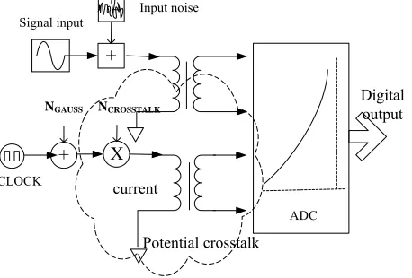
Figure 1. A/D model with circuit noise
The clock error model with Gauss distribution implied the scenario of ideal A/D circuit, while the real system is not always the same. In an actual A/D circuit, the clock circuit is
Circuit Noise Interference on Sampling Clock
and Its Effect on A/D Conversion
[image:1.595.319.548.534.689.2]unable to run independently, without any interference from other circuit noise. It’s always affected by other on-board circuit, and this affection can more or less cause the uncertainty of the sampling clock cycle-to-cycle time, which can also be considered as clock jitter if the affection is tiny.
This paper primarily focuses on the clock error and its effects on A/D performance, only one input sinusoid with white Gaussian noise(Fig.1) is considered. For the clock error, this model consists only one additive white Gaussian noise (NGauss) and a single colored circuit noise (Ncrosstalk ). The approach allows extension to multiple noises in clock error.
Different A/D implementations render different circuit electrical and magnetic noises. Virtually every system includes at least the following noises[7]: power noise, signal cross talking and ground bounce noise. The power noise is caused by the dynamic system current which in return could feed back into the signal routines (paths) and generate noise. The signal crosstalk, which is also called signal serial interference which is mainly caused by the electrical magnetic coupling with parallel wiring. This interference is related to the driver signal frequency and amplitude. The higher signal frequency the higher signal transition speed, resulting in greater coupling amplitude. It is a colored noise. The ground bounce noise is caused by the circuit return current passing through the non-zero ground plane. Due to the complexity of interferences, it’s difficult to characterize all the circuit noise in an uniform mathematical analytical formulation. But generally it can be characterized by an expression including interference frequency and amplitude components [7].
current Victim line Electrical-Magnetic current Driver line Electrical-Magnetic Switching power supply Victim line
Magnetic field
[image:2.595.317.517.368.498.2]ΔT ΔV reference point (b) (a) (c) (d) interferenced point
Figure 2. Circuit noise and clock error
Fig.2-(a) shows a driver signal interfering the adjacent signal (victim line) and resulting in the voltage ripple in Fig 2.-(c). If the interference ripple occurs during the clock rising/falling transition time, the jitter error took place with the interference, in Fig.2-(d).
III. CLOCK JITTER AND ADC PERFORMANCE
The clock jitter with white Gaussian distribution is a
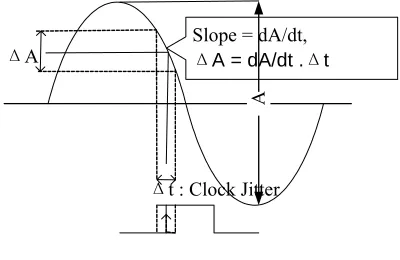
fundamental model and is widely discussed [1-3]. Fig.3 shows that the input signal is a sinusoid with amplitude A and frequency fin. The encode source clock is jitter ∆t, any error in this instant (∆t) will translate an error in voltage (∆A) dependent on the input signal slope.
The total uncertainty in A/D conversion is the sum of all the uncertainties at each point of the sinusoid weighted by the probability of sampling each point [3]:
2 2 0 2 0 2 2 1 ( ( ( )) )
[ sin(2 )] 1
)
1
[ 2 ] 2
T jitter
T in
in
slope A t d T
d A f
t d
T d
A f t
σ τ τ
π τ τ
τ π = ×∆ ⎡ ⎤ = ⎢ ×∆ ⎥ ⎣ ⎦ = ⋅∆
∫
∫
(1)The theoretical limitation of the SNR due to this clock jitter is given by,
2 10 10 2 2 2 1 S 2
SNR = 10log 20log 2
1[ 2 ] 2 in jitter in A f t A f t
π σ π ⎡ ⎤ ⎢ ⎥ = ⎢ ⎥= − ⋅∆ ⎢ ⋅∆ ⎥ ⎣ ⎦ (2)
The ∆t in (2) presents the standard derivation jitter time. The expression (2) states that the SNR is only limited by the signal amplitude, frequency and the clock jitter error.
Slope = dA/dt,
ΔA = dA/dt .Δt
ΔA
Δt : Clock Jitter
A
Figure 3. Clock jitter on sampling uncertainty
As discussed in section II, generally both the white Gaussian noise and the colored circuit noise are present at the sampling clock simultaneously. The A/D conversion analytical expression with the combination clock error of Gauss distribution noise and circuit noise are appended in this paper in which the expression is derived.
0
(
)
sin[ (
)]
(
( , )
i s ss Gauss Crosstalk
n
jk nT j nT
G Gauss k
n k
x nT
A
nTs
t
t
h
t
h
v e
ωe
ωω
ω
+∝ =−∝ +∝ ∝ =−∝ ==
⋅
+ ∆
+ ∆
=
∆
∑
∑ ∑
)
(3)In (3), Ts is the ideal clock cycle, ∆tGauss is Gaussian noise
clock jitter component and ∆tCrosstalk is interfered clock error
component, ω and A are the input signal’s radian frequency and amplitude respectively. ωi and ν present the interference driver
signal’s frequency and amplitude.
[image:2.595.69.266.434.623.2]comprising infinite driver signal’s harmonic components (kωi)
with amplitude hk (ωi,ν) .
IV. SIMULATIONS
In order to verify the above model, series of simulations are presented.
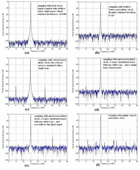
Fig.4 shows the A/D conversion data power spectrum simulated for a input sinusoid with frequency 14.99MHz, the input signal-to-noise ratio is 100dBc with white Gaussian noise. The converter clock frequency is 80MHz.
Figure 4. A/D conversion simulations
Fig.4-(a) presents the conversion power spectrum of ideal clock cycles. Fig.4 -(b) presents a result on clock jitter with an additive white Gaussian noise of standard derivation 2ps. Compared with (a), It’s clear that the added clock jitter raised the noise floor in (b), in another word, decreased the SNR.
Fig.4 -(c) shows the simulation results of signal crosstalk effects on ADC performance. Interference driver signal is a 70MHz sinusoidal noise. Suppose the ADC input clock slope is 1V/ns(typical)[3] , and the interfered clock coupling amplitude is 1mv, which result in the maximum clock error offset with 1ps(∆t=∆v/slope). This colored clock error result in the spur components at frequency bin 5MHz and 25MHz on the power spectrum figure, the amplitude is approximately -85dBc. This simulation shows that a tiny colored noise in clock error, can result in an un-negligible spur component. Fig.4-(d) is the result on clock error with the combination of white Gaussian noise and colored circuit noise. It’s obvious that the floor noise raised with the spur distortion occurred on the power spectrum figure.
Fig.4-(e) presents the simulation of the crosstalk between the
input signal and the sampling clock. Compare to Fig.4-(a), It is found that the harmonic components rise at the 2nd and 3rd signal frequency bin. Fig.4-(f) shows the result of clock error with several independent colored circuit noises.
[image:3.595.57.281.213.485.2]Fig.5 shows colored circuit noise effects on A/D conversion data spur distortion. (a) is to describe the relationship between the input signal frequency and spur distortions. The spur distortion rise from -105dBc to -80 dBc with the input signal frequency changed from 2MHz to 32MHz approximately. Fig.5 -(c)(d) describe the relationship between clock error caused by signal cross-talking into the clock section and the effect on harmonic distortion.
Figure 5. clock error and A/D conversion performance
V. EXPERIMENTS AND ANALYSIS
Fig.4 -(e) brings out more realistic meanings but it is always deceptive to an ADC designers. In a real ADC system, a lot of possibilities can result in harmonic distortion in the A/D conversion. For example, the imperfect suppression of the anti-aliasing filter’s stopband before the ADCs, the non-linearity of the A/D conversion process, or both, could produce unwanted harmonics in the conversion. Those possibilities might mislead the designer to ignore the interference from the on board circuit noises, especially the conversion output digital data which could produce the input signal frequency correlated noise[8] and feed back into the clock circuit by power noise and ground plane coupling, or signal crosstalk. Thus, this sort of clock error is closely-correlated to with the input sampled signal’s frequency which can result in the harmonic distortions in the conversion, i.e., greatly upsetting the spur-free dynamic range (SFDR) performance of an ADC.
[image:3.595.316.533.234.403.2]-90dB, and the SFDR is 78dBc, denote that it’s nearly in ideal working state.
Nowadays, most ADC circuit is designed in such a way that the single-ended signal is coupled into differential form by transformers, in order to reduce the circuit common-mode interference. In order to prove the conceivable possibility of signal-clock crosstalking, we just put the signal transformer lie adjacent to the clock transformer, and remaining the other conditions unchanged. The result under this condition is Fig.6 -(b). Compare with Fig.6-(a), the 2nd harmonic of the signal is raised up from -95dBc to -78dBc. It is believed that the electrical magnetic interference is coupled from the adjacent two transformers, the interference produced clock error results in changes of harmonic amplitude. This experiment is not particular, on the contrary, it can be found in other ADC designs.
Figure 6. Real A/D experiment
Compare the Fig.4-(f) and Fig.6-(a), shows the simulation result in Fig.4-(f) which is very close to the real A/D running result. This implies that the derived analysis results are very close to the real A/D situations.
VI. CONCLUSION
This paper has investigated the clock error characteristics under circuit noise environment and its influences on ADC performance. The investigation reveals that the circuit noise contains more colored noise than white noise. And thus the clock jitter error consists of both white Gaussian noise and colored circuit noise. An analytical A/D conversion expression with combined clock jitter error is developed. This expression shows that the combined clock error can generate infinite harmonic components in converted digital signal. The computer simulations show excellent agreement with the developed expression. Also, a real experiment shown the evidence of the circuit noise influence on A/D performance and brings forth a comprehensive evaluation of analog-to-digital system design. This paper might offer A/D designers a rule of thumb to reduce the discrepancy between the actual circuit performance and the official figures imprinted on data sheet.
APPENDIX
This appendix is the A/D conversion expression with mixed clock error, result of composite effects of white Gaussian noise as well as colored circuit noise.
Scenarios are,
input signal is a sinusoid:
)= )
t t
π in ω
x(t) = Asin(2 f Asin( (A1)
interference driver signal: ∆N f Vi= ( , )ωi (A2) where V is amplitude and ωi is frequency of interference
driver signal. And the A/D conversions with interfered clock error is,
[
]
(jitter) sin ( Gauss Crosstalk) n
x t A ω nTs t t
+∝
=−∝
=
∑
⋅ + ∆ + ∆ (A3)Where,
sin
sin( ) cos[ ( )] cos( ) sin[ ( )]
sin[ ( )]
sin( ) cos( ) cos( )sin( )
s Gauss Crosstalk s Gauss Crosstalk
s total
s total s total
A
A nT t t A nT t t
A nT t
A nT t A nT t
ω ω ω ω
ω
ω ω ω ω
∆ + ∆ + ∆ + ∆
⋅ + ∆
∆ + ∆
=
=
=
( ) cos ) sin( ) sin )
cos( ) sin ) cos( ) cos )
s Gauss Crosstalk s Gauss Crosstalk
s Gauss Crosstalk s Gauss Crosstalk
nT t t A nT t t
A nT t t A nT t t
ω ω ω ω ω ω
ω ω ω ω ω ω
∆ ∆ ∆ ∆
+ ∆ ∆ + ∆ ∆
( )cos( - ( )sin(
( )cos( ( )sin(
(A4)
The ∆tGauss in (4) is a Gaussian random variable and contribute to Gaussian error in conversion. Because the signal crosstalk can be modeled as [5]:
2
2 2
( , )
( , )
ii
K V
H
g V
H
D
ω
ω
+
i
=
(A5)Where K is a function related on driver signal’s amplitude and frequency. It’s a reasonable consumption,
( , )
isin(
i)
0
1
) cos[ sin( )] J J ( )cos(2 )
Crosstalk i i
k
t v t v v k t
ω ω ω ω ∝ ω ω
=
∆ =
∑
2kcos( = ( )+2 (A7)
0
)=sin[ sin( )] J ( )sin( 2 1 )
Crosstalk i i
k
t v t v k t
ω ω ω ∝ ω ω
=
∆
∑
2k+1 ⋅sin( =2 ( +) (A8)
2 0
0
(
/ 2)
J
!(
)!
j k
j
v
v
j k
j
ω
ω
∝ +=
+
∑
(-1)
j(
)=
(A9)where In (9), Jk(ω,ν) is a k-order first class Bessel function. From (7-9), It’s clear that the ∆tcrosstalk component generate infinite harmonic components in the conversion data. By reasonable substitution, the expression (4) can be re-write as,
0
(
)
sin[ (
)]
(
( , )
i s ss Gauss Crosstalk
n
jk nT j nT
G Gauss k
n k
x nT
A
nTs
t
t
h
t
h
v e
ωe
ωω
ω
+∝
=−∝ +∝ ∝
=−∝ =
=
⋅
+ ∆
+ ∆
=
∆
∑
∑ ∑
)
(A10)
(10) is the A/D conversion analytical expression with the combination clock error of Gauss distribution noise and circuit noise.
In (10), Ts is the ideal clock cycle, ∆tGauss is Gaussian noise clock jitter component and ∆tCrosstalk is interfered clock error component, ω and A are the input signal’s radian frequency and amplitude respectively. ωi and ν present the interference driver signal’s frequency and amplitude respectively.
REFERENCES
[1] RH Walden, “Analog-to-digital converter survey and analysis” , IEEE Journal on Selected Areas in Communications, Volume 17, Issue 4, April 1999, pp. 539–549
[2] Lohning M, Fettweis G, The effects of aperture jitter and clock jitter in wideband ADCs , Computer Standards & Interfaces, Volume 29, Issue 1, January 2007, 11-18
[3] Bartolome E, Mishra V, Dutta G, et al., Clocking high speed data converters. http://www.ti.com, TI corp, 2002.
[4] Demir A., Mehrotra A., Roychowdhury J., Phase noise in oscillators A unifying theory and numerical methods for characterization , IEEE Transactions on Circuits and Systems-I: Fundamental Theory and Applications, May 2000, 655–674.
[5] S.S. Awad, Analysis of accumulated timing-jitter in the time domain , IEEE Transactions on Instrumentation and Measurement Feb 1998, 69–73.
[6] Cherry J.A., Snelgrove W.M., Clock jitter and quantizer metastability in continuous-time delta-sigma modulators , IEEE Transactions on Circuit and Systems-II: Analog and Digital Signal Processing , June 1999,661– 676.
[7] P.Vizmuller, RF Design Guide: Systems, Circuits and Equations. Norwood, MA: Artech House, 1995.
[8] Fan Changxin, Communication Theory (in Chinese character), Guofang industry Press, Beijing, 1995, pp.68-71