INTERNATIONAL PROJECT “DIRECTIONAL EDUCATION” FOR SKILLS DEVELOPMENT AND PROFESSIONAL ORIENTATION OF YOUTH IN
NANOTECHNOLOGY
Anzhela V. Andreeva1, Kseniia K.Kuzmina1, Victor V.Luchinin1, Maxim Ya.Pratusevich2 1
Saint Petersburg Electrotechnical University "LETI", Professora Popova Str., 5, 197376 St. Petersburg, Russian Federation
2
Saint Petersburg Physical-Mathematics Lyceum № 239, Kirochnaya Str., 8, 191028 St. Petersburg, Russian Federation
Abstract
Development of Russia is focused on the restoration of basic science, forming national innovation system integrated into the world. It determines the need for increasing the number of scientific and engineering personnel with a high level of competence, creating conditions for creative youth to acquire knowledge and skills for use of its capabilities in high-tech industries. Purpose of the article is a system providing of information on the complex of low-budget education and research laboratories for formation of technologic culture in the field of nanotechnology. The use of these laboratories will take place at three levels: basic, creative and professionally oriented.
Key words: basic, creative and professionally oriented levels, low-budget education and research laboratories, nanotechnology
1. INTRODUCTION
Need to realize the potential of creative youth determines the demand for a modern infrastructure, methodology and staff. Taking into the account that nanotech is based on interdisciplinary knowledge and intersectoral work, and it is the basis of new technological order, the experimental basis for development of laboratory skills and professional orientation of Russian youth become particularly important.
2. REALIZATION OF CREATIVE ABILITIES OF STUDENTS
A set of measures to develop creative abilities of Russian schoolboys which attention is paid to the laboratory and methodological support in new areas of technology and biotechno-sphere in LETI is developed. The complex of nano-laboratories with creatively and professionally-oriented levels is organized. Experimental and methodological support of these laboratories integrated in developing an educational program provides:
• Familiarize students with the possibilities of modern science and technology, • Intensification research activity of schoolboys in the natural sciences, • Support of professional orientation of schoolboys,
• Creation of a positive image of engineers and scientists for schoolboys, • Tightening the links between the school, scientific and university community, • Attracting of new teachers to develop creative potential ofschoolboys,
• Positioning of the school as a center of technological culture– the basis for educational initiatives in science and professionally-oriented education.
The educational program includes: • the list of labs and workshops, • detailed instructions,
• laboratory equipment and software specifications, • laboratory and practical exercise specifications,
• criteria for evaluation of laboratory and practical work, as well as samples of report forms, • guidance for teachers of natural sciences to introduce the proposed works in the training program, • guidance on the organization of the training project, including the technologies, used in the
implementation of educational programs.
The "Nanolaboratory" program has a block-modular adapted to the level of schoolboys’ knowledge, motivation, time resource. It is targeted to schools with in-depth teaching of natural sciences with specialized classes and centers of young creation. Based on the continuity of the educational program, it can be harmonized with the training on nanotechnology in universities in the training areas: nanomaterials, nanotechnology and microsystem technique, electronics and nanoelectronics, nanoengineering.
An educational effect during implementation of the program in addition to an earlier start of schoolboys’ creativeness is determined by: fundamental nature of knowledge, interdisciplinary nature of knowledge, convergence of physical and information components of education, professional orientation of education for skills in the chosen field.
The teachers of natural sciences in the framework of the program will improve skills in the subject areas, carry out the design of specific programs, avoiding imposition of them as addition, workload for schoolboys, and to serve for a better perception of the subject, build the educational process jointly with the teachers of different disciplines.
The innovative nature of the program will contribute to the activity of schoolboys and teachers in the class-lesson system and outside of it. This program can be implemented as part of primary and secondary education programs, facilitated by its modular nature.
Under the proposed program schoolboys will choose the path of its development, including realizing projects, composition of the participants, their role in the projects, plan activities for the implementation of projects, obtain the necessary knowledge, process the results, including their assessment and creating report.
The program provides monitoring of its performance on a number of targets, including amount of schoolboys participating in the "optional" projects voluntarily, number of schoolboys participating in competitions and conferences in science and engineering fields, as well as number of graduates of schools admitted to universities in areas directly related to the nanotechnology.
3. INSTRUMENTATION-TOOL PLATFORM
As earlier noted, the instrument-tool platform involves three levels of equipment for nanolaboratory. The basic level of laboratory, launched LETI in physics and mathematics school № 239, provides basic education in the basic properties of nanomaterials, including the study of heat and electrical conductivity, dielectric permittivity and magnetic permeability. To do this, by the grant of St.-Petersburg Government, the laboratory tables of Finnish company TEKLAB (LETI partner) have been integrated with laboratory equipment of German company PHYWE System. There were made multi-functional computerized displays as the result.
The computerized laboratory stands (Fig.1a) controlled from a workplace instructor (4 pcs.) contain a set of experimental devices and system of access to the computer network and Internet. Installation for production of carbon nanotubes (CNTs) from gas phase
There is an environmentally safe, non-toxic and low-cost synthesis of arrays of vertically aligned CNTs in the reactor and on the surface of the substrate of chemical vapor deposition of the catalytic pyrolysis liquid (S8H10, S6N14, C2H5OH) and gaseous hydrocarbons (C2H2, CH4). The equipment allows to work with volatile (metallocenes, metallophthalocyanines) and localized on the substrate catalyst (Ni, Co, Fe). It is designed for a wide range of education, scientific and research applications
Installation for production of organic nanolayers by Langmuir-Blodgett method
There is a formation of thin films, ability to study these samples, application of nano- and biotechnology, molecular engineering
Installation of molecular chemical assembly
There is a super-precision without nucleation molecular causing oxides and other compounds of aluminum, silicon and heavy metals (hafnium, zirconium) on substrates of semiconductor, metal and dielectric materials
Installation for sol-gel production of structured oxides
There is a formation of thin glass films by spin of the film-forming sols (spin-jn-glass film) with heat treatment
Installation of DNA amplification by polymerase chain reaction
There is an identification of DNA fragments by increasing concentration of the desired fragments amplification followed by detection of them with probes carrying of flyuoroform
Installation of electrochemical formation of nanoporous silicon
There is a formation of nanoporous silicon layers of controlled thickness, porosity (nano-, micro-mesoporous layers) and lateral uniformity on areas up to 20 cm2
Miniature scanning electron microscope The investigation of the surface morphology with micro- and nanometer resolution
Installation of optical microscopy with electrical nanoprobe system
Optic and electric testing of devices of nano- and microsystems techniques on stages of its production as well as finished crystal chips
Compact installation of the electronic vapor-magnetic resonance
Research in the field of solid state physics and physics of condensed materials, chemical, biological objects
(including nanoclusters) in a wide range of temperature (biomedicine, materials science)
Small-sized atomic force microscope for school
Morphologic and topologic analysis with atomic resolution of the micro- and nanoscale objects of inorganic and organic nature and surfaces: construction of planar and 3D– morphology of objects; super-local control of electric potential, distribution of doping levels of the material
Compact ellipsometer The local definition of thickness, of refractive index and roughness of layers on the surface of heterogeneous micro-and nanoelectronic objects
Installation of capillary electrophoresis Investigation of the fractional composition and electrophoretic mobility of nanoparticles
Table 1. Education and research laboratory Nanotechnology and nanodiagnostic.
a) b)
Fig.1. Nanolaboratory in school № 239 for basic science education: a) computerized laboratory bench to study the electrical properties of nanomaterials, b) atomic force microscope to study the
objects of organic and inorganic nature
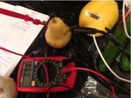
The techniques and programs for implementation and laboratory work have been developed. Training of teachers of the Lyceum by program of excellence in nanotechnology and nanodiagnostics has been completed. Firm NT-MDT to study structural and morphological nanoscale objects to Lyceum the serially produced atomic force microscope Solver NEXT (Fig. 1b) has provided. It allowed to study objects of organic and inorganic nature with the possibility of physical, chemical and biological experiments.
Forming creative-oriented laboratory level will provide a solution to interdisciplinary issues. Composition of nanolaboratory of this level focuses on a different instrumental platform to perform atomic force microscopy facilities and implement a number of technological operations using inorganic and bio-organic materials, including nanolithography, nanocluster and molecular assembly. Actually educational cycle includes laboratory work in physics, chemistry and biology, such as studying of the structure of biopolymers, creating nanoscale gratings, formation of molecular electronic circuits, creation of biodetectors of array-based DNA.
The third level provides of professionally-oriented complex of Nanolaboratory, developed in SEC Nanotechnology of St.- Petersburg SETU (Fig. 2). It takes more than three years of testing and modification (Luchinin V. V., Afanas’ev A. V. 2010). It includes two sectors, implementing research and manufacture of high-tech products on nanoscale (Table 1).
Fig.2. Professionally-oriented scientific and educational complex Nanotechnology and diagnostics
Distinctive features of professionally oriented laboratory are the possibility of using it in education process and in research with formation of knowledge skills, research and small-scale production of hi-tech products. This is to ensure the formation of schoolboys’ competencies for complex scientific and practical activities.
4. PRACTICAL REALIZATION
The program has practical realization in the international project “Directional Education” between Saint-Petersburg Electrotechnical University “LEТI”, Presidential Physics and Mathematics Lyceum № 239 and Portledge School. The principle is to provide a scientific field at different levels of complexity and teaching students according to these levels.
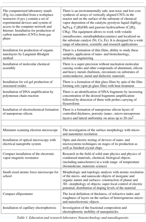
For example, specific guidelines (Andreeva A. V. & Kuzmina K. A. 2014) were written under the project. It explains how to do a research work in the field of nanotechnology without special equipment on the example of two works executed by schoolboys of the fifth and seventh grade. In the first paper the schoolboy made a battery from various fruits and vegetables. He measured EMF of vegetation (Fig. 3). All fruits and vegetables had different EMF. According to the results of the work he conjectured that the EMF of different fluids will also be different and it will be possible to create a prototype of nano tongue that will distinguish tastes of different liquids.
Fig. 3. Measuring EMF of diffrenet vegetation
In the second paper the schoolboy investigated different ways to manage movemen of cockroach (Fig. 4). According to the results of his experiment he found that the best way to manage is to control insects by means of smells.
Fig. 4. Investigation of insect control
Also, a lecture notes for the schoolboys (Luchinin, VV, Andreeva, AV, Baulin, YV, Kuzmina, KA & Lutetskiy, NA 2014) were written under the project. Additionally, author’s educational programs of supplementary education for 5-6, 7-8 and 9-11 years of secondary school and author courses for undergraduate and graduate students ETU LETI were developed. The authors are employees of scientific-educational center "Nanotech" as well as members of the department of micro-and nanoelectronics of ETU LETI.
This program was attended by 18 top lyceum of St. Petersburg, in addition to physical-mathematical lyceum as well as Nakhimov Naval School (Fig. 5).
Fig.5. Schoolboys and students of Nakhimov Naval School are introduced to the school laboratory.
Moreover, a joint pilot project – professional oriented college course "Bionics. Nano cyborgs" are launched in 2014. It is running in the format MOOC (massive open online course). Access - free and open (Lektorium, 2014). This course is an opportunity to acquire knowledge in one of the most sought after and paid areas of modern science. Upon completion of this course, students will become familiar with the features of teaching in a particular university, they will become familiar with modern technologies, equipment and scientific trends, bachelors will get knowledge required in choosing research direction in the Master's degree program and postgraduate training program.
5. CONCLUSIONS
In general, it is important to emphasize that the research and developments in nanosphere prefigure the emergence of motivational factors for the influx of creative young people in the industry. This is a sector of the economy, defining the innovative development of Russia and its entry into the new technological order (Andreeva, AV, Ivanov, AS, Kutuzov, VM, Luchinin, VV & Pratusevich, MYa 2013).
REFERENCES
Andreeva, AV & Kuzmina, KA 2014, Methodological guidance on the implementation and execution of research work in the field of nanotechnology at home (without special equipment), backlist book.
Andreeva, AV, Ivanov, AS, Kutuzov, VM, Luchinin, VV & Pratusevich, MYa 2013, ‘Development in nanotechnology of skills and professional orientation of youth’, NANOINDUSTRY, vol. 1, pp. 60-65. Lektorium, 2014, MOOC-course “Bionics. Nano cyborgs”, http://www.lektorium.tv/mooc/bionika-nano-kiborgi.
Luchinin, VV, Andreeva, AV, Baulin, YV, Kuzmina, KA & Lutetskiy, NA 2014, Research workshop in the field of nanotechnology and nanoelectronics, backlist book.
Luchinin, VV & Afanas’ev, AV 2010, ‘The Study-Laboratorical complex for nanotechnology educational net’, NANOINDUSTRY, vol. 3, pp. 38-41.