RESEARCH
Micro-Extinction Spectroscopy (MExS):
a versatile optical characterization technique
Anjli Kumar
1†, Eduardo Villarreal
2†, Xiang Zhang
2and Emilie Ringe
1,2,3,4*Abstract
Micro-Extinction Spectroscopy (MExS), a flexible, optical, and spatial-scanning hyperspectral technique, has been developed and is described with examples. Software and hardware capabilities are described in detail, including transmission, reflectance, and scattering measurements. Each capability is demonstrated through a case study of nanomaterial characterization, i.e., transmission of transition metal dichalcogenides revealing transition energy and efficiency, reflectance of transition metal dichalcogenides grown on nontransparent substrates identifying the pres-ence of monolayer following electrochemical ablation, and scattering to study single plasmonic nanoparticles and obtain values for the refractive index sensitivity and sensing figure of merit of over a hundred single particles with various shapes and sizes. With the growing integration of nanotechnology in many areas, MExS can be a powerful tool to both characterize and test nanomaterials.
Keywords: Hyperspectral imaging, Optical spectroscopy, Nanomaterial characterization, Transmission, Reflectance, Darkfield scattering, Two-dimensional materials, Transition metal dichalcogenides, Gold nanoparticles, Localized surface plasmon resonance
© The Author(s) 2018. This article is distributed under the terms of the Creative Commons Attribution 4.0 International License (http://creat iveco mmons .org/licen ses/by/4.0/), which permits unrestricted use, distribution, and reproduction in any medium, provided you give appropriate credit to the original author(s) and the source, provide a link to the Creative Commons license, and indicate if changes were made.
Background
The optical properties of nanoscale materials are exqui-sitely sensitive to their local structure, composition, and shape. Gold nanoparticles (NPs), for instance, can absorb green or red light, depending on their size [1]. Two-dimensional (2D) materials such as transition metal dichalcogenides (TMDs) sustain excitons that can be maneuvered in energy; their corresponding bandgaps vary as a function of thickness and composition [2]. While this sensitivity provides an exciting opportunity to tune light–matter interactions, it leads to large NP-to-NP and area-to-area variations and often results in hetero-geneous broadening of the ensemble response. In these cases, reliable structure–property relationships can be obtained by performing spatially resolved optical spec-troscopy, typically followed by structural characterization with electron or scanning probe microscopy [3].
Traditionally, spectroscopy relies on exciting a circu-lar area of a sample with a focused probe, such as a laser or electron beam. The signal is then dispersed in energy and acquired on a camera that records intensity along the energy axis NE. The probe can be scanned over the
sample, along both x and y with a dwell time t, to yield a spectrum image of dimensions Nx×Ny×NE in txy units
of time. This raster-scan approach to acquiring a hyper-spectral datacube becomes prohibitively time consuming when considering large areas.
To overcome this limitation, several parallel acquisition schemes have been developed for optical spectroscopy, which have been reviewed elsewhere [4, 5]. One typical approach is the use of a tunable filter and a pixel array camera, enabling the acquisition of a range (albeit nar-row) of wavelengths at a time; an Nx×Ny×NE datacube
can then be acquired by scanning the filter’s wavelength [6]. This comes at the cost of spectral resolution given the intrinsic wavelength spread (few nm) of the filter and the number of frames acquired. The acquisition time indeed scales as tdE, where dE is the energy step, and is ultimately indicative of the energy resolution. Another approach is the construction of a datacube by physically
Open Access
*Correspondence: [email protected]
†Anjli Kumar and Eduardo Villarreal contributed equally to this work 4 Department of Earth Sciences, University of Cambridge, Cambridge, UK
scanning the position of a spectrometer, acquiring one spectral dimension and one spatial dimension at a time (“push-broom”) enabling the acquisition of spectral information across the field of view. This allows for varied energy resolution, limited only by the spectrometer’s dis-persion, and saves time by reducing the acquisition time to ty [7].
In this paper, we describe Micro-Extinction Spec-troscopy (MExS), a novel optical characterization tech-nique that can capture information regarding a variety of light–matter interactions in nanomaterials. In MExS, a LabVIEW interface orchestrates a piezoelectric sample stage, a spectrometer, and an electron-multiplied charge-coupled device (EMCCD) camera to acquire one lateral and one spectral dimension at a time, and then scans the other lateral dimension by moving the sample stage. Because it scans a line of pixels instead of a point, this approach greatly reduces the acquisition time, which scales as ty (line scan) rather than txy (point scan). This approach also allows for excellent spectral quality, and is therefore advantageous compared to creating datacubes via stacking energy-filtered images, which compromises spectral resolution. Finally, the size of the datacube is not limited by the field of view, but rather by the travel range of the (piezoelectric) stage. Many types of samples can be explored using MExS due to the various optical modes that MExS can support, including transmission, reflec-tance, and darkfield scattering. We have implemented these three optical capabilities, and describe a case study for each (“Results and discussion” section), demonstrat-ing the applicability range of MExS.
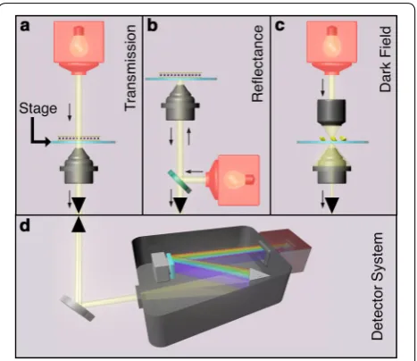
Methods Optical setup
The MExS setup (Fig. 1, and Additional file 1: Figure S1) consists of an inverted microscope system (Nikon Eclipse Ti), a piezoelectric stage (Physik Instrumente P-545.3C7), a spectrometer (Princeton Instruments IsoPlane SCT 320 equipped with a 50 grooves/mm grating), a 1024×1024 pixel array EMCCD camera (Princeton Instruments ProEM-HS: 1024BX3), an imaging camera (QImaging QIClick), a 12 V 100 W halogen lamp (Nikon D-LH/LC) for transmission and darkfield measurements, and an LED lamp (Lumen Dynamics X-Cite 120LED) for reflec-tance measurements. For scattering measurements, a dry darkfield condenser (Nikon, N.A. 0.95–0.80) is inserted in the optical path before the sample. The microscope is equipped with two objectives (Nikon CFI Plan Fluor 100XS Oil and Nikon CFI S Plan Fluor ELWD 40×) and an 80:20 beam splitter that sends 80% of the light to the spectrometer and 20% of the light to the imaging camera for simultaneous optical imaging and spectral measurements.
The dimensions of the acquired dataset depend on the spectrometer slit’s height and the stage’s range of motion (Table 1). The x dimension is defined by the slit height and scales with magnification (325 μm for the 40×, 140 μm for the 100× objective). The range of motion of the piezoelectric stage (here, 200 μm) defines the y dimension. The spatial resolution is diffraction limited, and the spectral resolution is defined by the choice of dis-persion grating.
Hyperspectral data acquisition
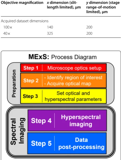
Figure 2 shows the five steps involved when performing MExS. Prior to spectral imaging, the optical setup is con-structed, and the sample is mounted onto the stage of the microscope. An image of the region of interest (ROI) is acquired using the imaging camera, creating a map used in data acquisition and analysis. The optical and hyper-spectral parameters are then set; example parameters are shown in Table 2. Next, hyperspectral imaging is initi-ated, and data are exported in comma-separated value (CSV) files. Finally, experiment-specific post-processing calculations (Table 3) are performed on the data.
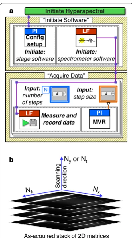
The operation of this hyperspectral spatial-scanning technique relies on communication between two compo-nents: the sample stage and the detector system (Fig. 1). This communication is established and manipulated through a LabVIEW control (LabVIEW block diagram in Fig. 3a, LabVIEW user interface in Additional file 1: Figure S2). At the onset of the experiment, the Lab-VIEW code enters the “Initiate Software” mode. Once both software programs have been initiated and a line of communication has been established, the user enters the spatial-scanning hyperspectral parameters (step size, number of steps Ny) into the LabVIEW user
inter-face. The user then advances the LabVIEW program into the “Acquire Data” mode; the detector and stage are manipulated in series to record data and move the sam-ple Ny times. At each step, the detector system records
2D matrix with a spatial dimension (Nx) and a spectral
dimension (Nλ), the lengths of which are defined by the
EMCCD chip size, where Nx= 1024 and Nλ= 1024. An
Ny stack of these 2D matrices creates an x–y–λ datacube
(Fig. 3b). The piezoelectric stage used here employs a closed-loop system that records with high-precision the actual displacement of the stage, eliminating any signifi-cant concerns of hysteresis or stage drift on the measure-ment timescale. All scanning is done in the y-dimension.
MExS can also be adapted for time-resolved studies, where time substitutes the y-axis, i.e., the stage remains immobile, and the detector records data for one row loca-tion (y) over time. In this setup, the user assigns the time-lapse parameters (number of time-time-lapse acquisitions, Nt,
Table 1 Acquired dataset dimensions for various objective magnifications
Objective magnification x dimension
(slit-length limited), μm yrange-of-motion dimension (stage limited), μm
Acquired dataset dimensions
100× 140 200
40× 325 200
Fig. 2 User process diagram describing MExS preparation (optical, hyperspectral) and spectral imaging (imaging and processing of data)
Table 2 Examples of optical and hyperspectral parameters to be set by the user prior to data acquisition
a Objective magnification: 40× and 100× respectively
b Only N
y or Nt is relevant in a given experiment
Optical parameters Hyperspectral parameters
Parameter Example Parameter Example
Exposure time 0.5 s Image width passed through slit 3.85 μma
Exposures/frame 4 1.54 μma
Grating grooves/mm 50 Step size 0.8 μm
Center wavelength 600 nm Number of steps (Ny)b 250
Number of time-lapse acquisitions (Nt)b 100 Acquisition frequency 10 s
Table 3 Examples of experiment-specific computations utilized in data post-processing
Technique Variable of interest Computation Example application
Transmission Absorption −log
Sample transmittance Direct transmittance
2D materials electronic properties
Reflectance Differential reflectance |Sample reflectance−Substrate reflectance|
Substrate reflectance 2D materials substrate interactions
Darkfield Scattering Particle scattering−Background scattering
and acquisition frequency), and a series of 2D matrices (Nx, Nλ) are recorded, leading to an x–λ–t—datacube (Nx,
Nλ, Nt).
Data post-processing
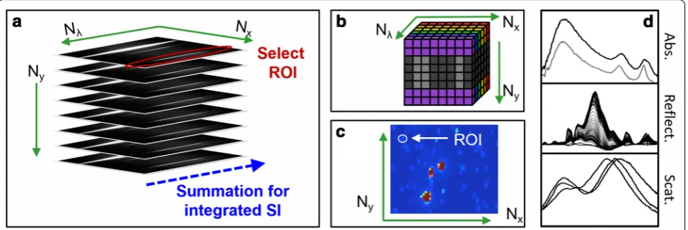
In the post-processing step (Fig. 4), the previously exported 2D matrices are imported into the Matlab-based
analysis software (code structure in Additional file 1: Fig-ure S3, code details available upon request). The datacube contains up to 1024 × 1024 ×Ny elements for
spatial-scanning experiments and 1024 × 1024 ×Nt elements for
time-lapse experiments. The datacube is first integrated along the λ dimension to create an integrated spectrum, resulting in a picture-like 2D x–y matrix (Fig. 4c). The pixel locations for each ROI are then determined using the integrated spectrum image. These pixel values are then used to extract the λ element values (point spec-tra) within the datacube corresponding to the selected ROI. An ROI usually covers several pixels, such that sev-eral point spectra in a square array around the center of the ROI are typically added together. Experiment-spe-cific computations (Table 3) are then conducted on the extracted data. The processed data are displayed (Fig. 4d) and written to CSV and Matlab workspace files.
Results and discussion
Three case studies are described below. For each, a brief background is followed by key findings to exemplify the scope of applicability of MExS.
Case study 1. Transmission characterization of 2D transition metal dichalcogenides
TMDs have recently gained much attention because of their potential applications in electronics [8–11] and optoelectronics [8, 12–14]. At monolayer thickness, TMDs can exhibit direct electronic and optical band-gaps ranging from the visible to the near-infrared. Opti-cal spectroscopy techniques such as photoluminescence (PL) and Raman are currently the key methods used in studying TMD properties such as bandgap energy, [15,
16] emission efficiency, [17–19] and defect density [19–
21]. However, PL and Raman spectroscopies have limited quantum efficiency, making them unfit for high-through-put applications. The already-limited PL emission effi-ciency decreases sharply with increasing defect density. Moreover, both require rather specialized instrumenta-tion [22, 23]. Because photons are absorbed regardless of the quenched PL emission, transmission MExS can over-come some of the yield limitations of PL, while providing simpler and faster operation than either PL or Raman.
MExS is a fast, large-scale approach to determine the optical bandgap energy and the extinction efficiency of TMDs. In this case study, MExS in transmission mode is used to identify and characterize monolayers of MoS2,
MoSe2, WS2, and WSe2 (Fig. 5). The samples were grown
by chemical vapor deposition on quartz coverslips based on previously published techniques [24–27]. An example of optical image and wavelength-integrated hyperspec-tral datacube (forming a 2D image) is shown in Fig. 5a, b, and the rest are shown in Additional file 1: Figure S4. Fig. 3 Data acquisition. a Block diagram depicting the hyperspectral
code design corresponding to the LabVIEW user interface (shown in Additional file 1: Figure S2). When the user selects the “start” button in the user interface, the code enters the “Initiate Software” mode, launching the software for both the piezoelectric stage (PI Physik Instrumente stage software) and the spectrometer (LF Lightfield, Princeton Instruments software for detector system). Once the parameters have been set for the experiment in the user interface and the user advances the code into the “Acquire Data” section, the code goes through N cycles of data acquisition and stage movement.
The exciton peaks of the different TMD monolayers arise from direct bandgap transitions (A and B) at the K point of the Brillouin zone (Fig. 5c). Since the different TMDs have different bandgap energies, the position of the exci-ton peaks provides an accessible way to identify each material.
Case study 2. Reflectance characterization of 2D materials on nontransparent substrates
MExS in reflectance mode provides additional charac-terization functionality, opening the door to the study of nontransparent materials inaccessible with transmit-tance. Typical growth substrates for TMDs and other 2D materials (e.g., Cu and Si wafer) are opaque, as are many electrode materials (TiN, C) and surfaces of interest for antiwear/anticorrosion coatings (steel and other metal alloys). In this case study, the interaction between WS2
and a TiN substrate was observed as an example of TMD behavior in corrosive environments, demonstrating the applicability of MExS to nontransparent substrates.
The samples used in this case study were prepared by using a micromechanical exfoliation technique that is described elsewhere [28]. The stacked layers of WS2 are
held together via van der Waals interactions, whereas the base layer is held to the TiN substrate via strong covalent bonds [28–31]. Various conditions were applied to these WS2/TiN samples in order to simulate corrosive
environ-ments. Because the bandgap of the bulk state and mon-olayer state of WS2 vary significantly (1.3 eV vs. 2.1 eV,
respectively), the exciton energy can be used to track the layer thickness, providing insight into the effects of cor-rosive environments [8].
The integrated spectrum images (Fig. 6a, b) are refer-enced against the corresponding optical images (Fig. 6c, d) to locate the region of interest (identified here by an arrow). The reflectance signal contains a feature related to an exciton at 646 nm for the multilayer thin film (Fig. 6e). This exciton blue shifts to 616 nm as the film reaches monolayer thickness as a result of corrosion. The use of reflectance-mode MExS offers an opportunity to study large TMD flakes and monitor corresponding sub-strate interactions efficiently with the flexibility afforded by the use of nontransparent substrates.
Case study 3. Darkfield scattering refractive index sensitivity of single gold nanoparticles: a sensitivity– structure correlation
MExS in scattering mode provides information about light–matter interactions in small scattering NPs. When light interacts with certain free-electron metal NPs (Au, Ag, Al, etc.), its electric field creates a collective electron oscillation called a localized surface plasmon resonance (LSPR) [32]. This resonance imparts bright colors and enhanced light–matter interaction properties to the NPs [33] and is dependent on NP size, shape, composition, and surrounding environment [34–36]. The latter can be used to construct plasmon sensors, as variations in the dielectric environment around the NP lead to approxi-mately linear changes in LSPR frequency [33]. A meas-ure of the sensing ability of a plasmonic system is the slope of the LSPR as a function of refractive index, i.e., the refractive index sensitivity (RIS) typically reported in nm per refractive index unit (nm/RIU) or eV/RIU. Val-ues have been reported for Au nanorods, stars, crescents, Fig. 4 Post-processing of acquired data. a As-acquired stack of 2D matrices. Integration along the Nλ-axis creates an integrated spectrum image
(SI) as shown in c. A point spectrum at a particular x,y-location can be extracted for the region of interest (ROI). b Representation of a raw datacube.
c Integrated spectrum image generated by summation along the Nλ-axis. This serves as a map in data post-processing. d Representative point
decahedra, bipyramids, and other shapes, and, together with the NP’s LSPR energy and stability, are critical design rules for plasmon sensors [37–41]. An even more powerful expression is the sensing figure of merit (FOM), [42] defined as the RIS divided by the LSPR full width at half maximum (FWHM) in eV, i.e.,
(1) FOM= RIS
FWHM
The FOM can be challenging to obtain because of heterogeneous broadening, requiring single NP meas-urements. In this case study, we show that MExS in scattering mode can easily provide the large statistics needed to extract RIS and FOM values at the single NP level, enabling detailed studies that are not blurred by the ensemble-averaging of bulk measurements.
Three different batches of Au decahedra were syn-thesized using a previously published one-pot polyol process that allows both size and shape controls [43]. NPs were drop-cast on transparent and conductive indium tin oxide (ITO)-coated coverslips. The cover-slips were marked with a scratch pattern for location reference. Coverslips were secured on a custom-built liquid cell and mounted on the microscope stage. The imaging camera was used to collect an optical map of the region of interest (Fig. 7a). Then, a MExS datacube was obtained for NPs submerged in solutions of varying refractive indices (water and glycerol; up to 70% glyc-erol), providing the single-particle darkfield scattering information needed to determine single-particle RIS. Representative data show the LSPR shift (Fig. 7c) as a function of RI, as well as the RIS (Fig. 7d) calculated from the slope of the linear relationship between the Fig. 5 Absorption spectra of different TMDs obtained by MExS. a
Optical image of a MoS2 flake. The clear parts of the structure show monolayers, and darker lines show multilayers. b Integrated spectrum image of the transmission intensity. The black square shows the location from where the spectrum was taken, shown in d. c Simplified schematic of the band diagram of MoS2, depicting c1 as the lowest conduction band, and v1 and v2 as the highest split valence bands. A and B are the direct bandgap transitions, which are the source of the two exciton resonances in the absorption spectrum. d Absorption spectra of MoS2, MoSe2, WS2, and WSe2; each labeled with exciton resonances A and B
LSPR peak energy of the NP vs. the refractive index of the medium [33].
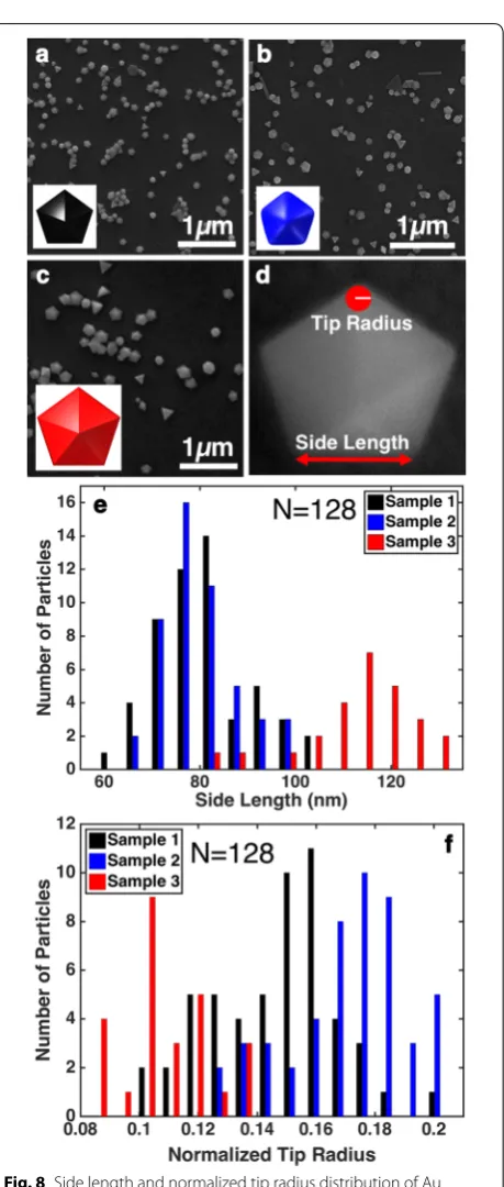
Each ROI from the hyperspectral datacube can further be investigated with scanning electron microscopy (SEM, Fig. 7e), revealing structure–property relationships; here, the size and shape effect on RIS and FOM is observed. A total of 128 NPs were studied in this fashion (Figs. 7, 8,
9). The size and shape of each NP was measured from its SEM image with ImageJ, an open-source image analysis software. Before correlating the structure and sensitivity of the NPs, we aimed to better understand the features of each of the three NP batches using the side length and tip radius as indicators; note that we report, for easier
Fig. 7 Single NP spectroscopy using darkfield MExS. a Optical image of the scattering of Au decahedra deposited on an ITO coverslip, showing proper distribution. The red circle indicates a NP of interest. b MExS reconstructed spectrum image of the ROI. The red circle indicates the same NP of interest, and the colormap shows the integrated scattering intensity from low (blue) to high (red). c
Darkfield scattering of a single NP in water–glycerol solutions with different refractive indices (n). d LSPR energy vs. refractive index for the data shown in c. The slope is the RIS of the single NP. e SEM image of the NP for which data are shown in c, d
comparison, the normalized tip radius, i.e., tip radius divided by side length [44]. As shown in Fig. 8, the three samples offer significant structure variety: NPs in samples 1 and 2 have similar side length but different tip radius, while NPs in sample 3 have larger side length and rela-tively small normalized radius (i.e., sharper tips). Specifi-cally, the average (standard deviation) side length was 81 (10), 80 (8), and 114 (12) for samples 1, 2, and 3, respec-tively; the average (standard deviation) normalized radius was 0.15 (0.02), 0.17 (0.02) and 0.109 (0.014) for samples 1, 2, and 3, respectively. From these structural variations emerge differences in LSPR properties. The LSPR energy, as expected, scales inversely with side length, i.e., LSPR energy is lower for bigger NPs (Additional file 1: Figure S5a) [1]. Interestingly, NPs in samples 1 and 2 have simi-lar side lengths yet different LSPR energies because of the blue-shifting effect of corner rounding [44]. Lastly, NPs
in samples 1, 2, and 3 show a common trend as a func-tion of tip radius, with rounder NPs having a higher LSPR energy (Additional file 1: Figure S5b).
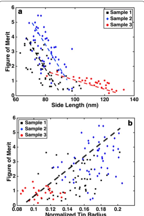
Correlation of the structural parameters, at the sin-gle NP level, and the ability to obtain FWHM that are not heterogeneously broadened provides insight on structure–property relationships. MExS/SEM analysis reveals that both RIS and FOM are greatest for small NPs (Additional file 1: Figure S6a and Fig. 9a, respec-tively). Samples 1 and 2 show large variance in RIS and FOM for NPs of comparable size, which can be attrib-uted to corner rounding effects. A trend is again found by using normalized tip radius as the structural param-eter, where rounder NPs are more sensitive and have higher FOM (Additional file 1: Figure S6b and Fig. 9b). These results indicate that side length is not the only structural parameter to be considered when identifying NPs suitable for sensing applications; the normalized tip radius appears to be a unifying structural parameter. Such study, requiring statistical information on many single NPs and multiple measurements (in different solutions) for each NP has uniquely been enabled by the high-throughput capabilities of MExS and provides useful guidelines for NP selection in the design of label-free (bio)sensors.
Conclusions
We described a hyperspectral tool suitable for nanoma-terials’ characterization. The automation of the system’s hardware and software relies on LabVIEW, and a Mat-lab-based analysis s interface was developed for the data post-processing. We presented three different case stud-ies that use the different optical modes in MExS. First, by applying the transmission mode, different TMDs were identified quickly and without the need for lasers, tak-ing advantage of the line-scanntak-ing operation of MExS. Next, by applying the reflectance mode, the interaction between WS2 flakes and a TiN substrate was studied.
Finally, the optical sensitivity of Au NPs was determined by studying their scattering under different liquid media. We are convinced that MExS is not only effective in the described examples, but can also be used in chemical/ biological in situ experiments, thin film and coating anal-ysis, or in situ catalytic mechanism studies.
Author’s contributions
AK developed the data acquisition and data analysis software, and performed the reflectance case study. EV designed optical setups and performed the transmission and darkfield case studies. ER designed the research. All authors Additional file
Additional file 1. Additional figures. Fig. 9 Structure–sensitivity correlation conducted by using MExS
contributed equally to the writing of the paper. All authors read and approved the final manuscript.
Author details
1 Department of Chemistry, Rice University, Houston, TX, USA. 2 Department
of Materials Science and Nanoengineering, Rice University, Houston, TX, USA.
3 Department of Materials Science and Metallurgy, University of Cambridge,
Cambridge, UK. 4 Department of Earth Sciences, University of Cambridge,
Cambridge, UK.
Acknowledgements
The authors acknowledge P.M. Ajayan and X. Zhang for providing samples used in Case Study 1, and S. Das, A. Sebastian, and V. Huang for collaborations in the electrochemical design of Case Study 2.
Competing interests
The authors declare that they have no competing interests.
Availability of data and materials Data and material available upon request.
Funding
This research was supported by the Air Force Office of Scientific Research Grant no. AFOSR-YIP FA9550-17-0202, the Binational Science Foundation Grant no. 2016149, and the NSF I/UCRC ATOMIC. E. V. acknowledges the National Sci-ence Foundation Graduate Research Fellowship (Grant 0940902). This research made use of instruments in the Shared Equipment Authority at Rice University.
Publisher’s Note
Springer Nature remains neutral with regard to jurisdictional claims in pub-lished maps and institutional affiliations.
Received: 27 February 2018 Accepted: 4 July 2018
References
1. Kelly, K.L., Coronado, E., Zhao, L.L., Schatz, G.C.: The optical properties of metal nanoparticles: the influence of size, shape, and dielectric environment. J. Phys. Chem. B. 107(3), 668–677 (2003). https ://doi. org/10.1021/jp026 731y
2. Bhimanapati, G.R., Lin, Z., Meunier, V., Jung, Y., Cha, J., Das, S., Xiao, D., Son, Y., Strano, M.S., Cooper, V.R., Liang, L., Louie, S.G., Ringe, E., Zhou, W., Kim, S.S., Naik, R.R., Sumpter, B.G., Terrones, H., Xia, F., Wang, Y., Zhu, J., Akinwande, D., Alem, N., Schuller, J.A., Schaak, R.E., Terrones, M., Rob-inson, J.A.: Recent advances in two-dimensional materials beyond gra-phene. ACS Nano 9(12), 11509–11539 (2015). https ://doi.org/10.1021/ acsna no.5b055 56
3. Ringe, E., Sharma, B., Henry, A.-I., Marks, L.D., van Duyne, R.P.: Single nanoparticle plasmonics. Phys. Chem. Chem. Phys. 15(12), 4110–4129 (2013). https ://doi.org/10.1039/c3cp4 4574g
4. Boldrini, B., Kessler, W., Rebnera, K., Kessler, R.W.: Hyperspectral imag-ing: a review of best practice, performance and pitfalls for in-line and on-line applications. J. Near Infrared Spectrosc. 20(5), 483–508 (2012). https ://doi.org/10.1255/1003
5. Chang, C.: Hyperspectral imaging: techniques for spectral detection and classification, 1st edn. Springer, US (2003)
6. Bingham, J.M., Willets, K.A., Shah, N.C., Andrews, D.Q., van Duyne, R.P.: Localized surface plasmon resonance imaging: simultaneous single nanoparticle spectroscopy and diffusional dynamics. J. Phys. Chem. C 113(39), 16839–16842 (2009). https ://doi.org/10.1021/jp907 377h 7. Byers, C.P., Hoener, B.S., Chang, W.S., Yorulmaz, M., Link, S., Landes, C.F.:
Single-particle spectroscopy reveals heterogeneity in electrochemi-cal tuning of the loelectrochemi-calized surface plasmon. J. Phys. Chem. B. 118(49), 14047–14055 (2014). https ://doi.org/10.1021/jp504 454y
8. Wang, Q.H., Kalantar-Zadeh, K., Kis, A., Coleman, J.N., Strano, M.S.: Electron-ics and optoelectronElectron-ics of two-dimensional transition metal dichalcoge-nides. Nat. Nanotechnol. 7(11), 699–712 (2012). https ://doi.org/10.1038/ nnano .2012.193
9. Bablich, A., Pawar, R., Iannaccone, G., Downing, C., Fiori, G., Lemme, M.C., Duesberg, G.S.: Heterojunction hybrid devices from vapor phase grown MoS2. Sci. Rep. 4, 4–10 (2014). https ://doi.org/10.1038/srep0 5458 10. Lembke, D., Bertolazzi, S., Kis, A.: Single-layer MoS2 electronics. Acc. Chem.
Res. 48, 100–110 (2015). https ://doi.org/10.1021/ar500 274q 11. Langouche, L., Kamalakar, M.V., Dash, S.P.: High-performance
molybde-num disulfide field-effect transistors with spin tunnel contacts. ACS Nano 8(1), 476–482 (2014). https ://doi.org/10.1021/nn404 961e
12. Atwater, H.A.: Near-unity absorption in van der Waals semiconductors for ultrathin optoelectronics. Nano Lett. 16, 5482–5487 (2016). https ://doi. org/10.1021/acs.nanol ett.6b019 14
13. Pospischil, A., Mueller, T.: Optoelectronic devices based on atomically thin transition metal dichalcogenides. Appl. Sci. 6, 1–20 (2016). https ://doi. org/10.3390/app60 30078
14. Mak, K.F., Shan, J.: Photonics and optoelectronics of 2D semiconductor transition metal dichalcogenides. Nat. Photonics 10(4), 216–226 (2016). https ://doi.org/10.1038/nphot on.2015.282
15. Mak, K.F., Lee, C., Hone, J., Shan, J., Heinz, T.F.: Atomically thin MoS2: a new direct-gap semiconductor. Phys. Rev. Lett. 105(13), 2–5 (2010). https :// doi.org/10.1103/PhysR evLet t.105.13680 5
16. Wang, B.B., Ostrikov, K., Van Der Laan, T., Zheng, K., Shao, R., Zhu, M.K., Zou, S.S.: Growth and photoluminescence of oriented MoSe2 nanosheets pro-duced by hot filament CVD. RSC Adv. 6(43), 37236–37245 (2016). https :// doi.org/10.1039/c6ra0 5737c
17. Plechinger, G., Nagler, P., Arora, A., Schmidt, R., Chernikov, A., Lupton, J., Bratschitsch, R., Schüller, C., Korn, T.: Valley dynamics of excitons in monolayer dichalcogenides. Phys. Status Solidi Rapid Res. Lett. 11(7), 1–6 (2017). https ://doi.org/10.1002/pssr.20170 0131
18. Plechinger, G., Nagler, P., Arora, A., Granados Del Águila, A., Ballottin, M.V., Frank, T., Steinleitner, P., Gmitra, M., Fabian, J., Christianen, P.C.M., Bratschitsch, R., Schüller, C., Korn, T.: Excitonic valley effects in monolayer WS2 under high magnetic fields. Nano Lett. 16(12), 7899–7904 (2016). https ://doi.org/10.1021/acs.nanol ett.6b041 71
19. Feierabend, M., Morlet, A., Berghäuser, G., Malic, E.: Impact of strain on the optical fingerprint of monolayer transition-metal dichalcogenides. Phys. Rev. B. 96(4), 1–7 (2017). https ://doi.org/10.1103/PhysR evB.96.04542 5 20. Lin, Z., Carvalho, B.R., Kahn, E., Lv, R., Rao, R., Terrones, H., Pimenta,
M.A., Terrones, M.: Defect engineering of two-dimensional transi-tion metal dichalcogenides. 2D Mater. 3(2), 22002 (2016). https ://doi. org/10.1088/2053-1583/3/2/02200 2
21. Carozo, V., Wang, Y., Fujisawa, K., Carvalho, B.R., McCreary, A., Feng, S., Lin, Z., Zhou, C., Perea-López, N., Elías, A.L., Kabius, B., Crespi, V.H., Terrones, M.: Optical identification of sulfur vacancies: bound excitons at the edges of monolayer tungsten disulfide. Sci. Adv. 3(4), e1602813 (2017). https ://doi. org/10.1126/sciad v.16028 13
22. Amani, M., Lien, D.-H., Kiriya, D., Xiao, J., Azcatl, A., Noh, J., Madhvapathy, S.R., Addou, R., Kc, S., Dubey, M., Cho, K., Wallace, R.M., Lee, S.-C., He, J.-H., Ager, J.W., Zhang, X., Yablonovitch, E., Javey, A.: Near-unity photolumi-nescence quantum yield in MoS2. Science 350(6264), 1065–1068 (2015). https ://doi.org/10.1126/scien ce.aad21 14
23. Amani, M., Taheri, P., Addou, R., Ahn, G.H., Kiriya, D., Lien, D.H., Ager, J.W., Wallace, R.M., Javey, A.: Recombination kinetics and effects of superacid treatment in sulfur- and selenium-based transition metal dichalcoge-nides. Nano Lett. 16(4), 2786–2791 (2016). https ://doi.org/10.1021/acs. nanol ett.6b005 36
24. Gong, Y., Ye, G., Lei, S., Shi, G., He, Y., Lin, J., Zhang, X., Vajtai, R., Pantelides, S.T., Zhou, W., Li, B., Ajayan, P.M.: Synthesis of millimeter-scale transi-tion metal dichalcogenides single crystals. Adv. Funct. Mater. 26(12), 2009–2015 (2016). https ://doi.org/10.1002/adfm.20150 4633
25. Gong, Y., Lei, S., Ye, G., Li, B., He, Y., Keyshar, K., Zhang, X., Wang, Q., Lou, J., Liu, Z., Vajtai, R., Zhou, W., Ajayan, P.M.: Two-step growth of two-dimen-sional WSe2/MoSe2 heterostructures. Nano Lett. 15(9), 6135–6141 (2015). https ://doi.org/10.1021/acs.nanol ett.5b024 23
26. Gong, Y., Lin, J., Wang, X., Shi, G., Lei, S., Lin, Z., Zou, X., Ye, G., Vajtai, R., Yakobson, B.I., Terrones, H., Terrones, M., Tay, B.K., Lou, J., Pantelides, S.T., Liu, Z., Zhou, W., Ajayan, P.M.: Vertical and in-plane heterostructures from WS2/MoS2 monolayers. Nat. Mater. 13(12), 1135–1142 (2014). https ://doi. org/10.1038/nmat4 091
of crystalline monolayer MoSe2. ACS Nano 8(5), 5125–5131 (2014). https ://doi.org/10.1021/nn501 175k
28. Das, S., Bera, M.K., Tong, S., Narayanan, B., Kamath, G., Mane, A., Paulikas, A.P., Antonio, M.R., Sankaranarayanan, S.K.R.S., Roelofs, A.K.: A self-limiting electro-ablation technique for the top–down synthesis of large-area monolayer flakes of 2D materials. Sci. Rep. 6, 28195 (2016)
29. Bewilogua, K., Hofmann, D.: History of diamond-like carbon films—from first experiments to worldwide applications. Surf. Coatings Technol. 242, 214–225 (2014). https ://doi.org/10.1016/j.surfc oat.2014.01.031 30. Montemor, M.F.: Functional and smart coatings for corrosion protection:
a review of recent advances. Surf. Coatings Technol. 258, 17–37 (2014). https ://doi.org/10.1016/j.surfc oat.2014.06.031
31. Singh, B.P., Jena, B.K., Bhattacharjee, S., Besra, L.: Development of oxidation and corrosion resistance hydrophobic graphene oxide-polymer compos-ite coating on copper. Surf. Coatings Technol. 232, 475–481 (2013). https ://doi.org/10.1016/j.surfc oat.2013.06.004
32. Sriram, M., Zong, K., Vivekchand, S.R., Justin, G.J.: Single nanoparticle plasmonic sensors. Sensors 15(10), 25774–25792 (2015). https ://doi. org/10.3390/s1510 25774
33. Mayer, K.M., Hafner, J.H.: Localized surface plasmon resonance sensors. Chem. Rev. 111(6), 3828–3857 (2011). https ://doi.org/10.1021/cr100 313v 34. Liz-Marzán, L.M.: Tailoring surface plasmons through the morphology and
assembly of metal nanoparticles. Langmuir 22(1), 32–41 (2006). https :// doi.org/10.1021/la051 3353
35. Ringe, E., McMahon, J.M., Sohn, K., Cobley, C., Xia, Y., Huang, J., Schatz, G.C., Marks, L.D., van Duyne, R.P.: Unraveling the effects of size, composition, and substrate on the localized surface plasmon resonance frequencies of gold and silver nanocubes: a systematic single-particle approach. J. Phys. Chem. C 114(29), 12511–12516 (2010). https ://doi.org/10.1021/jp104 366r 36. Haes, A.J., Van Duyne, R.P.: A unified view of propagating and localized
surface plasmon resonance biosensors. Anal. Bioanal. Chem. 379(7–8), 920–930 (2004). https ://doi.org/10.1007/s0021 6-004-2708-9
37. Chen, H., Kou, X., Yang, Z., Ni, W., Wang, J.: Shape-and size-dependent refractive index sensitivity of gold nanoparticles. Langmuir 31, 5233– 5237 (2008). https ://doi.org/10.1021/la800 305j
38. Bocchio, N.L., Unger, A., Alvarez, M., Kreiter, M.: Thin layer sensing with multipolar plasmonic resonances. J. Phys. Chem. C 112(37), 14355–14359 (2008). https ://doi.org/10.1021/jp804 099u
39. Nehl, C.L., Liao, H., Hafner, J.H.: Optical properties of star-shaped gold nanoparticles. Nano Lett. 6(4), 683–688 (2006). https ://doi.org/10.1021/ nl052 409y
40. Myroshnychenko, V., Nelayah, J., Adamo, G., Geuquet, N., Rodríguez-Fernández, J., Pastoriza-Santos, I., MacDonald, K.F., Henrard, L., Liz-Marzán, L.M., Zheludev, N.I., Kociak, M., García De Abajo, F.J.: Plasmon spectros-copy and imaging of individual gold nanodecahedra: a combined optical microscopy, cathodoluminescence, and electron energy-loss spectros-copy study. Nano Lett. 12(8), 4172–4180 (2012). https ://doi.org/10.1021/ nl301 742h
41. Lee, K.S., El-Sayed, M.A.: Gold and silver nanoparticles in sensing and imaging: sensitivity of plasmon response to size, shape, and metal composition. J. Phys. Chem. B. 110(39), 19220–19225 (2006). https ://doi. org/10.1021/jp062 536y
42. Shin, Y.J., Ringe, E., Personick, M.L., Cardinal, M.F., Mirkin, C.A., Marks, L.D., Van Duyne, R.P., Hersam, M.C.: Centrifugal shape sorting and optical response of polyhedral gold nanoparticles. Adv. Mater. 25(29), 4023–4027 (2013). https ://doi.org/10.1002/adma.20130 1278
43. Seo, D., Yoo, C.I., Chung, I.S., Seung, M.P., Seol Ryu, A., Song, H.: Shape adjustment between multiply twinned and single-crystalline polyhedral gold nanocrystals: decahedra, icosahedra, and truncated tetrahedra. J. Phys. Chem. C (2008). https ://doi.org/10.1021/jp710 9498