ISSN: 2231-5381
http://www.ijettjournal.org
Page 1325Design of an Amplifier through Second Generation
Current Conveyor
Nikhita Tripathi*1, Nikhil Saxena *2, Sonal Soni*3
*123PG scholars
Department of Electronics & communication, Jaypee Institute of Information Technology Noida
Abstract: - This paper describes the architecture of first and second generation current conveyor (CCI and CCII respectively) and designing an amplifier using second generation current conveyor. The designed amplifier through CCII+ can be used in various analog computation circuits and is superior in performance than the classical opamp. It provides better gain with higher accuracy.
Key words: CCI, CCII, Amplifier, CCII+.
I. INTRODUCTION
There have been significant advances in the last decades in
linear analog integrated circuit applications, since the
appearance of the operational amplifier. The applications of
opamp range from data converters to voltage references,
analog multipliers, wave shaping circuits, oscillators and
function generators. However, the classical op-amp suffers
from limited gain-bandwidth product problems and from low
slew rate at its output. They remain therefore unsatisfactory at
higher frequencies. Current-mode circuits are used instead of
voltage-mode circuits for a wide variety of applications.
Current-mode does not need high voltage gain and high
precision passive components, so they can be designed almost
entirely with transistors. Specifically a current conveyor can
provide a higher voltage gain over a larger signal bandwidth
under small or large signal conditions than a corresponding
op-amp circuit in effect a higher gain-bandwidth product.
Operational transconductance amplifiers (OTAs) can be used to perform the tuning but they suffer from limited output
voltage swing and temperature sensitivity. Therefore, current
conveyors are widely used.
From their introduction in 1968 by Smith and Sedra [1] and
subsequent reformulation in 1970 current conveyors [2] have
proved to be functionally flexible and versatile, rapidly
gaining acceptance as both a theoretical and practical building
block like filters, oscillators and amplifiers. In addition, a
number of novel circuit functions and topologies have been
explored. In many ways the current conveyor simplifies
design in much as the same manner as the conventional
operational amplifier (op-amp). Current-mode circuits have
received significant attention due to their advantages
compared to voltage mode circuits in terms of inherently wide
bandwidth, greater linearity, wide dynamic range, simple
circuitry and lower power consumption [3-4].
II.CURRENT MODE Vs VOLTAGE MODE SIGNALS
There are several good reasons why current mode signals
should be considered. Although errors can be introduced into
any signal, voltage mode signals are susceptible to more than
ISSN: 2231-5381
http://www.ijettjournal.org
Page 1326 These include the impedance of the voltage source and
other supply fluctuations, wire and connection
resistance, the integrity of wire insulation, electrostatic
and electromagnetic noise, and ground potential
differences. Care must be taken not to load a voltage
signal as new devices are added.
The only real advantage of voltage mode signals is that they interface directly with D/A and A/D
converters and analog multiplexing devices.
Current mode signals are immune to loop resistance
found in long wire runs and faulty connections.
Additional devices generally can be added to the loop
without concern for the signal, supply permitting.
Current mode signals are relatively immune to noise,
the only exception being electromagnetically induced
noise which can be substantially eliminated through
the proper use of shielded twisted pairs.
III. EARLY DEVELOPMENTS
Current conveyors were first developed by Smith and
Sedra(1990). The second-generation current conveyor (CCII)
was developed shortly thereafter [6].
III-A.FIRST GENERATION CURRENT-CONVEYOR
(CCI)
The concept of the current-conveyor was first presented in
1968. The current-conveyor is intended as a general building
block as with the operational amplifier [7]. Because of the
operational amplifier concept has been current since the late 1940’s, it is difficult to get any other similar concept widely
accepted. However, operational amplifiers do not perform
well in applications where a current output signal is needed
and consequently there is an application field for
current-conveyor circuits. Since current-current-conveyors operate without
any global feedback, different high frequency behavior
compared to operational amplifier circuits results.
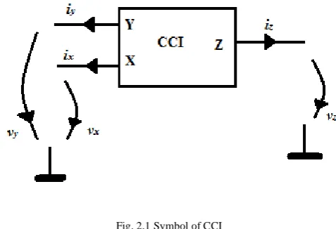
Fig. 2.1 Symbol of CCI
Current-conveyors are three-port networks with terminals X,
Y and Z as represented in Figure 2.1. The network of the first
generation current-conveyor CCI has been formulated in a
matrix form as follows:
Z X Y Z X YV
I
V
I
V
I
0
1
0
0
0
1
0
1
0
In other words, the first generation current conveyor CCI
forces both the currents and the voltages in ports X and Y to
be equal and a replica of the currents is mirrored (or
conveyed) to the output port Z. The voltages at the terminals
X and Y are forced to be identical. Thus the device exhibits a
virtual short-circuited input characteristic at port X and a dual
virtual open-circuit input characteristic at port Y.
III-B. THE SECOND GENERATION CURRENT
CONVEYOR (CCII)
The second-generation current-conveyor was developed by
Sedra in 1970. A current conveyor is a building block similar
to an operational amplifier and which, when used in
ISSN: 2231-5381
http://www.ijettjournal.org
Page 1327 capacitors and diodes, can implement several useful analogsub-systems such as amplifiers, integrators, and rectifiers.
The second generation current conveyor is a three terminal
device. Its symbol is shown in figure 3.1.
Fig 3.1 Current Conveyor Symbol and Characteristic
The current conveyor's response is given by equation
Z X Y
Z X Y
V
I
V
I
V
I
0
0
0
0
1
0
0
0
Impedance is finite and must be taken into consideration in
the circuit design. When a voltage is applied at node Y, that
voltage is replicated at node X. This is similar to the virtual
short on an op-amp. Also when a current is injected into node
X, that same current gets copied into node Z. The notation
CCII+ denotes a positive Z output current conveyor (
= +1)whereas CCII- denotes a negative Z output current conveyor
(
=-1). Thus the terminal Y exhibits infinite inputimpedance. The voltage at X follows that applied to Y, thus X
exhibits zero input impedance. The current supplied to X is
conveyed to the high impedance output terminal Z where it is
supplied with either positive polarity (in CCII+) or negative
polarity (in CCII-). One model used to analyze a CCII+ is
shown in figure3.2. The op-amp in unity-gain feedback
configuration ensures that Vx is equal to Vy,and the current
mirrors ensure that Izis equal to IX. Here the op-amp's output
stage has infinite output impedance.
Fig 3.2 Mode1 for CCII+
A CCII- is obtained from a CCII+ by adding two current
mirrors in the output stage, inverting the output current, as
depicted in figure 3.4
ISSN: 2231-5381
http://www.ijettjournal.org
Page 1328Fig 3.4 Model for CCII
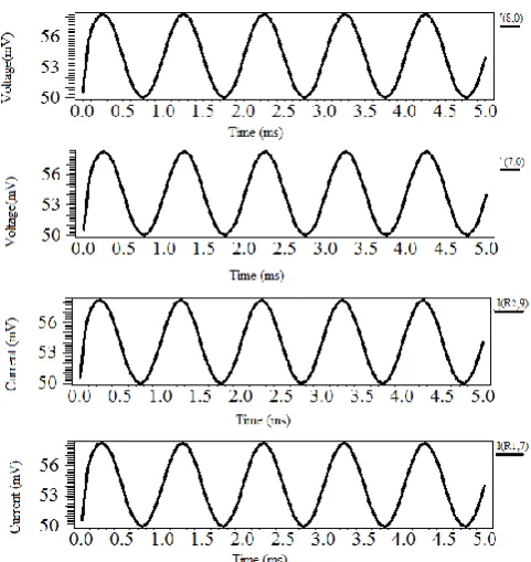
Fig. 3.5 Output waveform showing that Vx=Vy and ix=iz
IV. CMOS Implementation of CCC-II
The current controlled current conveyor (CCCII). It exhibits
the same features of the CCII plus the controllability. It has
been realized in different technologies, BJT, CMOS, and
BICMOS [1-5]. At present, there is a growing interest in
using the CCCII in various analogue signal processing
applications [6-10].
Fig 4.1 CMOS implementation of CCC-II
As a general rule, a current controlled conveyor CCCII is a
translinear CCII to which the possibility of modifying the
value of the DC bias current Ib will confer additional
properties. All the other characteristics of the CCIIs are
preserved. In order to underline the advantages of the use of
the controlled conveyors described here, we will compare its
performance with the conventional bipolar operational
transconductance amplifier (OTA) For OTA the value of
gm=I/(2Vt). Comparing this value with I/R, deduced from it
can be seen that for the same value of I, the transconductance
of the bipolar OTA will be four times less than that of the
CCCII. Thus, for the same transconductance the power
consumption of the bipolar OTA will be about three time
greater than with the CCCII. Second, with very high values for the collector currents of the transistors, the maximum
usable frequency of the OTA will be reached sooner. This
consequently indicates that the frequency performance of
circuits with controlled conveyors will be much better than
that for OTA implementations.
When signals are widely distributed as voltages, the parasitic
capacitancesare charged and discharged with the full voltage
swing, which limits the speed and increases the power
consumption of voltage-mode circuits. Current-mode circuits
ISSN: 2231-5381
http://www.ijettjournal.org
Page 1329 are usually local nodes with less parasitic capacitances.Therefore, it is possible to reach higher speed and lower
dynamic power consumption with current-mode circuit
techniques.
Current-mode interconnection circuits in particular show
promising performance. When the signal is conveyed as a
current, the voltages in MOS-transistor circuits are
proportional to the square root of the signal, if saturation
region operation is assumed for the devices. Similarly, in
bipolar transistor circuits the voltages are proportional to the
logarithm of the signal. Therefore, a compression of voltage
signal swing and a reduction of supply voltage is possible.
This feature is utilized for example in log-domain filters,
switched current filters, and in non-linear current-mode
circuits in general.
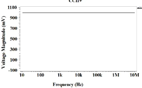
The diagram of CCII+ is shown in figured4.2 with the nodes
markad. Simulation results from SPICE tool have been shown
in figure 3.3, 3.5, 4.3, 4.5. CCII+ is used as an amplifier as
shown in figure 4.4. The ratio of R2 and R1 gives the gain of
the amplifier.
1 2
,
R
R
V
V
A
gain
IN OUT
V
Fig 4.2 Diagram of CCII+
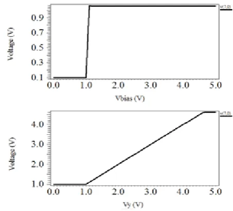
Fig. 4.3 From the transconductance curve we set the biasing point so that the transistors are in saturation.
Fig 4.4 CCII as an amplifier
ISSN: 2231-5381
http://www.ijettjournal.org
Page 1330 V.CONCLUSIONCurrent-mode circuits are undoubtedly the most widely
accepted operational devices in continuous time and current
mode signal processing. In addition a number of novel circuit
functions such as amplifier, integrator, summer, differentiator,
etc. and topologies like filters and oscillator have been
explored on a front of current mode analogue circuits, opening
up wider area of interest.
The circuit of CCII+ is verified through TSPICE simulation
results. The circuit of CCII+ and the designed amplifier is
verified through TSPICE simulationresults.
REFERENCES
[1] K. Smith and A. Sedra, ‘The Current Conveyor-a new circuit building block,’ IEEE Proc., vol. 56, pp. 1368-1369, 1968.
[2] A. Sedra, K. C. Smith, ‘A second generation current conveyor and its application’, IEEE Trans. Circuit Theory,pp. 132-134, 1970.
[3] C. Toumazou, F. J. Lidgey, and D. G. Haigh, ‘Analogue IC design: the current-mode approach’, London: Peter Peregrinus, 1990.
[5] Wilson. B, ‘Analogue current-mode circuits’, Int. J. Electr. Eng. Educ., 1989, 26, pp. 206-233
[6] Kumar. U, ‘Current conveyors: a review of the state of the art’, IEEE Circuits and Syst. Mag., 1981, 3, pp.10-14
[8] Fabre, A, ‘Third-generation current conveyor: A new helpful active element’, Elec. Letters, Vol. 31, No.5, pp. 338-339, Mar. 1995
[9] Wilson, B, ‘A new look at gain-bandwidth product’, Electron. Wirel. World, 1987,93, pp. 834-836