http://www.gjaets.com © Global Journal of Advance Engineering Technology and Sciences 33
Global Journal of Advanced Engineering Technologies and Sciences
COMPARATIVE STUDIES ON THE MORPHOLOGICAL AND
STRUCTURAL PROPERTIES OF SILAR DEPOSITED COPPER OXIDE
THIN FILM ON GLASS AND STAINLESS STEEL SUBSTRATES
Daniel-Umeri
*1, Rita and K. Emumejaye
2*1Delta State Polytechnic, Ozoro, Delta State, Nigeria.
Abstract
Copper oxide thin films have been deposited on glass and stainless steel substrates by using a simple, safe and environmental friendly chemical solution method known as successive ionic layer adsorption reaction (SILAR). The films were prepared by successively dipping them for 20s each in a solution of 1 M NaOH and then in a solution of 0.1M copper complex. Temperature of the NaOH solution was 700C, while that of the copper complex solution with ( pH 8- 12) was maintained at room temperature. The films were characterized by X-ray diffraction (XRD), Energy dispersive X-ray analysis (EDAX) and scanning electron microscopy (SEM)
The XRD measurements showed that formation of CuO nanostructures on glass substrates are more crystalline than that are on stainless steel substrates. SEM images reveals that the grain sizes of the CuO nanostructures deposited on stainless steel were larger than films deposited on glass substrate. Copper oxide films deposited using glass substrates showed a better morphology, higher crystallinity and better percentage ratio of the Cu/O composition than films deposited on stainless steel substrates.
Keywords:Copper oxide, SILAR method, Substrates, Structural properties.
Introduction
The growing interest in the research for Cuprous oxide ( Cu2O) nanostructures is due to the natural abundance of its
constituents; which is copper(Cu) and oxygen(o) , its potential as a photovoltaic material with lower cost, and as well as its non-toxicity [1],[2].
Depending on the growth method and parameters, reports shows that the deposition of cuprous oxide result in a combined growth of copper ( I ) oxide Cu2O and copper(II) oxide CuO .
Cuprous oxide belongs to group I–VI semiconductor with P-type conductivity, its band gap is in the range of about 1.9–2.2 eV . It has a cubic structure which makes it a promising material for solar cell applications [3], [4]
Cupric oxide (CuO) on the other hand, is the higher oxide of copper. As a mineral, it is known as tenorite and its band gap is in the range of 1.3–2.1 eV [6],[7],[[8],[9],[10],[11]. It belongs to the monoclinic crystal system, and its lattice parameters are a = 4.6837(5), b = 3.4226(5), c = 5.1288(6), α = 90°, β = 99.54(1)°, γ = 90° [12].
The discovery of carbon nanotubes by Iijima [13] has led to the growing interest in nanoscaled one-dimensional (1D) and two-dimensional (2D) materials such as nanoribbons [14] nanowires[15],[16],17], nanosheets [18] and nanorods [19]. These nanomaterials have attracted much attentions due to their unique optical,electrical and magnetic properties and their potential applications in nanodevices [20].
In recent years, copper-oxide-based nanostructures have found applications in various areas including heterogeneous catalysis [21], electrodes in dye-sensitized solar cells [22] and [23], biosensors [24]. Capacitors[25] semiconductors[26] field effect transistors [27] magnetic storage media [28] humidity sensors [29] batteries [30], anode materials for lithium-ion batteries [31], and antimicrobials [32]
http://www.gjaets.com © Global Journal of Advance Engineering Technology and Sciences 34
with thermal annealing [44] , electrochemical [45], sol–gel [46], thermal evaporation [47], pulsed laser deposition [48] sonochemical methods [49] and modified chemical bath method[50] ,[51] .
The method adopted in this work is the successive ionic layer adsorption and reaction (SILAR). It is relatively new and less investigated method for the deposition of metal chalcogenide thin films. SILAR method was first recorded as being used in 1985 in a laboratory environment, with the name SILAR first used in scientific journals of the same year, according to the Indian Academy of Sciences. It is based on the immersion of substrate into the separately placed anionic and cationic precursors and rinsing between every immersion in distilled water to avoid homogeneous precipitation.
In this method, when a substrate is immersed in cationic precursor, cations are adsorbed on the substrate surface, rinsing the substrate in distilled water can separate the unadsorbed or excess ions out and avoid homogeneous precipitation. When this substrate is immersed in anionic precursor solution, anions react with preadsorbed cations. The unreacted or powdery material can be removed by rinsing the substrate again in distilled water. These steps may be termed as one complete cycle. After repeating such appropriate cycles, multilayer film formation of appropriate thickness takes place.
Quality and thickness of the film mainly depend upon preparative parameters. In SILAR method, deposition of sufficiently thick film requires many hours and hence can be operated with microprocessor or computer.
The main advantages and interesting features of the SILAR deposition method include the ease of completing the method and the relative low cost.
When using the SILAR method, quality of the precursor solutions, composition, temperature complexing agent, their pH values, concentrations, adsorption and reaction time are among the main parameters that influence the film growth [53].
Mitra,(2010) [54] studied polycrystalline copper oxide thin films using successive ionic layer adsorption and reaction (SILAR) technique. He observed that for lower concentrations of copper sulphate complex, mixed phase of CuO and Cu2Owas
found. Pure phase of Cu2Owas observed
with enhanced concentration of copper sulphate complex.
Copper oxide prepared by electrochemical deposition was also reported by Richardson et al., (2000) [3]. The electrodeposited cuprous oxide obtained was a p-type semiconductor with a direct band gap of 2.06 eV, and on varying the pH range from 7.5 to 12.0, three different preferred crystal orientations: (100), (110) and (111) were obtained
Ahirrao et al., (2011) [51] reported the synthesis and photoluminescence properties of Copper oxide(Cu2O) thin film.
The Cu2O thin films were synthesized on amorphous glass substrate by using simple chemical route namely modified
chemical bath Deposition (M-CBD) method at room temperature. Crystallization and growth processes obtained
micro-spherical shaped grains Cu2O due to agglomeration of smaller nano-particles.
The diffraction pattern of XRD shows two dominant peaks at 36.2o and 42.2o corresponding to the (111) and (200)
planes of Cu2O are seen with cubic crystal structure. The average crystallite size is approximately 20 nm.
Cupric oxide has also been synthesized using a simple, low temperature and cost effective solution method by Bayansal et al., (2011) [55]. The CuO nanostructures obtained had high crystallinity and a monoclinic crystal structure in (-111) and (111) planes.
Nanostructured copper oxide films were prepared via sol–gel starting from ethanolic solutions of copper (II) acetate [Cu(CH3COO)2·H2O] was studied by Armelao et al., (2003) [56]. Films were obtained by dip-coating at room
http://www.gjaets.com © Global Journal of Advance Engineering Technology and Sciences 35
(N2) or reducing (4% H2 in N2) atmospheres. The evolution of the oxide coatings under thermal treatment was studied
by glancing incidence X-ray diffraction, X-ray photoelectron spectroscopy and X-ray excited Auger electron spectroscopy.
Different crystalline phases were observed as a function of the annealing conditions. Depending on both temperature and atmosphere, the film composition resulted in single- or multi-phasic. All the layers were nanostructured with an average crystallite size lower than 20 nm.
In this study, we report the preparation and deposition of CuO thin films onto microscope glass slides and stainless steel substrates by SILAR method and the effect of pH on the morphological and structural properties of the as-prepared CdS thin films are investigated.
Materials and Methods
Film deposition on Glass substrateCuXO thin film was deposited on microscope glass slide substrates. The substrate was cleaned prior to deposition
process. The glass substrates were kept overnight in a mixture of chromic and sulphuric acid, it was then washed with detergent (soap solution).This was followed by cleaning the substrate in equivolume mixture of acetone and ethanol and finally rinsed with distilled water. It was then hung in air for it to dry.
This SILAR method does not require any expensive sophisticated instruments like vacuum system. It can be carried out in three glass beakers only, one containing a solution of a salt of the cation and another containing a solution of a salt of the anion and third containing rinsing water. In the present investigation, for preparation of CuXO thin films
four-reaction vessels were used:
For the preparation of CuxO thin film, the cationic precursor was 0.1M copper sulphate pentahydrate (CuSO4 .5H 2O)
complexwhile the anionic precursor was 1M sodium hydroxide.
Solution of copper sulphate complex was prepared by adding Ammonia (NH3) to copper sulphate solution until a
deep blue solution results.
To deposit nanocrystalline CuXO thin film, one SILAR cycle involves the following four steps: (i) a well-cleaned glass
substrate was first immersed into cationic precursor (vessel1) (0.1M copper complex solution at pH ~8 kept at room temperature ) , so the Cu2+ ions were adsorbed onto the substrate surface; (ii) then the substrate was rinsed with distilled
water to remove loosely bonded Cu2+ ions from the substrate; (iii) further, the substrate was immersed into anionic
precursor (vessel 3) (1 M hot NaOH solution) maintained at 70oC, this temperature was achieved by making use of a
constant temperature bath, so OH2– ions were adsorbed and reacted with Cu2+ ions (iv) again the substrate was rinsed
with distilled water to remove unadsorbed and unreacted OH2– ions from the substrate. Thus, one SILAR cycle is
completed. Therefore, we obtained a CuXO film by repeating such SILAR cycles 80 times. The anionic and cationic
immersion times were 20 s and the rinsing time was 10s. After deposition, the films were rinsed with copious amounts of distilled water, dried with a hand drier and kept in an air tight container to avoid contamination.
The reaction occurring on the substrate surface can be represented as: 2Cu+2OH−→Cu2 O+H2 O
The films were prepared for different pH (9, 10, 11, and 12) values of the copper sulphate complex.
Film deposition on stainless steel substrate
For the deposition of CuX Othin film on stainless steel substrates, the substrate was first of all cut into smaller sizes
and this was sandpapered and cleaned before the deposition. The stainless steel substrates were washed with detergent (soap solution), this was followed by cleaning the substrate in acetone and it was finally rinsed with distilled water. It was then hung in air for it to dry. The substrate was polished prior to the deposition process and for its surfaces not to be contacted by the solution was sealed using polyethylene terephthalete (PTFE) tape before the insertion into the vessel.
To deposit nanocrystalline CuXO thin film on stainless steel, the same preparative conditions and parameters were
http://www.gjaets.com © Global Journal of Advance Engineering Technology and Sciences 36
CuXO films were obtained by repeating the SILAR cycles 40 times. The anionic and cationic immersion times were
20 s and the rinsing time was 10s.
The as-deposited thin films of CuXO were characterized for surface morphological and structural studies. The
elemental composition was determined by EDAX technique. The surface morphology was studied by scanning electron microscopy (SEM, JOELJSM-5600).
The crystallographic orientation as well as structure of the deposited films were studied using X-ray diffractometer (Model Bruker D8 advance AXS) with scanning angles in the range 20–75° using CuKα radiation (λ = 1.5406 Å)
Results and Discussion
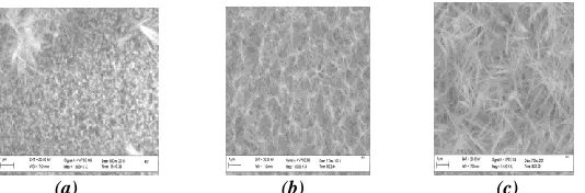
Morphological StudiesFig. 1. (a-c) show the SEM pictures of CuxO film at 100,000× magnification, deposited on glass substrate from
solutions with pH values 8, 9, 11. The films show uniform surface morphology without any pinholes and cracks. It was observed that the pH value of the solution strongly affects the obtained morphology. The copper oxide structure prepared at pH 8 is obtained in the form of compacted crystalline grains with some overgrown clusters. This overgrowth can be explained on the basis of nucleation and coalescence processes.
As the pH was increased to 9, a fiber-like nanostructure was observed and finally as the pH was increased to 11, well developed interconnected nanowires were observed there was also enhancement in the length of the fibers as well the packing density. The temperature dependence of the obtained morphology is likely due to the temperature dependence of the relative supersaturation [40]
(a) (b) (c)
Fig. 1. Scanning electron micrograph of Copper oxide thin film deposited on glass substrate (a) pH 8 (b) pH 9(c) pH 11
Figure2 (a-c) show the scanning electron micrograph of the filmdeposited on stainless steel and obtained by heating the solution bath of the anionic precursor to 70oC. The densely bundled grain nanostructures detected were spherical,
randomly oriented and does not possess porous structure. A similar structure like this one was reported by Chen (2010) [57]
The copper oxide structure obtained at pH 10, showed more concentration of the bigger snowballs at the middle of the substrate. At pH 11, the balls became smaller and more dispersed on the substrate and as the pH was increased to 12, a compacted feature of a combination of the bigger grains and smaller ones were observed.
Thus it is seen from this investigation that the type of substrate used had an effect on the morphology and grain size of the films. There was an enhancement in the grain sizes of the films deposited on stainless steel
(a) (b) (c)
http://www.gjaets.com © Global Journal of Advance Engineering Technology and Sciences 37
Compositional Analysis
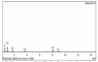
Energy dispersive X-ray analysis (EDAX) spectroscopy measurement was used to determine the quantitative analysis and stoichiometry of the as- deposited film. A typical EDAX spectrum of CuO deposited on glass substrate is as shown in fig. 3.
The EDAX analysis shows the presence of copper (Cu), oxygen (O) and the presence of other elements like Si and Ca, which are from the glass substrate.
Fig. 3. EDAX Spectrum for CuO deposited on glass substrate.
Table 1 shows the percentage weight of all the elements present in the CuO thin films deposited on glass substrate.
Table 1. Elemental composition of CuO deposited on glass substrate
Fig. 4. shows the EDAX spectrum of CuO deposited on stainless steel substrate, the analysis shows the presence of copper (Cu), and other elements like zinc (Zn) and iron (Fe) which are from the stainless steel substrate. The inclusion of oxygen could not be detected by EDAX, this indicate that pure copper was deposited.
Fig. 4. EDAX Spectrum for CuO deposited on stainless steel
Table 2 shows the elemental composition of CuO deposited on stainless steel from the table, the percentage composition of oxygen present was so minute and so in agreement with the spectrum.
pH8 pH9 pH11
Element
Weight
% Element
Weight %
Element Weight
%
C 3.46 C
2.74 C 2.6
O 31.49 O 30.9 O 33.6
Si 1.89 Si 1.16 Si 4.19
Ca 1.34 Ca 0.65 Ca 1.54
Cu 61.82 Cu 67.29 Cu 58.07
Total 100 100
http://www.gjaets.com © Global Journal of Advance Engineering Technology and Sciences 38
Table 2 Elemental composition of CuO deposited on stainless steel
pH8 pH9 pH11
Elemen t
Wei ght %
Eleme nt
Weig ht%
Elemen t
Weight %
C 1.81 C 1.94 C 1.97
O 1.86 O 1.43 O 1.85
Fe 3.39 Fe 3.94 Fe 1.64
Cu
63.3
2 Cu 67.34 Cu 43.26
Zn
30.3
2 Zn 25.45 Zn 51.28
Total 100 100 100
From the EDX spectrum and theelemental composition of CuO, it can be concluded that films deposited on glass substrate was more stoichometric than films deposited using stainless steel substrate
Structural Properties
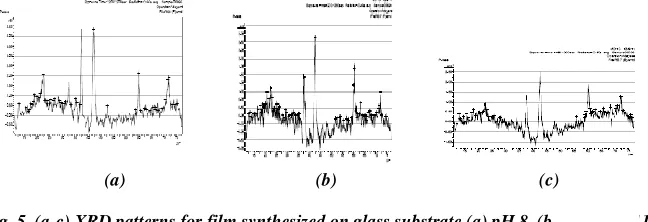
In order to confirm the formation of CuxO, and to study the crystal structures of the resultant films, XRD analyses
were employed. The effects of bath pH on the preferred orientation of SILAR deposited CuxO on glass substrates and
stainless steel substrates were investigated. The presence of multiple peaks of the CuxO phase indicates the
polycrystalline nature of films [8]. In earlier studies, CuO films obtained by ion beam sputtering and chemical vapour deposition were also reported to be polycrystalline [9].
The XRD showed that two phases, cupric oxide (CuO) and cuprous oxide (Cu2O) coexist depending on the pH of the
solution bath.
Fig. 5. (a-c) show typical XRD patterns of the thin film that were grown on glass substrate. The crystallite sizes were calculated by the X-ray line broadening method using the Scherrer formula: D = kλ / β cosθ, where λ is the wave
length of radiation used (CuKα in this case), k is the Scherrer constant (0.94), β is the full width at half maximum (FWHM) intensity of the diffraction peak for which the particle size is to be calculated, θ is the diffraction angle of the concerned diffraction peak and D is the crystallite dimension (or particle size).
All diffraction peaks reveal the formation of single phase Cu2O with cubic structure. The Miller-indexed (111), (200)
and (220), (311) reflections were the strongest which indicate that they are preferential crystal planes of the nanowire. The average crystallite size was calculated to be approximately: 0.152nm, 0.154nm and 0.167nm respectively.
(a) (b) (c)
Fig. 5. (a-c) XRD patterns for film synthesized on glass substrate (a) pH 8, (b) 9 (c) pH 11
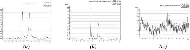
Fig. 6. (a-c) shows the XRD patterns of the thin films that were grown on stainless steel substrates for pH values 10, 11 and 12.
http://www.gjaets.com © Global Journal of Advance Engineering Technology and Sciences 39
No. 00-0003). The peaks at 2θ values of 32.74°, 37.85°, and 47.60° can be assigned to the cupric oxide crystal planes of (-110), (111), and (-202) respectively. The average crystallite size obtained for this film was 0.171nm. As the pH was increased from 10 to 11, peaks associated with cubic polycrystalline Cu2O were clearly observed (JCPDS Card
No. 05-0667). The reflections located at (1 1 1), (2 0 0), (2 2 0) and (311) planes were the strongest which indicate that they are preferential crystal planes of the nanoballs. The average crystallite size obtained was 0.144nm. As the pH was further increased from 11 to 12, the spectra showed that the synthesized oxide was copper iron oxide (CuFeO2)
(JCPDS Card No. 39-0246). The presence of Fe on the oxide indicates that there was oxidation of the stainless steel (rust). The average crystallite size obtained was 0.163nm.
There were no XRD peaks referred to Cu (OH)2, which means the grown film completely consist of only CuO
molecules, or Cu(OH)2 may be present in small extent and accumulated along the grain boundaries of the crystallites
constituting the film or Cu(OH)2 may be amorphous
(a) (b) (c )
Fig. 6 (a-c) XRD patterns of the thin film that were grown on stainless steel substrates for pH values 10, 11 and 12.
Conclusion
Successive ionic layer adsorption reaction (SILAR) method has been successfully used to synthesize and deposit polycrystalline CuO thin films on glass and stainless steel substrates. These films were characterized using X- ray diffraction (XRD), scanning electron microscopy (SEM), and EDAX. The XRD measurements showed that formation of CuO nanostructures on glass substrates are more crystalline than that are on stainless steel substrates. .
From SEM images, the grain sizes of the CuO nanostructures deposited on stainless steel were larger than films deposited on glass substrate.
Thus it is seen from this investigation that the type of substrate used had an effect on the morphology and grain size of the films. There was an enhancement in the grain sizes of the films deposited on stainless steel
Copper oxide films deposited using glass substrates showed a better morphology, higher crystallinity and better percentage ratio of the Cu/O composition than films deposited on stainless steel substrates
References
1. X. Mathew, N.R. Mathew & P.J. Sebastian, Sol. Energy Mater. Sol. Cells70 (2001), 277-286 2. A.Y. Oral, E. Mensur, M.H. Aslan & E. Basaran, Mater. Chem. Phys., 83 (2004), 140.
3. T.J. Richardson, J.L. Slack, M.D. Rubin, Proceedings of the 4th International meeting on Electrochromism,
Uppsala,( 2000)
4. G .Papadimitropoulos, N. Vourdas, V .E. Vamvakas & D. Davazoglou, Journal of Physics: Conference Series10 (2005) 182–185,
5. L. Wan, Z. Wang, Z. Yang, W. Luo, Z. Li, & Z. Zou, Journal of crystal Growth, .312, (2010) 3085–3090, 6. S.C. Ray, Sol. Energy Mater. Sol. Cells68 (2001), 307–312
7. J.F. Pierson, A. Thobor-Keck, A.Billard, Applied surface science210 (2003) 359-367
8. S. Ishizawa, T. Maruyama, K. Akimoto, Japanese Journal of Applied Physics39/2 (2000),786-788. 9. T. Murayama, Solar Energy Materials & Solar Cells 56 (1998) 85-91.
10. B. Balamurugan & B.R. Mehta, Thin Solid Films396 (2001) 90-96. 11. J.B. Forsyth, S. J. Hull, Phys.: Condens. Matter3 (1991) 5257-52 12. S. Iijima. Nature, 354 (1991) 56.
13. X. Wen, W. Zhang, S. Yang, Z.R. Dai and Z.L. Wang. Nano. Lett., 2 (2002), 1397.
http://www.gjaets.com © Global Journal of Advance Engineering Technology and Sciences 40
15. J.B. Chang, J.Z. Liu, P.X. Yan, L.F. Bai, Z.J. Yan, X.M. Yuan & Q. Yang. Mater. Lett., 60 (2006), 2125 16. J.T. Chen, F. Zhang, J. Wang, G.A. Zhang, B.B. Miao, X.Y. Fan, D. Yan and P.X. Yan. J. Alloys
Compd., 454 (2008), 268
17. Z.W. Liu & Y. Bando. Adv. Mater., 15 (2003), 303.
18. G.H. Yue, P.X. Yan, D. Yan, J.Z. Liu, D.M. Qu, Q. Yang & X.Y. Fan. J. Crystal Growth, 293 (2006), 428 19. F. Favier, E.C. Walter, M.P. Zach, T. Benter & R.M. Penner. Science, 293 (2001), 2227
20. G. H. Li, N. M. Dimitrijevic, L. Chen, T. Rajh and K. A. Gray, J. Phys. Chem. C,( 2008), 112, 19040–19044 21. Y. Liu, L. Liao, J. Li, C. Pan J. Phys. Chem. C, 111 (2007), 505
22. S. Sumikaru, S. Mori, S. Shimizu, H. Usami, E. Suzuki, J. Photochem. Photobiol. A, 194 (2008), 143 23. G.L. Luque, M.C. Rodriguez & G.A. Rivas, Talanta, 66 (2005), 467
24. H. Zhang, M. Zhang Mater. Chem. Phys., 108 (2008), 184
25. M. Singhai, V. Chhabra, P. Kang & D.O. Materials Research Bulletin, 32 (1997), 239.
26. L. Liao, Z. Zhang, B. Yan, Z. Zheng, Q.L. Bao, T. Wu, C.M. Li, Z.X. Shen, J.X. Zhang, H. Gong, J.C. Li, T. Yu Nanotechnology, 20 (2009), 08520
27. R.V. Kumar, Y. Diamant & A. Gedanken, Chemistry of Materials, 12 (2000), 2301.
28. J. Xu, K. Yu, J. Wu, D. Shang, L. Li, Y. Xu, Z. Zhu J. Phys. D: Appl. Phys., 42 (2009), 075417 29. L.B. Chen, N. Lu, C.M. Xu, H.C. Yu and T.H. Wang, Electrochimica Acta, 54 (2009), 4198. 30. J.C. Park, J. Kim, H. Kwan, H. Song, Adv. Mater., 21 (2009), 803
31. G. Ren, D. Hu, E.W.C. Cheng, M.A. Vargas-Reus, P. Reip, R.P. Allaker, Int. J. Antimicrob. Agents, 33
(2009), 587
32. D.P. Singh, Jai Singh, P.R. Mishra, R.S. Tiwari and O.N. Srivastava, Bull. Matter. Sci.31 (2008), 319–325. 33. M. Parhizkar, S. Singh, P.K. Nayak, N. Kumar, K.P. Muthe, S.K. Gupta, R.S. Srinivasa, S.S. Talwar & S.
Major, Colloids Surf. A: Physicochem. Eng. Aspects 257 (2005), 277-282.
34. F.K, Mugwang’a, P.K. Karimi, W.K. Njoroge, O. Omayio & S.M. Waita, Int. J. Thin Film Sci. Tec.2. 1, (2013) 15-24
35. M. Hari Prasad Reddy, P. Narayan Reddy and S. Uthanna, Indian J. Pure Appl. Phys.48 (2010), 420 424
36. S. Szu and C.L. Cheng, Mater. Res. Bull.43 (2008), 2687–2696
37. Y. Li, J. Liang, Z. Tao and J. Chen, Mater. Res. Bull.43 (2008), 2380–2385.
38. W. Shang, X. Shi, X. Zhang, C. Ma and C. Wang, Appl. Phys. A87 (2007), 129–135.
39. M. R. Johan, M. S. Mohd Suan, N. L. Hawari1, & H. A Ching, Int. J. Electrochem. Sci., 6 (2011)6094 – 6104
40. J S. Li, H. Zhang, Y. Ji, D. Yang Nanotechnology,15 (2004), 1428 41. S.S. Chang , Mater. Chem. Phys.,86 (2004), 247
42. S.S. Chang, H.J. Lee, H.J. Park, Ceram. Int., 31 (2005), 411
43. K. Zhang, C. Rossi, C. Tenailleau, P. Alphonse, J.Y. Chane-Ching , Nanotechnology, 18 (2007), 275607 44. R.P. Wijesundera, M. Hidaka, K. Koga, M. Sakai, W. Siripala, J.Y. Choi, N.E. Sung Phys. Status Solidi B,
244 (2007), 4629
45. G.N. Rao, Y.D. Yao, J.W. Chen, J. Appl. Phys., 105 (2009), 093901 46. A.H. Jayatissa, K. Guo, A.C. Jayasuriya, Appl. Surf. Sci., 255 (2009), 9474 47. A. Chen, G. Yang, H. Long, F. Li, Y. Li, P. Lu, thin Solid,films, 517 (2009), 4277
48. R. V. Kumar, Y. Mastai, Y. Diamant and A. Gedanken, J. Mater. Chem.,11 (2001), 1209–1213.
49. P. B. Ahirrao, S. R. Gosavi, D. R. Patil, M. S. Shinde & R. S. Patil, Archives of Applied Science Research,
3, 2 (2011), 288-291
50. Oluyamo, S.S, Nyagba, Mbafan .S, Ojo, Ambrose . S. IOSR Journal of Applied Physics 6,3 (2014), 102-105
51. J. Yang, Z. Jin, Y. Chai, H. Du, T. Liu and T. Wang, Thin Solid Films 517 (2009), 6617–6622. 52. P. Mitra, Journal of Physical Sciences, 14 (2010), 235-240
53. F. Bayansal S. Kahraman, G. Çankaya, H.A. Çetinkara, H.S. Güder and H.M. Çakmak, Journal of Alloys and Compounds, 509 (2011), 2094-209
54. L. Armelao, D. Barreca , M. Bertapelle, G. Bottaro, C. Sada, E. Tondello, Thin Solid Films 442 (2003) 48–52