IJEDR1702313
International Journal of Engineering Development and Research (www.ijedr.org)2013
Fault testing using SCOAP
Sandia controllability /observability analysis program
1
Neha Shukla,
2Karan Chandel
1P.G Scholar ,2B.tech1Electronics & Communication Engineering, 1P.E.C University of Technology, Chandigarh,India
________________________________________________________________________________________________________ Abstract—This paper describes about SCAOP for testing digital circuits. Controllability and observability of various nodes of digital circuit plays important role in testing digital circuit and detecting faults. SCOAP is a program developed by Sandia national laboratories basically deployed for testing digital circuits. This paper describes the implementation of SCOAP using an illustration of digital circuit and its drawbacks.
IndexTerms—controllability , observability ,sandia
________________________________________________________________________________________________________
I. INTRODUCTION
In any digital circuit it is very much difficult to catch that where fault exist . so many algorithms are developed for fault testing e.g, ATPG , Random test pattern generation , Sensatize-propagate and justify approach.Since there are two types of faults which are, ‘Easy to test faults’ and second one ‘Difficult to test faults’. Easy to test faults are directly analyzed by random pattern generation which identify the fault by giving random patterns at the input. But the second types of faults which are difficult to test can’t be detected through random test pattern generation .There is need of one such algorithm which must be used for testing ‘Difficult to test faults’ which is SCOAP. SCOAP is a testability measure by which it can be identified which falut is easier to test & which faults are difficult to test. It is an approximate method but it gives the approximate figure about the easier and difficult faults . by identifying them , easier faults will be removed by ‘Random Pattern Generation’ while difficult to test faults are removed by ‘Sensitize-Propagate-Justify’. This paper describes SCOAP in detail and its implementation using an example. Here there is an effort to describe the controllability, observability of a digital circuit and an attempt is made to visualize the effect of these two issues on testing the fault in a faulty digital circuit. It is based on six numerical valued analysis which are also described briefly and finally the major drawback or limitation of this analysis is identified.
II. OVERVIEW ON OBSERVABILITY & CONTROLLABILITY
Controllability
It is level of difficulty to make a net of digital circuit or we can say a signal net of any logic circuit to a particular logical value i.e, logic 0 or logic 1 with respect to primary input. It can be studied by considering figure 1.
Figure 1: Illustration of Combinational Controllability OG2
0
1 1
AND2 AND1
AND3 OG1
OG3
OG6 OG4
OG5 CC1(OG4)
CC1(OG2)
IJEDR1702313
International Journal of Engineering Development and Research (www.ijedr.org)2014
Numerical logical values involved in this analysis.
1. CC0(a):It is known as combinational 0-controllability of net ‘a’. In other words we can say that “how difficult is to make net ‘a’ of a digital circuit as ‘0’.
2. CC1(a): It is known as the combinational 1-controllabity of net ‘a’.It can also be described as ‘how difficult is to make net ‘a’ of a logic circuit as 1.
In reference to figure 1 , if there a stuck at ‘0’ fault at OG4 net then CC1(OG4) will be defined as the combinational controllability of making net OG4 as ‘1’which means ‘how difficult to make OG4 as ‘1’. Similarly CC1(OG2) is defined as combinational controllability of making OG2 as 1. The difficulty to test this fault will be defined by the add these both i.e, CC1(OG2)+CC1(OG4).
observability
1. It is also a level of difficulty which exist in propagating any digital value of signal net to the primary output. 2. C0(a): It is known as combinational obserbavility
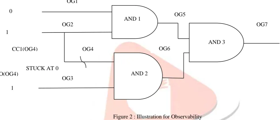
The observability of any logic value with respect to fault can be described with the help of example in figure 2.
Figure 2 : Illustration for Observability
To test the difficulty level of stuck at 0 fault of figure 2 , along with controllability , obsevability has to be considered. i.e, it should be given by CC1(OG4)+CO(OG4).
Similarly for stuck at 1 fault it will be given by CC0(l)+CO(l) where ‘l’ can be any net of any digital circuit. III. SCOAP PROCEDURE & RULES
Procedure
1. Assume the CC0 & CC1 of every primary input of the digital circuit is 1 , since some effort is required to make CC0 & CC1 as ‘1’.
2. Different SCOAP rules are defined for different logic gates , hence CC0 & CC1 are calculated as per the defined rules which are going to be discussed .
3. Similarly , the CO of every primary output is set to ‘0’ , reason being all the primary outputs are directly observable and no effort is require to observe them.
4. For different logic gates , SCOAP rules are set for obtaining observability of any logic will be discussed .
5. For calculating combinational controllability , rules must be applied from let to right i.e, from input to outpu while in case of obsevability , it has to be in opposite direction i.e, from right to left.
To propagate from left to right or from right to left some rules has to be followed .
SCOAP Rules
1. For AND gate , the combinational controllability is defined as
Figure 3 : AND gate SCOAP rule
If , it is required to make output as ‘0’ , inputs has to be zero . Thus , rule for AND gate is derived as AND 1
AND 2
AND 3 OG1
OG2
OG3
OG4
OG5
OG7
STUCK AT 0 0
1
1
OG6 CC1(OG4)
AN
CO(OG4)
OG2 OG1
0 0
IJEDR1702313
International Journal of Engineering Development and Research (www.ijedr.org)2015
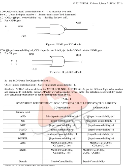
CC0(OG3)=Min{input0-controllabilities}+1; ‘1’ is added for level shift.For CC1 , both the inputs must be ‘1’ , hence submission of both is required. CC1(OG3)= ʃ{input1-controllability}+1; ‘1’ is added for level shift. 2. For NAND gate,
Figure 4: NAND gate SCOAP rule.
CC0=ʃ{input1-controllability}+1, CC1={input0-controllability}+1 is the SCOAP rule for NAND gate 3. For OR gate
Figure 5 : OR gate SCOAP rule
So , the SCOAP rule for OR gate is defined as:
CC0=ʃ{input0-controllability}+1,CC1= min{input1-controllability}+1.
Similarly , SCOAP rules are defoned for XNOR,XOR,,NOR, BUFFER etc. As per the different logic value combination and according to truth table , the SCOAP rules are well defined in form of table 1 for calculating controllability and in table 2 for calculating observability as per the assumptions taken above.
TABLE 1
SCOAP RULES FOR DIFFERENT LOGIC GATES FOR CALCULATING CONTROLLABILITY
0-Controllability 0-Observability
Primary Input 1 1
AND Min{input0-controllabilities}+1 ʃ{input1-controllability}+1 OR ʃ{input0-controllability}+1 min{input1-controllability}+1
NOT {input1-controllability}+1 {input0-controllability}+1
NAND ʃ{input1-controllability}+1 {input0-controllability}+1 NOR min{input1-controllability}+1 ʃ{input0-controllability}+1 BUFFER {input0-controllability}+1 {input1-controllability}+1
XOR Min{CC1(a)+CC0(b),
CC0(a)+CC1(b)}
Min{CC1(a)+CC0(b), CC0(a)+CC1(b)}
XNOR Min{CC1(a)+CC0(b),
CC0(a)+CC1(b)}
Min{CC1(a)+CC0(b), CC0(a)+CC1(b)}
Branch Stem0-Controllability Stem1-Controllability
Where ‘a’ & ‘b’ are nothing but the primary inputs.
In nut shell, we can say that controllability and observability of any logic circuit can be considered equivalent to the probability of occurance of logic value ‘0’ or logic value ‘1’. Out of all the possibilities the probability of ‘0’ or ‘1’ is seen under this analysis.
OG3 1
0
OG2
OG1 1
0 1
OG3
OG2 OG1
1 0 1
IJEDR1702313
International Journal of Engineering Development and Research (www.ijedr.org)2016
TABLEIISCOAP RULES FOR DIFFERENT LOGIC GATES FOR CALCULATING CONTROLLABILITY Observability
(primary , output , input ,stem)
Primary 0
AND/NAND ʃ {output obsevability,1-controllability of other inputs}+1 OR/NOR ʃ {output obsevability,0-controllability of other inputs}+1
NOT/BUFFER Output observability + 1
XOR/XNOR a : ʃ {output obsevability, min{CC0(b),CC1(b)}+1
b : ʃ {output obsevability, min{CC0(a),CC1(a)}+1
Stem Min{branch observabilities}
And finally calculation for observability is shown above .Here ‘a’ and ‘b’ are the inputs of XOR and XNOR gates.
IV. ILLUSTRATIONFORSCOAP
Figure 6 : Illustration for SCOAP. By using above equations from table 1 and table 2 we have arrived at these values.
Controllability
1. CC1(F)=CC1(A)+CC1(B)+CC1( C)+1=4 2. CC0(F)=min{CC0(A),CC0(B),CC0( C)}+1=2 3. CC1(H)=min{CC0(A),CC0(B)}+1=2
4. CC0(H)=CC1(A)+CC1(B)+1=3 5. CC1(G)=CC0( C)+1=2
6. CC0(G)=CC1( C)+1=2
7. CC1(Y)=min{CC1(F),CC1(H)}+1=3 8. CC0(Y)=CC0(F)+CC0(H)+1=6 9. CC1(Z)=min{CC0(H),CC0(G)}+1=3 10. CC0(Z)=CC1(H)+CC1(G)+1=5
Observability
1. COY(F)=CO(Y)+CCO(H)+1=5 2. COZ(G)=CO(Z)+CC1(H)+1=4 3. COY(H)=CO(Y)+CCO(F)+1=4
V. ACKNOWLEDGMENT
Working on writing in this paper was a great learning experience for us. We would like to thank God , Our Parents and Everyone who was directly or indirectly involved.
VI. CONCLUSION
From above discussion over SCOAP , it can be concluded that it is an approximate method defined for test a fault . Difficult faults are handled by complex algorithms while easier one by random pattern generation. Moreover , it can also be extended to test Sequential circuits with Flip - Flops or Registers , FSM and so on.
Z
Y
A
B
C
G1
G2
G3
G4
G5
F
H
IJEDR1702313
International Journal of Engineering Development and Research (www.ijedr.org)2017
REFERENCES[1] S. J. Piestrak, “Self-checking design in eastern europe,” IEEE Design and Test of Computers, vol. 13, pp. 16–25, 1996.
[2] S. Mitra and E. McCluskey, “Which concurrent error detection scheme to choose?,” in Proceedings of the IEEE International Test Conference, 2000, pp. 985–994.
[3] E. M. Sentovich et al., “SIS: a system for sequential circuit synthesis,” ERL MEMO. No. UCB/ERL M92/41, EECS UC Berkeley CA 94720,1992
[4] M. Geuzebroek, J. van der Linden, and A. van de Goor, “Test point insertion for compact test sets,” in Proceedings of the IEEE International Test Conference, 2000, pp. 292–301.
[5] M. Gossel and S. Graf, Error Detection Circuits, McGraw-Hill, 1993
[6] Naeimi H and DeHon A, “Fault-tolerant nano-memory with fault secure encoder and decoder,” presented at the Int. Conf. NanoNetw., Catania, Sicily, Italy, Sep. 2007.
[7] L.H Goldstien “Analysis of Multiple Faults in Synchronous Sequential Circuits by Boolean Difference Techniques”, Private Communication [8] C. T. Ku and G. M Mason, “The Boolean Differ ence and Multiple Fault Analysis”, ZEEE Trans. on Computers, Vol. C-21, No.1 Jan 1975,
pp.62-71
[9] NPTEL video course by Prof . Jatindra Kumar Deka , Dr. Santosh Biswas , IIT Guwahati.
NEHA SHUKLA