INTERNATIONAL JOURNAL OF ENGINEERING SCIENCES & MANAGEMENT
165
I
NTERNATIONAL
J
OURNAL OF
E
NGINEERING
S
CIENCES &
M
ANAGEMENT
IMPLEMENTATION OF LINEAR CURRENT MODULATION FOR LED DRIVER IC
Anju Kuhar*¹, Himanshi Saini² [M.Tech Scholar*, A.P]
ECE -VLSI Design, Deenbandhu Chhotu Ram University of Science and Technology
,Murthal
ABSTRACT
The Light-Emitting Diode (LED) driver is an important part of Visible Light Communication (VLC) systems. The main challenge of the VLC LED driver is to offer a high data transmission rate with high power efficiency. This paper presents the design, analysis and layout of a white light LED driver that combines the LED lighting with VLC technology and their different level of signal analysis. This paper presents three approaches that is device modeling, reduction of leakage current and design of Silicon on insulator (SOI).The proposed LED driver uses linear current regulation and controls the AC current signal and the DC current through a single power device for the purposes of high speed, high efficiency and high integration. In addition, this work presents an impedance reduction technique to enhance the bandwidth of the LED driver. And a first-order pre-equalizer is utilized to enhance the electron-optical-electron (E/O/E) bandwidth in the VLC system due to the bandwidth limitation of the phosphor converted LED. So, LED driver adds the VLC technology into solid-state lighting successfully.
I.
INTRODUCTION
Linear current modulation
As shown in Fig. 1, for the purpose of an accurate driven current ILED, the driver is under close-loop control, which is generated by connecting the control IC to the power MOSFET M1 and the current sense resistor R1. By the way, VCS is the driver’s output voltage and the driving current is equal to VCS /R1. Because of the linearly first-order relationship of ILED and VCS, the driver with linear current modulation has been achieved. Furthermore, the linear driving circuit also realizes the purpose of controlling the DC and AC signal through a single power device M1. The control IC’s output voltage VCS is equal to DC signal plus data signal. In other words, the LED’s driving current ILED involves the command of lighting and Communication. So the LED driver adds the VLC technology into solid-state lighting successfully.
Fig.1 Comparison of two architectures [20]
A small-signal model of the LED can be seen as a voltage control current source, which is used to control the LED’s DC and AC current with linear modulation method.
Stage of power device
INTERNATIONAL JOURNAL OF ENGINEERING SCIENCES & MANAGEMENT
166
is to decrease the equivalent capacitance at the gate of the power MOSFET. There are two LED drivers, which are both consisted of the white light LED (MX-3) of Cree Corporation and n-MOSFET (Si3456DDV) of Vishay Corporation.
As shown in the left side, the driver’s electric bandwidth is limited by this large equivalent capacitance. To solve the problem comes from the large equivalent capacitance due to the output impedance of power MOSFET’s drain is increased by the number of LEDs; the right side driver discloses the impedance reduction technique. Hence, the driver’s equivalent capacitance at the gate of the power MOSFET can be decreased and its bandwidth can be extended as well. In brief, this work utilizes the impedance reduction technique to achieve a large bandwidth, high driving current, and high efficiency driver.
Control IC design
The control IC’s output voltage VCS is equal to DC signal plus data signal. It is for the purpose of combining the DC current for lighting with AC current for data transmission through a single power device. The control IC of the driver not only can provide a large driving current but also a high speed data transmission with its wide bandwidth. The function blocks of the driver are which are error amplifier, voltage adder, voltage regulator and bias circuit.
Error Amplifier:For the purpose of high gain, high driving capability and high linearity, the error amplifier of the control IC is realized by a folded cascade amplifier with class AB output stage. [18], because the feedback voltage on the current sense resistor is reference to ground and in the low voltage range, the p-MOSFET differential input is suitable for the folded cascade amplifier. The entire gain of error amplifier is equal to the gain A1 of folded cascade amplifier multiplied by the gain A2 of class AB output stage. The feedback loop of the error amplifier is compensated by the cascade miller compensation, and its small-signal analysis Compare with general miller compensation, the no dominant pole in is higher than that in the general miller Compensation. Furthermore, the compensation capacitor is connected to low impedance at its left side, which will make the total harmonic distortion of the error amplifier better.
Voltage Adder: The purpose of the voltage adder is to combine the DC lighting signal VLD with AC signal VIS for data transmission, and to provide the proper signal to the error amplifier after it., the voltage VX is equal to (VLD + VIS)/2 because the two resistances at the input nodes, VLD and VIS, are the same. And the output voltage Vmix will be equal to (VLD + VIS)/2 after the signal VX is amplified by the non-invert amplifier A1. By the way, if the value of is 1, the Vmix will be equal to VLD + VIS.
Pre-equalizer
Even through the electric bandwidth of LED driver is achieved with impedance reduction technique, the optical bandwidth is limited by the phosphor-converted LED which needs a long response time to convert an electric signal to a light signal. In order to solve this problem, the pre-equalizer is presented to compensate this bandwidth limit due to the phosphor-converted LED. [12] The pre-equalizer is the first-order architecture, which is constructed of R1, C1 and R2.
II.
PRESENTED WORK
The presented work is described by a flow chart as shown in fig.2.
Semiconductor device modeling
INTERNATIONAL JOURNAL OF ENGINEERING SCIENCES & MANAGEMENT
167
LEVEL 1 model is most often used to simulate large digital circuits in situations where detailed analog models are not needed. LEVEL 1 models offer low simulation time and a relatively high level of accuracy for timing calculations. If you need more precision (such as for analog data acquisition circuitry), use the more detailed models, such as the LEVEL 6 IDS model or one of the BSIM models (LEVEL 13, 28, 39, 47, 49, 53, 54, 57, 59, and 60). For precision modeling of integrated circuits, the BSIM models consider the variation of model parameters as a function of sensitivity of the geometric parameters. The BSIM models also reference a MOS charge conservation model for precision modeling of MOS capacitor effects.
Reduction of leakage current in mosfet
INTERNATIONAL JOURNAL OF ENGINEERING SCIENCES & MANAGEMENT
168
Fig. 3 Leakage current difference between a single off device and a stack of two off devices. [4]
Proposed SOI mosfet design
The basic idea underlying silicon-on-insulator technology is to remedy this by electrically insulating the thin layer at the wafer surface carrying the electronic devices from the bulk wafer used as mechanical support. This can be achieved either through placing the device layer onto a wafer made from an insulating material or, in a sand- which structure, through separating the device layer from the silicon bulk with an insulating interlayer as shown in fig. (Fig. 4) [1]. Most current SOI approaches focus on the sandwich structure [1, 2]. Fabricating devices in the thin device layer of an SOI substrate a variety of advantages, many of which result from the reduction or elimination of unwanted parasitic interactions between the devices and the bulk substrate [1].
Fig.4 SOI Design Preparation.[5]
Fundamental of SOI:
Silicon on insulator (SOI) technology refers to the use of a layered silicon–insulator–silicon substrate in place of conventional silicon substrates in semiconductor manufacturing, especially microelectronics, to reduce parasitic device capacitance, thereby improving performance. SOI-based devices differ from conventional silicon-built devices in that the silicon junction is above an electrical insulator, typically silicon dioxide or sapphire (these types of devices are called silicon on sapphire, or SOS). The choice of insulator depends largely on intended application, with sapphire being used for high-performance radio frequency (RF) and radiation-sensitive applications, and silicon dioxide for diminished short channel effects in microelectronics devices. The insulating layer and topmost silicon layer also vary widely with application.
Need to SOI design:
INTERNATIONAL JOURNAL OF ENGINEERING SCIENCES & MANAGEMENT
169
Higher performance at equivalent VDD. Can work at low VDD's.
Reduced temperature dependency due to no doping and also reduced antenna issues. Better yield due to high density, better wafer utilization. So, no body or well taps are needed. Lower leakage currents due to isolation thus higher power efficiency.
Inherently radiation hardened (resistant to soft errors), thus reducing the need for redundancy.
FINFET
Of the listed solutions, the Fin FET presents itself as a good candidate to extend the lifetime of the field-effect transistor – a near-term solution to the problems facing the IC industry. Its manufacturing is not trivial, and changes in circuit design methodology seem daunting. Yet, the Fin FET is a structure that has already been researched for nearly 15 years, and is the most readily-integrated of the “non-classical CMOS” devices. In addition to transistors that are based on field-effect principles, researchers have studied more ambitious, long-term solutions to today’s scaling issues. Structures such as resonant tunneling devices have applications in both logic and memory circuitry, with their first application as a complement of the FET, rather than its replacement, and are considered for near-future implementation, but a riskier and currently costlier proposition than some non-classical FETs. At the same time, devices based on single-electron operation, molecular transistors, or spin transistors are all considered far-future solutions [2] that may or may not pan out, carrying with them the highest amount of risk, and most often, complete abandonment of legacy concepts of design and manufacture of integrated circuits. The multiple research efforts in the Fin FET arena have already produced impressive results from both academia and industry. However, Fin FETs are not the only solution to the problems of continued scaling. The first and most obvious approach is to continue with traditional planar CMOS technologies until a fundamental barrier, such as the size of the silicon atom, is achieved. The costs associated with transition to entirely new types of devices are immensely prohibitive, considering the time and investment needed to establish new design and manufacturing processes.
III.
SCHEMATICS AND SIMULATION
Fig.5 First-order equalizer.
Fig.6 Small-signal analysis of miller compensation.
+
V G1R1 1k C1 1u R2 1k V1 5 + VG1 2.5 VF1 C 1 4 7 n V2 5 VF2 C 3 4 7 n R1 50 R2 100k C2 1n
-++ U1 OPA340
INTERNATIONAL JOURNAL OF ENGINEERING SCIENCES & MANAGEMENT
170
Gain Vs Frequency Graph
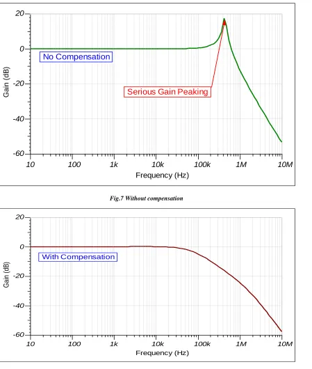
Fig.7 Without compensation
Fig .8 With compensation.
T
Serious Gain Peaking
Frequency (Hz)
10
100
1k
10k
100k
1M
10M
G
a
in
(
d
B
)
-60
-40
-20
0
20
No Compensation
Serious Gain Peaking
T
Frequency (Hz)
10 100 1k 10k 100k 1M 10M
G
ai
n
(d
B
)
-60 -40 -20 0 20
INTERNATIONAL JOURNAL OF ENGINEERING SCIENCES & MANAGEMENT
171
Fig.9 Comparison between Equalizer and without equalizer output.
Fig.10 Analog to digital converter for LED operating.
AVDD
GND GND
AVDD
V1 5
Out:1
C
1
2
0
0
p
R
2
2
k
sclk:2
din:3
sync:4
DAC5311
SYNC SCLK DIN
A
V
D
D
G
N
D
OUT
U2 DAC5311
SCLK SDO SYNC
INTERNATIONAL JOURNAL OF ENGINEERING SCIENCES & MANAGEMENT
172
Fig.11 Differential amplifier
Fig.12 LED Driver circuit.
INTERNATIONAL JOURNAL OF ENGINEERING SCIENCES & MANAGEMENT
173
Fig.13 Output waveform
Fig.14 Differential amplifier layout.
T
Time (s)
0.00 15.00 30.00
VF1
0.00 4.95
VF2
0.00 4.94
VF3
0.00 4.93
VF4
0.00 4.87
INTERNATIONAL JOURNAL OF ENGINEERING SCIENCES & MANAGEMENT
174
Fig.15 LED Driver layout
INTERNATIONAL JOURNAL OF ENGINEERING SCIENCES & MANAGEMENT
175
Fig.16 Parameter value and output trace of LEVEL 1
LEVEL 1 MODEL:
The Level 1 MOSFET model should be used when accuracy is less important than simulation turn-around time. For digital switching circuits, especially when only a “qualitative” simulation of timing and function is needed, Level 1 runtime can be about half that of a simulation using the Level 2 model. The agreement in timing is approximately 10%. The Level 1 model, however, results in severe inaccuracies in DC transfer functions of TTL-compatible input buffers, if these buffers are present in the circuit. The channel-length modulation parameter LAMBDA is equivalent to the inverse of the early voltage for the bipolar transistor. LAMBDA is a measure of the output conductance in saturation. When this parameter is specified, the MOSFET has a finite but constant output conductance in saturation. If LAMBDA is not input, the Level 1 model assumes zero output conductance.
INTERNATIONAL JOURNAL OF ENGINEERING SCIENCES & MANAGEMENT
176
Fig.17 Trace of signal for LEVEL 3 analysis
3. BSIM (BERKELEY SHORT-CHANNEL IGFET MODEL): (W=3, L=1Micrometer)
INTERNATIONAL JOURNAL OF ENGINEERING SCIENCES & MANAGEMENT
177
Fig.18 Graph of BSIM Model
Different colored line shows voltage and red line show average voltage.
IV.
CONCULUSION
The LED driver in this paper combines the function of lighting with VLC technology. The LED driver uses linear current regulation and controls the AC and DC current signal through a single power device for the purposes of high speed, high efficiency and high integration. In addition, this work utilizes an impedance reduction technique to enhance the electric bandwidth of it. And a first-order pre-equalizer before control IC is utilized to enhance the E/O/E bandwidth which is limited by the phosphor-converted LED original. This VLC LED driver is fabricated in a standard 0.5µm CMOS technology with chip area 154µm×1250µm. It is available in a standard SOP-16 pin package. The LED driver circuit is in CMOS process and exhibits a worst-case power consumption100mW with 33mA peak PWM current . The future scope is the technique that accomplish both leakage reduction and process sensitivity reduction such as combining MTCMOS sleep transistor technique for leakage reduction and the current biasing scheme. LED driver all circuit design layout in nano scale [FINFET]. FIN FET circuit provide stability of all LED driver IC and low fluctuation and low leakage current that provide higher gain and high speed circuit design.
REFERENCES
1. MAHENDER VESHALA, “CMOS Digital Integrated Circuit Analysis and Design”, page-208, 3rd Edition, Tata McGraw Hill publication 2011.
2. MAKARA TANG, “CMOS VLSI Design: A Circuit and System Perspective”, 4th Edition,
3. “RONALD D. SCHRIMPF,” Modern VLSI Design, 3rd Edition (I.P. Based Design) 4th Edition prentice hall publication 2008
4. JUN MA, “Application -Specific Integrated Circuits (ASICs)”, IJETE, Volume 1 Issue 2, pp- 40-44, March 2014.
5. SIVA G. NARENDRA, Divakar Shahi, Sh. Nishant Tripathi, “Design of 1.2Volt, 1GSPS, 2, 3, 4And 6 Bit Flash ADC Using EIS Comparator and Fat Tree Encoder”, IJAERT, Volume 2 Issue 6, pp- 206-210, September 2014.
6. G.SRINIVASULU, “Design of8 Bit ALU Using Microwind 3.1”, IJAERT, Volume 2 Issue 2, pp- 50-55, May 2014.
7. ELHAM KHAYAT MOGHADDAM, “Design of Charge Shared Power Optimized Pulse Triggered Flip Flop”, IJETE, Volume 1 Issue 10, November 2014
INTERNATIONAL JOURNAL OF ENGINEERING SCIENCES & MANAGEMENT
178
9. SUMIT SINGH, Parikha Chawla, “Design & Analysis of High Speed Low and Area CMOS based Comparator with Different Architectures”, IJETE, Volume 1 Issue 7, August 2014
10. TRIPATI SUBUDHI, Rajesh Mehra, “Design Analysis of CMOS Voltage Mode SRAM Cell using Different nm Technologies”, IJETE, Volume 1 Issue 3, April 2014
11. RUPALI S. BALPANDE and Rashmi S. Keote., “Design of FPGA based Instruction Fetch & Decode Module of 32-bit RISC (MIPS) Processor, International Conference on Communication Systems and Network Technologies 2011.
12. H. LI, X. CHEN, B. HUANG, and D. TANG, “High Bandwidth Visible Light Communications Based on a Post-Equalization Circuit,“ IEEE Photonics Technology Letters., vol. 26, pp.119-122, Jan.2014.
13. “ANALOG INTEGRATED CIRCUIT DESIGN’’ by tony chanand david A. johnesbin second edition. 14. H. LE-MINH, D. O’BRIEN, G. FAULKNER and L. ZENG, “High-Speed Visible Light Communications
Using Multiple-Resonant Equalization,“ IEEE Photon. Technol. Lett., vol. 20, pp.1243-1245, July.2008.sss 15. H. LE-MINH, D. O’BRIEN, G. FAULKNER and L. ZENG, “100-Mb/s NRZ Visible Light Communications
Using a Postequalized White LED,“ IEEE Photon. Technol. Lett., vol. 21, pp.1063-1065, Aug.2009. 16. C. W. CHOW, C. H. YEH, Y. F. LIU and Y. LIU, “Improved modulation speed of the LED visible light
communication system integrated to the main electricity network,“ Electron. Lett., vol. 47, pp.867-868, July.2011.
17. H. LE-MINH, D. O’BRIEN, G. FAULKNER and L. ZENG, “80 Mbit/s Visible Light Communications using pre-equalized white LED,“ Proc. ECOC, 2008, pp.1-2.
18. R. HOGERVORST and J. H. HUIJSING, “ Design of Low-Voltage, Low-Power Operational Amplifier Cells”, Kluwer Academic Publishers, 1996.
19. IMRE KNAUSZ. (2004) [online]. Available: www.knausz.com/files/opamp_final_paper2.pdf.
![Fig.4 SOI Design Preparation.[5]](https://thumb-us.123doks.com/thumbv2/123dok_us/8354292.1668141/4.612.84.493.80.235/fig-soi-design-preparation.webp)