Abstract— A novel fast locking digital phase-locked loop (DPLL) has been proposed with simple control unit to improve locking time. A frequency difference stage (FDS) is added to produce a 3-bit code represents the difference between the input frequency and the output frequency of the PLL. This code is used to control a programmable charge pump (PCP) output current. As the difference between the two frequencies decreases, the PCP output current decreases to obtain smooth PLL locking. As locking is achieved, the PCP operates with its conventional current. The proposed DPLL is designed using 130nm CMOS process with a 1.2V power supply. It operates in the frequency range 250MHz – 1.75GHz. Over this frequency range, a locking time reduction in the range of 35.7% - 66.6% has been achieved compared with conventional DPLL.
Index Term— Fast locking, Phase locked loop, Frequency difference stage, Programmable charge pump.
I. INTRODUCTION
Phase-Locked Loop (PLL) is one of the most important synchronizing circuits used in transceivers, communication systems, etc. Conventional digital PLL (DPLL) should be modified to achieve fast locking. Different techniques have been used to obtain fast locking DPLLs [1-7]. In this paper, a novel DPLL is proposed to achieve fast locking by varying the PLL bandwidth. Wide bandwidth is used when the PLL is in the out-of-lock state, while the narrow bandwidth is used when the PLL is in the lock state. This can be accomplished by applying additional current to the conventional charge pump current in the out- of- lock state.
Mohamed A. Ahmed. Author is with the Electronics Research Institute (ERI). National research center, physics buildings- ElBohous st, Dokki, Giza, Egypt :
Heba A. Shawkey Author is with the Electronics Research Institute (ERI).
Hamed A. Elsemary Author is with the Electronics Research Institute (ERI).
Abdelhalim A. Zekry Author is with the Faculty of engineering, Ain Shams university.
The additional current is provided by a programmable charge pump (PCP); its output current depends on the output code from the frequency difference stage (FDS). This code represents the difference between the input frequency and the output frequency. As this difference decreases, the code from the FDS decreases and the PCP output current decreases to obtain smooth transition to lock. As locking is achieved, the conventional current of the PCP is used to provide loop stability [4]. The paper is organized as follows: section II explains the operation of the proposed DPLL. Section III describes the design for each block of the proposed DPLL. Section IV presents complete simulation performance for each block. Finally, section V shows the conclusions.
II. OPERATION OF THE PROPOSED DPLL
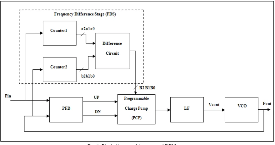
Fig. 1 shows the block diagram of the proposed DPLL. The FDS and the PCP-instead of the conventional CP-are added to achieve fast locking. The FDS consists of two frequency counters and a difference circuit. Each counter is used to count its input frequency during a fixed period and produces a 3-bit code proportional to the input frequency. The 3-bit code from each counter is fed to the difference circuit which produces a 3-bit code (B2 B1 B0) represents the difference between the two counter codes. The 3-bit code from the difference circuit is used to control the PCP output current. During lock state, counter1 and counter2 produce the same 3-bit code, so B2 B1 B0 is zeros, and the PCP operates at its conventional current. When the input frequency changes, counter1 produces a different 3-bit code, B2 B1 B0 becomes non-zero code, and the PCP outputs a current proportional to the difference between the input and the output frequencies. As this difference decreases, the PCP output current decreases until it reaches the conventional current and hence a smooth transition to lock is obtained. The gradually switching from the PCP highest current to the PCP conventional current improves the proposed DPLL stability.
Mohamed A. Ahmed, Heba A. Shawkey, Hamed A. Elsemary , Abdelhalim A. Zekry
A Fast Locking Digital Phase-Locked Loop
Fig. 1. Block diagram of the proposed DPLL.
III. DESIGN OF THE PROPOSED DPLL
In the following sections, different building blocks of the proposed DPLL are introduced.
A. Frequency Difference Stage (FDS)
The purpose of the FDS, shown by the dashed line in Fig. 1, is to produce a 3-bit code represents the difference between the input and the output frequencies. It consists of two frequency counters (counter1 and counter2) and a difference circuit. Counter1 counts the input frequency and produces a 3-bit code (a2 a1 a0) represents the counted frequency. Counter2 counts the output frequency and produces a 3-bit code (b2 b1 b0) represents the counted frequency. Each counter code is applied to the difference circuit which produces a 3-bit code (B2 B1 B0) represents the difference between them. In the following sections, we introduce in details one of the two frequency counters and the difference circuit.
i. Frequency counter
Fig. 2 shows the block diagram of the 3-bit frequency counter. The input frequency and the time-window signal (a clock signal with 4ns pulse width) are applied to an AND logic gate to count the number of input frequency pulses in the 4ns. The choice of the 4ns is to cover the frequency range of 250MHz – 1.75GHz as shown in Table I. The ring counter is used to produce 7-bit code corresponding to the number of frequency pulses that coming in the 4ns. The 7-bit code is converted to a 3-bit code using an encoder circuit. Each bit of the 3-bit code from the encoder is applied to the D input of a positive edge triggered D flip flop. The time-window signal is inverted through an inverter and applied to the clock input of each D flip flop. As the time-window signal becomes low, all the three D flip flops are triggered and output the 3-bit code
(counting result) to the difference circuit. This code is being used until the time- window signal becomes low again. So, the 3-bit code from the counter is updated every 8ns. To count the frequency all the time, we can use two frequency counters in each counter block. Fig. 3 shows the implementation of counter1 using two frequency counters, the code from which is updated every 4 ns (time-window pulse width).
Fig. 2. Block diagram of the frequency counter.
TABLEI
CONTROL BITS RELATED TO THE FREQUENCY.
No. of cycles in the 4ns time window
0
Frequency
<250MHz
B2 B1 B0
000 1
2
250MHz 001
500MHz 010
3 750MHz 011
3 5 6 7 or more 1GHz 100
1.25GHz 101
1.5GHz 110
Fig. 3. Block diagram of Counter1 using two frequency counters.
Ring counter
Fig. 4 shows the implementation of the 8-bit ring counter used in the frequency counter. It uses positive edge triggered D flip flops with active low Set/Reset inputs [8]. The time-window signal input which forces the ring counter to zero is connected to the R input of all the flip flops and to the S input of FF0. When the time-window signal goes low, all the flip flops are reset except FF0 which is set. Thus, when the ring counter is reset, its content is 10000000. The input frequency is applied to the clock input of all the flip flops. On the rising edge of the first clock pulse (input frequency), FF0 having 0 on its D input resets, while FF1 having 1on its D input sets, and the bits shift one place to the right and the count becomes 01000000. On the second clock pulse similarly 00100000 is counted and so on. To maintain D7 equal 1 when 7 pulses or more are coming during the time-window is high, we remove the feedback from D7 to D0 and connect D0 to ground, and we apply D0, D1, D2, D3, D4, D5, and D6 to a 7 input NOR gate which produces 1 on its output only when all its inputs are 0, this happens only when the output of FF7 is 1. The output of the 7 input NOR gate and the output of FF7 are applied to an OR gate, the output of which is considered as D7.
Fig. 4. Block diagram of the ring counter.
Encoder
The encoder is used to convert the 8-bit from the ring counter into a 3-bit applied to the difference circuit. The truth table of the encoder is shown in Table II.
TABLEII ENCODER TRUTH TABLE.
D7D6D5D4D3D2D1D0 0000000 0000001 0000010 0000100 0001000 0010000 0100000 1000000
a2a1a0 000 001 010 011 100 101 110 111
From Table II, we can write:
a0=D1+D3+D5+D7 (1) a1=D2+D3+D6+D7 (2) a2=D4+D5+D6+D7 (3) By using (1), (2), and (3), we can implement the encoder circuit as shown in Fig. 5.
Fig. 5. Encoder circuit diagram.
ii. Difference circuit
The difference circuit receives counter1 output code (a2 a1 a0) and counter2 output code (b2 b1 b0) and produces a 3-bit code (B2 B1 B0) represents the difference between the two counters codes. It is simply a subtract circuit. The output of the difference circuit is applied to the PCP to control its output current. The implementation of the difference circuit is based on the subtraction process using twos-complement method. The following example illustrates the performing steps if the minuend is greater than the subtrahend [8].
Minuend = 101 stays unchanged 1 0 1 Subtrahend = 010 take twos-complement 1 1 0 Discard end carry 0 1 1 The following example illustrates the performing steps if the minuend is less than the subtrahend [8].
Minuend = 010 stays unchanged 0 1 0 Subtrahend = 101 take twos-complement 0 1 1 No end carry 1 0 1
Take the two's-complement of the sum 101 0 1 1
another twos-complement process is performed. Fig. 6 shows the implementation of the difference circuit using the sequence illustrated in the above two examples. Counter1 output code (a2 a1 a0) is considered as the minuend, while counter2 output code (b2 b1 b0) is considered as the subtrahend. Each bit of the minuend is directly applied to a full adder (FA), while each bit of the subtrahend is inverted and applied to a full adder. To complete the twos-complement process, we connect the third input of FA0 with the power supply rail, VDD. To perform the twos-complement process on the sum S2 S1 S0, each bit is inverted and applied to a half adder (HA) and the second input of HA0 is connected to VDD. The end carry is applied to the select input of the three 2*1 Muxs. If there is an end carry, the minuend is greater than the subtrahend, take the outputs S2 S1 S0. If there is no end carry, the minuend is less than the subtrahend, take the outputs R2 R1 R0. Another way to implement the difference circuit is to compare the two codes, if a2 a1 a0 > b2 b1 b0, the code a2 a1 a0 is considered as the minuend while the code b2 b1 b0 is considered as the subtrahend. And if b2 b1 b0 >= a2 a1 a0, the code b2 b1 b0 is considered as the minuend while the code a2 a1 a0 is considered as the subtrahend. The logic implementation of the compare circuit is shown in Fig. 7.
Fig. 8 shows the implementation of the difference circuit using compare circuit. The output of the compare circuit is applied to the selection input of Mux1, Mux3, and Mux5, while the inverted of the output of the comparator circuit is applied to the selection input of Mux2, Mux4, and Mux6. If a2 a1 a0 > b2 b1 b0, the output of the compare circuit is high, so, each bit of the code a2 a1 a0 is applied directly to a full adder, while each bit of the code b2 b1 b0 is applied to a full adder through an inverter. If b2 b1 b0 >= a2 a1 a0, the output of the compare circuit is low, so, each bit of the code b2 b1 b0 is applied directly to a full adder, while each bit of the code a2 a1 a0 is applied to a full adder through an inverter.
Fig. 7. Compare circuit logic diagram.
B. Phase Frequency Detector (PFD)
Fig. 9 shows the schematic of the PFD used in the proposed DPLL. It compares the input frequency Fin with the PLL output frequency Fout and gives two output signals (UP and DN) depending on the frequency and phase difference between them [9].
C. Programmable Charge Pump (PCP)
Fig. 10 shows the circuit of the PCP [10], it outputs eight current levels by using the three additional current mirrors M0, M1, and M2 controlled by the three MOS switches S0, S1, and S2 respectively. The 3-bit control code B0, B1, and Fig. 6. Difference circuit logic diagram
Fig. 9. PFD schematic.
B2 from the difference circuit is applied to the three MOS switches S0, S1, and S2, respectively, to control the three current paths and to determine the output current level. The UP signal from the PFD is applied to PMOS P0 through an inverter and the DN signal is directly applied to NMOS N0. When B0=0, B1=0, and B2=0, the PCP operates with its conventional current level (IREF). When B0=1, B1=1, and B2=1, the PCP operates with the highest current level. The UP and DN signals controls the direction of the output current, while the 3-bit control code controls the level of the output current as shown in Table III.
Fig. 10. The programmable charge pump circuit.
TABLE III
PROGRAMMABLE CP OUTPUT CURRENT Output current (mA) B2B1B0
0.1 000
0.337 001
0.553 010
0.7 011
0.974 100
1.1 101
1.2 110
1.36 111
D. Loop Filter
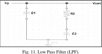
A passive loop filter is used to convert the output current from the charge pump into a control voltage (Vcont) input to the VCO [11]. The second order passive loop filter shown in Fig. 11 is used in the proposed DPLL with C1=10pF, C2=52pF, and R2=368ohm.
Fig. 11. Low Pass Filter (LPF).
E. Voltage Controlled Oscillator (VCO)
The 5-stage current starved VCO [7] shown in Fig. 12 is used in the proposed DPLL. The VCO is designed to operate linearly in the range of 250MHz – 1.75GHz. The VCO output frequency is shown in Fig. 13.
Fig. 12. Schematic of the 5-stage Current-Starved VCO.
Fig. 13. VCO output frequency.
IV. SIMULATION RESULTS
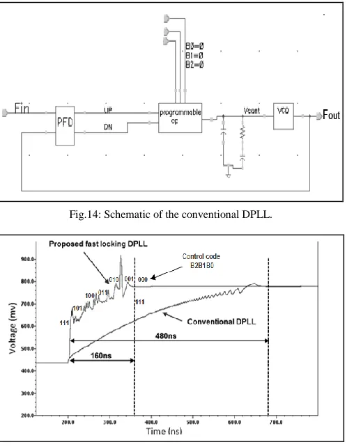
Fig.14: Schematic of the conventional DPLL.
Fig. 15. Simulation of the conventional DPLL and the proposed DPLL.
TABLEIV
LOCK TIME COMPARISON FOR PROPOSED AND CONVENTIONAL PLL
Frequency Change
(GHz)
Conventional DPLL (ns)
Proposed DPLL
(ns)
Reduction (%)
0.25 -1.7 480 160 66.6
0.25 -1.5 340 120 64.7
0.5 -1.3 210 90 59
1.7 -0.25 220 100 54.5
0.6 -1.2 150 80 46.6
.5 -1 140 80 42.8
1.3-0.5 140 90 35.7
TABLEV
SUMMARY OF THE PROPOSED DPLL PERFORMANCE.
Reference [2] [5] [7] This work
Technology 0.35𝜇m CMOS
65nmCMOS 0.18𝜇m CMOS
0.13𝜇m CMOS
Freq. range (MHz)
358-1440 400-1600 200-2000 250-1750
Freq. change (MHz)
880 800 300-800 600-1200
Lock time 3𝜇s 52𝜇s 0.092𝜇s 0.08𝜇s supply voltage
(V)
3.3 1.1 3.3 1.2
Power consumption
(W)
0.0231 N/A N/A 0.075
V. CONCLUSIONS
A novel DPLL is designed to operate in the frequency range of 250MHz – 1.75GHz and achieve fast locking. The fast locking is achieved by adding a frequency difference stage (FDS) to produce a 3-bit code represents the difference between the input and the output frequencies. The 3-bit code from the FDS is used to control the PCP output current. As the frequency difference between input frequency and output frequency decreases, the PCP output current decreases until reaches its conventional value at locking. Simulation results show that for the frequency changes in the range of 250MHz - 1.75GHz, the lock time reduction is in the range of 35.7% - 66.6% compared with the conventional DPLL.
REFERENCES
[1] Wagdy, M. F., Sur, R., 2012, April. A Novel SAR Fast-Locking Digital PLL: SPICE Modeling and Simulations. In: International Conference on Information Technology: New Generations, Las Vegas, Nevada, 472-477.
[2] Cheng, K.-H., Yang W.-B., Ying, C.-M., 2003, November. A Dual-Slope Phase Frequency Detector and Charge Pump Architecture to Achieve Fast Locking of Phase-Lock Loop. IEEE trans. analog and digital signal processing, vol. 50, no. 11.
[3] Sadeghi, V. S., Naimi, H. M., Kennedy, M. P., 2012. A fast charge pump PLL using a bang-bang frequency comparator with dead zone. In: IEEE International Symposium on Circuits and Systems (ISCAS), 1379 - 1382.
[4] McDonald, J. J., Hulfachor, R. B., 2005,. Circuitry to Reduce PLL Lock Acquisition Time. U. S. Patent # 6,940,356, 6.
[5] Amourah, M. , Krishnegowda, S., Whately, M., 2013. A Novel OTA-Based Fast Lock PLL. In: IEEE Custom Integrated Circuits Conference (CICC), 1-4.
[6] Assaf, B.-B., Haifa, 2009, September. PLL Lock Time Reduction. U. S. Patent #7,595,698, Sep. 2009.
[7] Wagdy, M. F., Cabrales, B. C., 2009. A Novel Flash Fast-Locking Digital Phase-Locked Loop. In: Sixth International Conference on Information Technology.
[8] Karris, S. T., Digital Circuit Analysis and Design with Simulink Modeling and Introduction to CPLDs and FPGAs, Orchard Publications, Second Edition.
[9] Ali, M., Elsemary, H., Shawkey, H., Zekry, A., 2010. A fast locking digital phase-locked loop using programmable charge pump. In: IEEE International Conference on Computer Engineering and Systems,135– 138.
[10] Alvarez, J., Sanchez, H., 1994. charge pump with a programmable pump current and system. U. S. Patent #5,362,990.
[11] Keese, W. O., 1996, May. An Analysis and Performance Evaluation of a Passive Filter Design Technique for Charge Pump Phase-Locked Loops. National Semiconductor, Inc., Application Note 1001, http://www.national.com.