A Gate Diffused Input Based CMOS Full Adder
Circuit for Low Power, High Speed Applications
Yamini Verma Shivangini
M. Tech Student M. Tech Student
Department of Electronics and Communication Engineering Department of Electronics and Communication Engineering Indira Gandhi Delhi Technical University for Women,
Kashmere Gate, Delhi, India
Indira Gandhi Delhi Technical University for Women, Kashmere Gate, Delhi, India
Prof. Ashwani Kumar Professor
Department of Electronics and Communication Engineering Indira Gandhi Delhi Technical University for Women, Kashmere Gate, Delhi, India
Abstract
As the technology is shrinking down we are required not only to reduce device size area but also reduce power dissipation, energy consumption and delay. Here adder circuit is the main component which is mostly used in computations that require for many applications in microprocessors. So here in this paper, our main purpose is to reduce power and delay in the CMOS adder circuit. So we have introduced a new design technique known as GDI (Gate Diffused Input) technique. GDI based full adder circuit is compared with power gating adder circuit. In power gating method, sleep transistor is used and also decreased the width, length ratio. In modified design, GDI XNOR based adder is used but it gives better results analysis than the base design. Proposed design gives the less number of transistors, low power, low energy consumption and less delay over the conventional method. Simulation has been done in the 90 nm TSMC Technology using Cadence Virtuoso tool.
Keywords: adder, CMOS logic, GDI, Power gating, XNOR
________________________________________________________________________________________________________
I. INTRODUCTION
In VLSI applications, for arithmetic operations mostly adder is used so in other words, we can say that adder is the heart of VLSI design system. Thus the adder is the basic building block of the system so the performance of adder in VLSI system applications affects directly. Here recently in past few years, low power applications demand has been increased due to the MOS scaling factor. In scaling phenomena as the chip size is decreasing but complexity in the chip is increasing, so power dissipation is increasing thus to maintain or control the power is our main challenge of design.
In this paper, we have designed 1-bit full adder using XOR/XNOR gates. Recently, full adder has been designed by researchers in different logic styles as the pseudo-NMOS adder, TG (Transmission Gate) adder, PTL (Pass Transistor Logic) adder for improving performance. We have proposed a new design of full adder based on GDI. In digital circuits, our main concern is energy efficiency, delay, power delay product parameters. Digital circuit operates in the sub-threshold mode for achieving low power. In weak inversion region, when the gate to source voltage is less than the threshold voltage then ideally current assumes zero but practically small sub-threshold leakage current flows in transistor. This sub-threshold current flows due to the minority carriers in the channel. So if supply voltage is less than the threshold voltage so it produces a sub-threshold current that is the main reason for reducing power dissipation in the circuit. By reducing power and area of chip that can be reduced by using a small number of transistors, we can achieve low delay or high operating speed for the design. The product of the small amount of delay and power defines the minimal PDP (Power Delay Product). As we know that energy efficiency depends upon power so we can also obtain low energy and this is advantageous for achieving power and energy efficient designs.
II. CONVENTIONAL FULL ADDER DESIGN
A Gate Diffused Input Based CMOS Full Adder Circuit for Low Power, High Speed Applications (IJSTE/ Volume 3 / Issue 12 / 029)
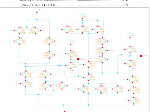
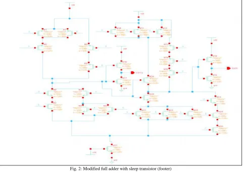
In 1-bit full adder designing, we used 90 nm UMC technology so we considered minimum width as 120 nm and 100 nm as length. The W/L ratio of Conventional CMOS full adder 3.1 times that of NMOS in Design (where NMOS is fixed at 1.2 and W/L of PMOS is 3.8) which is shown in the Fig.1 and after modified in base design we put W/L ratio of PMOS is 1.5 times that of W/L ratio of NMOS ratio. Each block sizing ratio is based on assumptions only and each block assumes as an equivalent inverter. In design 1 we added sleep transistor in the footer. After that, we compared the conventional adder design with reduced width/length ratio sleep transistor based full adder design and we obtained results with some reduction in power and delay shown in Fig.3. Full adder designed by truth table and Boolean expressions for outputs are defined as follows:
Sum= (𝑎bc)………..……….. (1)
Cout=(ab)c + (aʘb)a………...(2)
Fig. 2: Modified full adder with sleep transistor (footer)
A Gate Diffused Input Based CMOS Full Adder Circuit for Low Power, High Speed Applications (IJSTE/ Volume 3 / Issue 12 / 029)
III. PROPOSED FULL ADDER
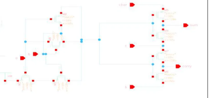
GDI technique has an advantage that it can reduce large complex function into less no. of functions. Gate diffused input is a novel design technique use for low power digital circuit. GDI cell contains three inputs that are G (common state input of NMOS and PMOS), P (input to the source or drain of PMOS) and N (input to the source or drain of NMOS). In this, the source of PMOS is not connected to VDD and source of NMOS is not connected to ground that is the difference from normal MOS transistor. Here basic GDI cell is shown below –
Fig. 4: Basic GDI cell
Various logic gates can be implemented using GDI cell. We have shown below some modification of logic functions based on GDI –
Table - 1
Various logic functions based on GDI
So with the help of GDI cell, we have designed 1-bit full adder using XNOR function. a, b, c are taken as bit input for one-bit full adder. Sum and carry are generated by using inputs. GDI full adder needed only 8 transistors for design thus no. of transistors from base design to modified design has been reduced from 29 transistors to 8 transistors only.
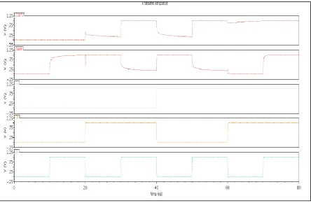
Fig. 5: Transient analysis of GDI based adder
Schematic diagram of full adder based on GDI is shown in figure no. 4 and corresponding waveform shown below in figure no. 5. Proposed design has not only improved power, delay but also reduced size. Energy dissipation has been also reduced.
IV. SIMULATION RESULT
In this paper, all the circuits have been designed on the base of CMOS logic and simulations have been done on cadence virtuoso using 90 nm technology. Power supply voltage is given 1V in each case and all comparison is done on the basis of simulation results. Power consumption has been greatly reduced from base design to modified design. All the parameters power, delay, PDP, area have been examined and compared with base design 1 and design 2. All simulation results are given as below-
Table - 2
Simulation result comparison
Parameter Design 1 Design 2 Modified Design
Technology (nm) 90 90 90
Supply voltage (v) 1 1 1
Power (nѡ) 133.50 75.38 2.674 Delay (ps) 119.90 104.80 25.86 PDP (aws) 16.01 7.89 0.069
Transistors count 28 29 8
V. CONCLUSION
After comparing the simulation results we get the reduction in power dissipation, propagation delay in GDI full adder design. Here power has been reduced 43.5% in design 2 and 98% in modified design in comparison to base design 1. The propagation delay has been improved 12.59% in design 2 and 78.43% in modified design in comparison to base design 1. Power delay product that is PDP is also reduced 50.71% in design 2 and 95.69% in modified design. Thus in GDI full adder complexity has been reduced over conventional designs and the comparison between our designs and prior works indicates that one of our designs does provide its advantages. In short, the proposed designs can be taken a better alternative.
REFERENCES
[1] Mayank Sharma, Sandip Nemade,Vikas Gupta, “Optimal Design for Ground Bounce Noise Reduction Using Sleep Transistor,” International Journal of Engineering Innovation & Research, vol. 2, no. 5, Sept. 2013
[2] K.Navi, O. Kavehei, M. Rouholamini, A. Sahafi, S. Mehrabi, N. Dadkhai, “Low-Power and High-Performance 1-bit CMOS FullAdder Cell,” Journal of Computers, Academy Press, vol. 3, no. 2,Feb. 2008.
A Gate Diffused Input Based CMOS Full Adder Circuit for Low Power, High Speed Applications (IJSTE/ Volume 3 / Issue 12 / 029)
[4] Pren R. Zimmermann, W. Fichtner, “Low-power logic styles: CMOS versus pass-transistor logic,” IEEE J. Solid- State Circuits, vol. 32, pp. 1079–1090, July 1997.
[5] A. Bazzazi And B.Eskafi, “Design And Implementation Of Full Adder Cell With Gdi Technique Based On 0.18um Cmos Technology”, volume 2, 2009 [6] K.Bernstein et al., “Design and CAD challenges in sub-90nm CMOS technologies,” in Proc. int. conf. comput. Aided Des., 2003, pp.129-136.
[7] “International Technology Roadmap for Semiconductors,” Semiconductor Industry Association, 2005. [Online]. Available: http://public.itrs.net
[8] H.Felder and J.Ganger,”Full Chip Analysis of Leakage Power Under Process variations, Including Spatial Correlations, “in proc. DAC, pp.523-528, June2005. [9] Jun Cheol Park and Vincent J. Mooney” Sleepy Stack Leakage Reduction” IEEE transactions on very large scale integration (vlsi) systems, vol.14, no.1.
november 2006.
[10] Harmander Singh, Kanak Agarwal, Dennis Sylvester, Kevin J. Nowka,”Enhanced Leakage Reduction Techniques Using Intermediate Strength Power Gating,”IEEE Transactions on VLSI Systems,Vol.15, No.11, November 2007.