Implementation and Performance Evaluation of
FIFO Buffer Design of NOC Routers
Shilpa Kodgire1, Dr. U. D. Shiurkar2
1Ph.D. Research Scholar NIELIT Aurangabad, 2Director, DIEMS Aurangabad
Abstract: In this paper we present power dissipation and delay is the predominant factor in the buffer design of NoC router. We propose an improved buffer design called FIFO buffer. Designed buffer has chip area and power dissipation minimum while delay is no greater than a upper bound. Buffer has been designed in VLSI and control logic is designed by FSM with significant improvement in a chip area and power consumption is achieved. The proposed buffer has been designed and simulated in Active HDL and Synopsys tool 90 nm and 45 nm technology. End results shows improvement in area, latency and throughput. Keywords: NoC, VLSI, FIFO,HDL,FSM
I. INTRODUCTION
A FIFO buffer is a useful way of storing data in NoC routers asynchronously but cannot be read immediately. A FIFO buffer stores data on a first-in, first-out basis. The storage structure is typically an array of contiguous memory. Data is written to the “head” of the buffer and read from the “tail”. When the head or tail reaches the end of the memory array, it wraps around to the beginning. If the tail runs in to the head, the buffer is empty. But if the head runs in to the tail, the implementation must define if the oldest data is discarded or the write does not complete.
Buffering is required in most on-chip routers to provide temporary storage of packets that are in transit, and also to control traffic of transmitting data. Buffering is implemented mostly with first-in, first-out (FIFO) memory and can be expensive in terms of area for on-chip application [1]. It is better to transmit packet instead of storing them because more power consume in storing them as compared to transmission. Thus reduction in number and size of buffer increase system performance and reduces area and power consumption. Buffer size and the buffering scheme are the two main considerations [2].
There are various buffering schemes, namely input buffering, output buffering and shared buffering [3]. Advantages and disadvantages for each buffering, is discuss below.
With output buffering, mean queue length of systems is always found to be shorter than the mean queue length of an equivalent system with input buffering. This is because with output buffers, switching are performed before buffering, hence inputs are isolated from output congestion up to the point that a target output has no remaining buffer capacity [3]. Shared buffering shares a set of buffers between multiple input and output ports. It is costly to implement because of the associated control overhead. In concept of shared buffering, buffering places within the crossbar switch to provide smaller designs and superior performance than output buffering [3] While in Input buffering structure is simple, internal link speed of the multistage interconnection network is same as the input and output port (4)This document is a template. For questions on paper guidelines, please contact us via e-mail.
II. PROPOSEDMETHODOLOGY
In proposed architecture, data transfers by segmenting longer messages into smaller data packets, and forwarding these packets individually from sender to the receiver possibly with different routes and delays for each packet. Packet switching offers the potential for scalability. Packets are composed of fields as shown in Fig.1, each field carrying specific information. FIFO is designed in a bottleneck i.e. one less location than the number of ports. For five port router four location FIFO is designed. The width of the FIFO is equal to the size of the packet. Here packet size is of 40 bits. The first part is the header that contains three bit source address. Second part is destination address of three bit and remaining bits indicate payload portion in which user specify its contents. Packetization of data allow to use wide interconnects for on-chip networks, thus increases the performance.
HEADER PAYLOAD Fig.1 Packet Format
In proposed router buffering is required to provide temporary storage of packets that are in transit. There is one input channel at each port, each running its own finite state machine (FSM) control logic. Each input channel has a first in first out (FIFO) buffer of depth 4 and data width of 40 bits and a control Logic which has been implemented as a FSM.The FIFO FSM controller has role of receiving a forty bit packet from the output port of the adjacent router and stores them in FIFO buffer and manages the flow control between adjacent routers. The input channel accepts request from other neighbouring router. On receiving the request, if it is free, it will acknowledge the request. Input channel will accept packet as long as the request signal is held high. The previous router's output channel ensures that the request line is held high until it completely transmits the packet to input channel. Complete transmission of packet occurs if and only if FIFO buffer of that input channel is not full and width of the buffer storage and the on-chip interconnect equal to the packet size. Thereby avoiding the need to transfer a packet in segments. In this manner, the requirement for full packet reception is easily met with reduced complexity. The input channel sets the acknowledge line high, as long as there is a transfer taking place. The packet of data received from the previous router is stored locally in the FIFO buffer thereby implementing a store-and-forward data flow. When the transfer of packet is completed, the request and acknowledge lines go low in sequence.
III.IMPLEMENTATION
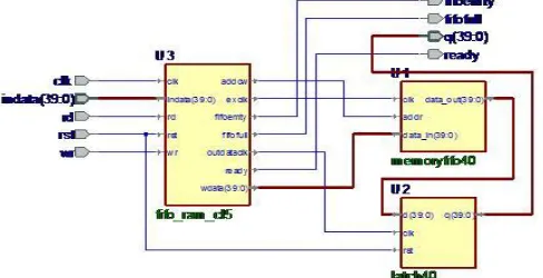
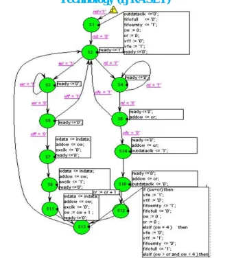
Fig 2 shows, implemented block diagram of first in first out (FIFO) buffer and fig 3 its control logic. FIFO buffer consist of FIFO control logic that control read and write operation of that corresponding input port. Reset and clock signal is connected to FIFO buffer.
When read signal (rd) or write signal (wr) to that input port is high then FIFO control logic performed read or write operation respectively for that port only. Fig 3 shows FSM description of control logic. Read counter (cr) and write counter (cw) are the variables which stores number of read and write operation performed on that FIFO buffer. These variables are used to know whether the FIFO is empty or full. During read or write operation ready signal is low indicating, that particular channel is currently busy. When read signal is high (rd=1), control logic first check fifoempty signal. If fifoempty signal is high it means FIFO is empty and no more data is available to performed read operation and operation is terminated. If fifoempty signal is low it means there is some data residing in FIFO memory, so packet is read from memory and read counter (cr) is incremented by one.
[image:3.612.191.435.583.708.2]When write signal is high (wr=1), control logic first check fifofull signal. If fifofull signal is high, it means memory is full and noore packets are added in it and operation is terminated. If fifofull signal is low, it mean FIFO memory is not full there is some space to store new arriving packet, so newly receiving packet can be write into the memory. The address of memory location where the packet is be to store is also generated by FIFO control logic and write counter(cw) is incremented by one. After these operations read counter (cr) and write counter (cw) are compared. If read counter (cr) is equal to write counter (cw), it means number of read operation performed is equal to number of write operation, so signal is updated accordingly given as below. Condition of read counter is checked, if write counter is equal to read counter then fifoempty (fe) signal becomes high which indicate that FIFO buffer is now become empty and fifofull (ff) signal becomes zero. If write counter is equal to four (cw=4), it means only write operation is performed four times, since buffer memory depth is of four places therefore after these four write operation buffer became full. So signal is updated accordingly explain as below. Condition of write counter is checked if it is equal to four then fifoempty (fe) signal became low and fifofull (ff) signal became high indicate that buffer is full. Similarly, if write counter (cw) is bigger than read counter and less than maximum storage locations, it means buffer is not completely empty, some data residing inside that nor buffer is full, so fifoempty signal and fifofull signal became zero.
Fig. 3 Control Logic of First in First Out Buffer
IV.RESULTANDCONCLUSION
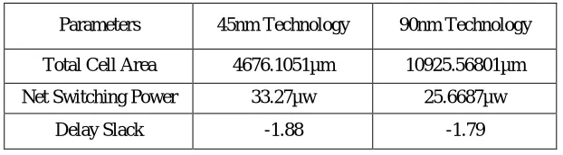
Synchronous FIFO Buffer is implemented, design and Simulation is done on ActiveHDL9.3. The result of the simulation is as in fig 4
[image:4.612.64.565.508.707.2]TABLE I.
PARAMETER COMPARISION IN SYNOPSYS
V. CONCLUSION
The NoC router’s buffers are major consumers of area and power, and responsible for its performance. Moreover, buffers are used to facilitate enhancing performance and allowing deadlock freedom. In this paper, a novel low latency and low power router buffer architecture are compared with two different technology, while achieving the good performance compared to the much more expensive, traditional routers FIFOs. FIFO buffers can be used as virtual channels to avoid deadlock problem. Thus it increases throughput of existing NOC designs.
In this paper a novel FIFO buffer architecture, for packet size of 40 bit, address capacity of 8 port, and depth of 4 memory level design are presented. FIFO buffer design first tested in ActiveHDL9.3 tool for simulation and verification of design. After that we evaluate its area, power and other parameters using Synopsys tool. The result of area and power come in micro scale range. FIFO design is an interface between external world and arbiter, so we tried our best to keep minimum pin for the interface which also reduces the wiring complexity and further outcomes.
REFERENCES
[1] B. Attia, W.Chouchene, A. Zitouni,N. Abid and R. Tourki, “A Modular Router Architecture design for Network on Chip,” 8th International Multi conference
on Systems, Signals and Devices,-2011
[2] M. Sood and V. Tiwari, “Performance Evaluation of Network on Chip Router Architecture by using VHDL,” vol no 2 pages 154-158, Jan-2011
[3] S. S. Mehra, R. Kalsen and R. Sharma, “ FPGA based Network-on-Chip Designing Aspects,” National conference on Advanced Computing and
Communication Technology, ACCT-10
[4] S. A. Asghari, H. Pedram, M. Khademi and P. Yaghini, “Designing and Implementation of a Network on Chip Router Based on Handshaking Communication
Mechanism,” World Applied Sciences Journal 6(1):88-93, 2009
[5] C. A. Nicopoulos D. Park, J. Kim, N. Vijaykrishanan, M. S. Yousif, and C. R.Das, “ViChaR: A dynamic virtual channel regulator for network-on-chip routers”
in MICRO39: Proceddings of the 39th Annual IEEE/ACM International Symposium on Microarchitecture, Dec-2006, pp 333-346
[6] M. Mitic, and M. Stojcev, “An Overview of On-Chip Busses”, Facta Universitatis (Nis) Ser: Elec. Energ, vol 19, No.3, Dec-2006, pp. 405-428.
[7] S. A. Asghari, H. Pedram, M. Khademi and P. Yagihini, “Designing and Implementation of a Network on Chip Router based on handshaking Communication
Mechanism”, World Applied Sciences Journal 6(1): 88-93, 2009
Parameters 45nm Technology 90nm Technology
Total Cell Area 4676.1051µm 10925.56801µm
Net Switching Power 33.27µw 25.6687µw