International Journal of Emerging Technology and Advanced Engineering
Website: www.ijetae.com (ISSN 2250-2459, ISO 9001:2008 Certified Journal, Volume 7, Issue 7, July 2017)
258
Accelerating Thyroid Imaging Studies using Blackfin Pipelined
Vision Processor
Murali Ravi
1, Siva Sankara Sai S
2 1,2Sri Sathya Sai Institute of Higher LearningAbstract — The computational resources of a System on Chip (SoC) accompanied by their compact design tailors to the needs of current medical devices where there is a necessity for visualizing and performing diagnosis in real-time. Currently we are developing a Small Organ Imaging Gamma Camera (SOIGC) for imaging small organs with higher spatial and energy resolution. We present here a novel ”SoC” based real-time medical image processing tool for evaluation and quantification of Thyroid Uptake Ratio derived from Single Photon Emission Computed Tomography (SPECT). The Thyroid Uptake Ratio is a diagnostic index used extensively to assess Thyroid’s hormonal activity obtained by quantifying the intensity of the segmented SPECT images which are conventionally done on expensive propriety tools. In contrast to these, our lower cost SoC tool based on DSP architecture offers a higher speed image segmentation process with co-relating performance. Thus, it also eliminates the need for higher computing resources on the host machine by using a Hardware accelerator called ”Pipeline Vision Processor” of an optimized Dual Core Digital Signal Processor. This architecture offers a high performance enhanced infrastructure with large on-chip memory and reduces the overall bandwidth requirement leading to accelerated imaging.
We have validated the performance of this tool by evaluating it on a case with thyroid medical history. As compared to diagnosis by propriety SIEMENS software or segmentation tools based on MATLAB, our hardware accelerated approach has shown a drastic reduction of computational time of about 250% with superior correlation.
Keywords—System on Chip (SoC), Digital Signal Processing (DSP), Pipelined Vision Processor (PVP), Medical Imaging.
I. INTRODUCTION
Imaging algorithms require innovative architecture solutions to increase the efficiency of the operation.
A lot of energy is consumed in solutions depending exclusively on Instruction Level Processors (ILPs). On the contrary the ASIC type of Instruction Programming approach fares very well with respect to performance and power efficiency but does not allow the kind of flexibility and software environment the ILPs offer. Hence, there is a need for a combination of both of the above advantages [1]. Implementing most image processing algorithms on the host PC has several disadvantages due to the computational load it induces on the system. A lot of serial operations have to be implemented to configure a single step of computation. This makes the option of real-time imaging a challenging task as the algorithm conflicts with the programs running on the host PC, demanding its portion of resources like memory, bandwidth, pipelining tasks, resources sharing [2]. Computationally demanding functions like masked spatial filter, image segmentation and Integral Image Computation are more demanding on the resources of the host PC.
International Journal of Emerging Technology and Advanced Engineering
Website: www.ijetae.com (ISSN 2250-2459, ISO 9001:2008 Certified Journal, Volume 7, Issue 7, July 2017)
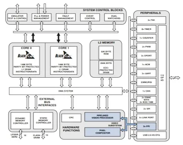
[image:2.612.118.488.131.424.2]259
Figure 1. Architecture of BF609 Chip
Typically for a thyroid scan, this acquisition goes on for about 12 minutes which leads to large amount of data generation. In our research group, effort towards minimizing the time taken to run the Image Reconstruction and Processing algorithms is attempted. The idea is to use the power of hardware acceleration to execute the algorithms which is considered computationally costly due to the load it induces on the host PC. In this paper, the work completed in hardware acceleration of Image Processing is presented. We also report the comparative performance of the same algorithm on three different platforms. The speed and accuracy of the analysis has also been compared.
II. ANALOG DEVICES DSPBF609
A Digital Signal Processor, is a microprocessor that is optimized for the operative needs of digital signal processing. DSP can process real time data, making it suitable for applications that are intolerant to delays. Digital signal processors take digital signals and process them to improve the signal to produce either clear sound, faster data or sharper images.
A unique processor from Analog Devices with Blackfin architecture called BF609 is being used to achieve hardware acceleration of Image processing.
The ADSP-BF609 processor is a member of the Blackfin family of products. Blackfin processors has the advantages of a RISC-like microprocessor instruction set, and single instruction, multiple-data (SIMD) with a dual-MAC signal processing engine which can process multimedia capabilities into a single instruction-set. ADSP-BF609 Blackfin processors are a new type of embedded processors designed to meet the computational demands of today’s imaging systems where performance and power constraints exists [3] [4].
International Journal of Emerging Technology and Advanced Engineering
Website: www.ijetae.com (ISSN 2250-2459, ISO 9001:2008 Certified Journal, Volume 7, Issue 7, July 2017)
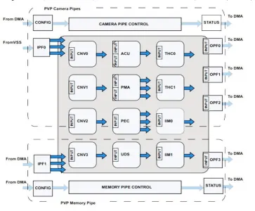
[image:3.612.128.491.128.428.2]260
Figure 2. Pipeline Vision Processor
In addition to these, the ADSP-BF609 processor contains features for safety-critical applications, including a Cyclic Redundancy Check for memory protection, Parity and ECC protection in the internal memory blocks [5].
Each processor core consists of two 16 bit multipliers, 40 bit shifter, two 40 bit accumulators, two 40 bit general purpose ALUs and four 8 bit Video purpose ALU. Single MAC can perform a 16-by-16 multiplications in one cycle and ALU operation on 16 bit or 32 bit data.
Blackfin processor supports a modified Harvard Architecture with a categorized memory structure. All the resources that include I/O control registers, Memory (Internal and External) occupies separate sections in this unified address space. These memory portions are arranged hierarchically for maintaining good performance balance between cache memories of fast and low latencies along with lower cost, larger off chip memories. For example, L1 memory is a fast and low latency cache memory which typically operates at the full processor speed, while, off chip memory systems are SDRAM, flash memory and SRAM which can be accessed using External Bus Interface Unit (EBIU).
Memory DMA controller handles the block transferring of code or data between internal and external memory spaces providing high bandwidth data movement capability.
III. ADVANTAGES OF PVP
Pipelined Vision Processor provides a set of 12 high performance signal processing blocks that can be combined to form data processing pipes. These blocks are optimized for tasks typical of video and image processing, robotics, and 2-dimensional vector applications. The PVP works in tandem with processor cores. It is optimized for convolution and wavelet based object detection, classification, tracking and verification algorithms. PVP offers more than 25 giga operations per second (GOPs) with very low memory bandwidth and configurable datapaths. PVP operates on frame rates up to 1280x960x30Hz (16bits).
International Journal of Emerging Technology and Advanced Engineering
Website: www.ijetae.com (ISSN 2250-2459, ISO 9001:2008 Certified Journal, Volume 7, Issue 7, July 2017)
261
The Block diagram of PVP is shown in Figure 2. The definitions of each block that a PVP houses is given below [6]:
Cartesian to Polar Magnitude and Polar Angle conversion (PMA): This is used when conversion of two 16- bit signed inputs in Cartesian format (x,y) into Polar form (Magnitude, Angle) is required. Identification of non-zero pixel crossing in edge detection algorithms can be done with PMA.
Convolution (CNV): This block supports 2D convolution of pixel ranges - 1x1, 3x3, 5x5 and upto 16 bit coefficients. The PVP has four such convolution blocks. Calculation of the first and second derivatives of pixel ranges and Gaussian image smoothening can be done using the CNV block coefficients.
Integral Image Computation: Integral image blocks calculates a 2-Dimensional integral over the input frame and outputs the summed area table (SAT). Alternatively, these blocks can generate a rotated SAT (RSAT) or can integrate in horizontal dimension only (integral row mode).
Pixel Edge Classification Block: PEC supports edge detection including: non-linear edge enhancement filtering in a pixel neighborhood, edge classification based on orientation, subpixel position interpolation, vertical/horizontal sub-pixel position into one byte per pixel. PEC operates either in first derivative mode (PEC-1) or second derivative mode (PEC-2).
Threshold-Histogram-Compression Block: The statistical and range reduction signal processing functions are implemented by the threshold-histogram-compression. Many other PVP blocks can be connected to this block using the PVP’s pipeline interconnection options.
Up-Down Scaling Block: The up-down scaling block expects a 16-bit or 32-bit unsigned input data and drives 32bit output data. When an anti-aliasing or an averaging filter is enabled, the input must be 16 bits and correspondingly the output is 16 bits presented in the lower 16 bits of 32-bit output.
Output Formatters (OPFn): OPFs collect data results of PVP blocks, apply final formatting, and forward the results to the DMA channels. The OPF0, OPF1, OPF2 serves the camera pipes. The PF3 serves the memory pipe. Each OPF is associated with a specific DMA channel.
Input Formatters (IPFn): IPFs can recieve data directly from the video input interface (the Enhanced Parallel Peripheral Interface (EPPI)) and from memory through DMA.
[image:4.612.329.549.288.502.2]IPFs incorporate pre-processing including color or luminance components extraction, pixel windowing, frame counting, and control the frame processing. The camera pipe and memory pipes are the two architectures supported by the PVP at the same time. The processor interaction is not required for inputting the pixels from the camera interface as it can be dine directly. This completely eliminates the overhead of reading pixels from the system interface. A complete application can be built only out of the functional blocks of the PVP as we can have direct access to the I/O interfaces. The BF609 can perform upto 25 billion operations per second in four concurrent applications and yet consume as less as 80 mW [5].
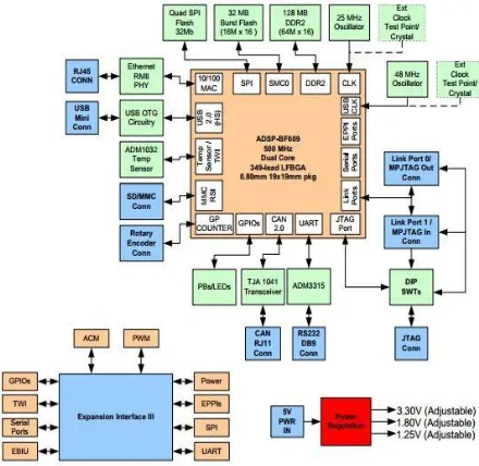
Figure 3. Block Diagram of BF609 EZ Kit
IV. MATERIALS USED
This section lists all the software and hardware tools, processor boards used to accomplish this task of hardware accelerated image processing. Lab set-up for evaluation is shown in Appendix.
A. ADSP BF609 EZ Kit board
International Journal of Emerging Technology and Advanced Engineering
Website: www.ijetae.com (ISSN 2250-2459, ISO 9001:2008 Certified Journal, Volume 7, Issue 7, July 2017)
262
B. Stand Alone Debugging Agent (SADA)
An Interface for a processor with PC is required to facilitate the execution of DSP algorithms as well as to visualize the results. An In Circuit Emulator (ICE) or a stand-alone debugging agent (SADA) is used to interface the PC to Joint Test Action Group (JTAG) header on the processor. The Standalone Debug Agent provides a modular low cost emulation solution for EZ-Boards.
C.Cross Core Embedded Studio (CCES)
Cross Core Embedded Studio is a integrated development environment (IDE) for the Analog Devices Blackfin and SHARC processor families. It is an Eclipse based IDE and employs the latest generation of mature code generations tools which provides seamless, intuitive C/C++ and assembly language editing, code-gen, and debug support. The IDE includes driver support for on chip and off chip peripherals, stacks for Ethernet and USB, a popular real time operating system and file system. It provides an easy to use development framework for working with BF609.
V. METHODS
A. Configuring the BF609
[image:5.612.326.565.325.671.2]This section deals with detailed analysis of the methods deployed for the medical image segmentation using the BF609 processor. This is a application with an entry point of commands at Core0 from the CCES. Figure 4 shows how t application is distributed inside the processor.
Figure 4. Developed control flow in BF609
Core 0 takes in image frames from the host PC in the form of text file and the segmented image from the Region of Interest is handed over to PVP. The multi-core library manages all the signaling and buffer exchanges between cores.
Transfers of data between peripheral and memory or between two memories are done by DMA channels. These channels can transfer data between off-chip and on-chip memories. DMA manages all the memory related access.
DMAxx CFG register configures the specific allotted DMA channel and can be done using the option:
Pvp_mempipeInputDMAConfig()
The following code snippet shows the configuration of the 43rd channel of the DMA which serves as PVP0 Memory Pipe Data Input.
void Pvp_mempipe_InputDMAConfig()
{
*pREG_DMA43_ADDRSTART = nBuffer; ssync();
*pREG_DMA43_XCNT = 128u * 128u; ssync(); *pREG_DMA43_XMOD = 4u; ssync();
[image:5.612.52.285.481.694.2]*pREG_DMA43_CFG= NUM_DMA_CFG_ADDR1D
|ENUM_DMA_CFG _STOP
|ENUM_DMA_CFG _MSIZE04
|ENUM_DMA_CFG _PSIZE04
|ENUM_DMA_CFG _SYNC
|ENUM_DMA_CFG _READ
|ENUM_DMA_CFG _EN
ssync();}
International Journal of Emerging Technology and Advanced Engineering
Website: www.ijetae.com (ISSN 2250-2459, ISO 9001:2008 Certified Journal, Volume 7, Issue 7, July 2017)
263
In the input section, the IPF register PVP_IPFn_CTL controls the IPFn pipeline features that include color format, Unpack Incoming, output port selection and format conversion. PVP_IPFn_HCNT and PVP_IPFn_VCNT contains horizontal and vertical counts (Pixels) for the region of interest at PVP_IPFO_VPOS and HPOS respectively.
Each block of the PVP can be configured to specify the block from which the input is received and the block to which the input is further sent. The registers have to be carefully manipulated so that the right setting is configured. The following code snippet shows the configuration of the IIM block inside the PVP whose configuration structure as shown in Figure 5.
*pREG_PVP0_IIM1_CFG =
(ENUM_PVP_IPF1<<
BITP_PVP_CNV_CFG_IBLOCK0
[image:6.612.329.561.137.247.2]| (0 << BITP_PVP_CNV_CFG_IPORT0) | (BITM_PVP_OPF3_CFG_MPIPE)
| BITM_PVP_IIM_CFG_START;
*pREG_PVP0_IIM1_CTL = (ENUM_PVP_IIM_CTL_RECTMODE)
|(ENUM_PVP_IIM_CTL_SINGLE32);
Each configuration register can be manually configured by looking into its structure and locating the specific bits. The above code configures the IIM whose structure is as given below:
Similarly all the blocks of the PVP have to be configured and the signal flow as shown in Figure 4 is developed. This flow establishes the path the image takes in the processor while the segmentation and the data extraction is performed. Once the coordinates of the portion of the image to be segmented is set by the user, the PVP is configured to count the pixel intensities in the ROI as the pixel intensities reveal the spatial distribution of the isotope in the patient body. The functioning of the IIM in PVP is similar to set of ray sum along the region specified by the user. The Figure 6 summarizes the function of IIM.
Figure 6. Functioning of IIM block
B. Thyroid Segmentation using BF609
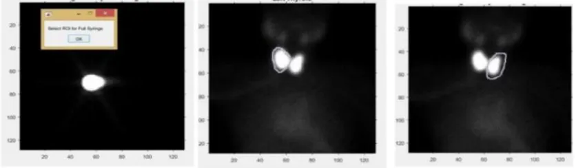
In a typical thyroid study, the radiopharmaceutical is introduced into the patient intravenously. The isotope is allowed to distribute around the body. The tracer presence around the other parts of the body contribute to the background of the region which has to be manually subtracted. The thyroid study receives background counts by the accumulation of the tracer in nearby salivary glands, mediastinum organs.
The thyroid imaging follows a four step imaging process. Initially, the full dosage in the syringe is imaged to estimate the total number of counts. The syringe is again imaged after the tracer is injected into the body as a part of it gets left behind in the syringe. A part of the tracer also accumulates near the site of injection, this is called as antecubital. The difference of total count and the above two would give an estimate of the amount of tracer which entered into the body. The following formula calculates the Thyroid Uptake Ratio:
* 100
Standard CPM = (Full syringe counts) - (Empty syringe + Antecubital counts)
CPM = Counts per minute.
International Journal of Emerging Technology and Advanced Engineering
Website: www.ijetae.com (ISSN 2250-2459, ISO 9001:2008 Certified Journal, Volume 7, Issue 7, July 2017)
264
A. Approach 1: Host PC based Segmentation:
To calculate the time it would take to run the same file on Host PC, ROI based segmentation algorithm was written in MATLAB. The program was run on a 2.2 GHz, 64 bit, Intel i7, 8GB RAM with 6MB cache. Functions like
imfreehand() were used to draw ROI extract the pixel intensities. The time taken for the computation was generated using MATLAB’s internal timer and displayed using profiler.
B. Approach 2: ADSP BF609 SoC based Segmentation:
The EZ kit containing the BF609 was connected to a Intel i5, 64 bit, 8GB RAM computer using the SADA daughter card. This chip is used as a bridge to interface the BF609’s JTAG using the USB. The code was dumped into the chip using the CCES. The relevant inputs and outputs were accessed by performing file I/O operations. The time taken to run the algorithm was timed by a digital timer.
VI. RESULTS AND DISCUSSION
The anonymized patient’s thyroid images were taken and were run on all of the three platforms to check the performance with respect to its computational efficiency and the time it takes to complete these tasks. The SoC based segmentation performed as efficiently as the SIEMENS software tool for the patient data. The results are shown in Table 1.
[image:7.612.325.561.148.214.2]The SoC based segmentation showed 96% accuracy in terms of the index prediction but showed 100% accuracy in terms of the disease prediction. The reason for 4% error can be attributed to the way in which the ROI selection was done, which is an acceptable margin. In terms of time, the chip consumed about 250% less time for segmentation, pixel extraction and computation of the index parameters compared to the time it took to run the same algorithm in the Host PC. This shows that SoC design reduces the time taken to complete the algorithm.
TABLE I:
Comparison between approaches
Thyroid Uptake Ratio (%) Time in seconds (s)
HOST PC SOC HOST PC SOC
15.6 14.98 49 20
Acknowledgements
The authors wish to thank Analog Devices Inc. for supplying us with the BF609 EZ Kit and for their continued support. We wish to thank our Founder Chancellor Sri Sathya Sai Baba and the University for providing us infrastructure for this endeavor.
REFERENCES
[1] Mark S. Nixon Alberto S. Aguado. Feature Extraction Image Processing for Computer Vision, Academic Press. 2012.
[2] J.R. Parker. Algorithms for Image Processing and Computer Vision Second Edition, Wiley, 2011
[3] Parisi, R., Di Claudio, E.D., Lucarelli, G. and Orlandi, G., 1998, June. Car plate recognition by neural networks and image processing. In Circuits and Systems, 1998. ISCAS’98. Proceedings of the 1998 IEEE International Symposium on .(Vol. 3, pp. 195-198). IEEE.
[4] Zhang, H., Wu, Q., Liu, T. and Li, X., 2013, October. Design and implementation of electronic image stabilization system based on dualcore DSP. In Intelligent Information Hiding and Multimedia Signal Processing, 2013 Ninth International Conference on.(pp. 117-120). IEEE.
[5] PrD, R., ADSP-BF606/ADSP-BF607/ADSP- BF608/ADSP-BF609.
[6] Bushey, R., 2012, August. ADI’s revolutionary BF60x vision focused digital signal processor system on chip: 25 billion operations/sec@ 80 mW and zero bandwidth. In 2012 IEEE Hot Chips 24 Symposium (HCS).(pp. 1-24). IEEE
This work was supported by the Department of Science and Technology, Technology Systems Development Board, Government of India with sanction number DST/TSG/NTS/2015/67-G
[image:7.612.116.534.579.701.2]