International Journal of Emerging Technology and Advanced Engineering
Website: www.ijetae.com (ISSN 2250-2459, ISO 9001:2008 Certified Journal, Volume 3, Issue 12, December 2013)
266
Implementation of a Novel Bidirectional DC-DC Converter
M. Narender Reddy
1, P. Sravan Kumar
2, Kumar. Keshamoni
31
Assoc. Professor, 2Sr. Asst. Professor,Dept. of EEE, Aurora’s Scientific Technological & Research Academy 3Asst. Professor, Dept. of ECE,Asst. Professor, RVR Institute of Engineering &Technology
Abstract-- Bidirectional Dc–Dc Converters square measure accustomed Transfer the facility Between 2 Dc Sources in Either Direction. These Converters square measure wide utilized in Applications, like Hybrid electrical Vehicle Energy Systems, Uninterrupted Power provide, Fuel-Cell Hybrid Power Systems, electrical phenomenon Hybrid Power Systems, And Battery Charge. Several bifacial Dc–Dc Converters are researched. The bifacial Dc– Dc Flyback Converters square measure additional engaging thanks to straightforward Structure and simple management. However, These Converters Suffer From High Voltage Stresses On the facility Devices thanks to the run electrical device Energy Of The electrical device. A unique of bifacial DC-DC convertor drive is bestowed during this paper. The circuit configuration of the planned convertor is extremely straightforward. The planned convertor employs a coupled electrical device with same winding turns within the primary and secondary sides. In change of magnitude mode, the first and secondary windings of the coupled electrical device square measure operated in parallel charge and series discharge to attain high change of magnitude voltage gain. In change of magnitude mode, the first and secondary windings of the coupled electrical device square measure operated nonparallel charge and parallel discharge to attain high change of magnitude voltage gain. Thus, the planned convertor has higher change of magnitude and change of magnitude voltage gains than the standard bifacial DC-DC boost/buck convertor. Beneath same electrical specifications for the planned convertor and therefore the typical bifacial boost / buck convertor, the common price of the switch current within the planned convertor is a smaller amount than the standard bifacial boost / buck convertor. The operative principle and steady-state analysis square measure mentioned well. The operative principle and steady-state analysis square measure mentioned well. Finally, a 14/42-V example circuit is enforced to verify the performance for the auto dual-battery system.
Keywords-- DCM, CCM, Flyback, Boost, Buck, Biface, IGBT, MOSFET, DCM, CCM
I. INTRODUCTION
The circuit configuration of the planned convertor is extremely easy. The planned convertor employs a coupled inductance with same winding turns within the primary and secondary sides. In change of magnitude mode, the first and secondary windings of the coupled inductance area unit operated in parallel charge and series discharge to realize high change of magnitude voltage gain. In diminution mode, the first and secondary windings of the coupled inductance area unit operated serial charge and parallel discharge to realize high diminution voltage gain.
Thus, the planned convertor has higher change of magnitude and diminution voltage gains than the traditional bifacial dc–dc boost/buck convertor. Beneath same electrical specifications for the planned convertor and also the typical bifacial boost/buck convertor, the typical worth of the switch current within the planned convertor is a smaller amount than the traditional bifacial boost/buck convertor.
Bidirectional dc–dc converters area unit accustomed transfer the facility between 2 dc sources in either direction. These converters area unit wide employed in applications, like hybrid electrical vehicle energy systems, uninterrupted power provides, fuel-cell hybrid power systems, electrical phenomenon hybrid power systems, , and battery chargers. Several bifacial dc–dc converters are researched. The bifacial dc–dc flyback converters area unit a lot of engaging owing to easy structure and simple management. However, these converters suffer from high voltage stresses on the facility devices owing to the discharge inductance energy of the electrical device. so as to recycle the discharge inductance energy and to reduce the voltage stress on the facility devices, some literatures gift the energy regeneration techniques to clamp the voltage stress on the facility devices and to recycle the discharge inductance energy. Some literatures analysis the isolated bifacial dc– dc converters, that embrace the half-bridge and full-bridge varieties. These converters will offer high change of magnitude and diminution voltage gain by adjusting the turn’s quantitative relation of the electrical device. For non-isolated applications, the non-isolated bifacial
dc–dc converters, that embrace the traditional
boost/buck, multilevel, three-level, sepic/zeta, switched electrical device, and matched inductance varieties, area unit given. The structure sort may be a magnetic less convertor, however twelve switches area unit employed in this convertor. If higher change of magnitude and diminution voltage gains area unit needed, a lot of switches area unit required. This feedback loop becomes a lot of sophisticated. Within the three-level sort, the voltage stress across the switches on the three-level sort is simply 1/2 the traditional sort. However, the change of magnitude and diminution voltage gains area unit low.
1.1 Bidirectional DC-DC Converters
International Journal of Emerging Technology and Advanced Engineering
Website: www.ijetae.com (ISSN 2250-2459, ISO 9001:2008 Certified Journal, Volume 3, Issue 12, December 2013)
267
[image:2.595.79.249.205.312.2]Supported the position of the auxiliary energy storage, the biface dc-dc convertor will be classified into buck and boost kind. The buck kind is to own energy storage placed on the high voltage facet, and also the boost kind is to own it placed on the low voltage facet.
Figure 1.1 Illustration of bidirectional power flow
[image:2.595.370.497.292.376.2]To realize the double sided power flow in duplex dc-dc converters, the switch cell ought to carry this on each directions. It’s typically enforced with a unidirectional semiconductor power switch like power MOSFET (Metal-Oxide- Semiconductor-Field-Effect-Transistor) or IGBT (Insulated Gate Bipolar Transistor) in parallel with a diode; as a result of the double sided current flow power switch isn't accessible. For the buck and boost dc-dc sort converters, the duplex power flow is realized by exchange the switch and diode with the double sided current switch cell.
Figure 1.2 Switch cell in bidirectional dc-dc converter
Numerous topologies for attainable implementation as two-way dc-dc converters are reported to date. Primarily they're divided into 2 sorts, non-isolated and isolated converters, meeting totally different application needs.
II. PROPOSED CONCEPT
Bidirectional dc–dc converters area unit won’t to transfer the facility between 2 dc sources in either direction. These converters area unit wide employed in applications, like hybrid electrical vehicle energy systems, uninterrupted power provides, fuel-cell hybrid power systems, electrical phenomenon hybrid power systems, , and battery chargers. Several biface dc–dc converters are researched.
[image:2.595.369.496.404.514.2]The biface dc–dc flyback converters area unit additional engaging thanks to easy structure and straightforward management. However, these converters suffer from high voltage stresses on the facility devices thanks to the run electrical device energy of the electrical device. So as to recycle the run electrical device energy and to reduce the voltage stress on the facility devices, some literatures gift the energy regeneration techniques to clamp the voltage stress on the facility devices and to recycle the run electrical device energy. Some literatures analysis the isolated biface dc–dc converters, that embrace the half-bridge and full-bridge varieties. These converters will offer high increase and reduction
Fig. 2.1. Conventional bidirectional dc–dc boost/buck converter.
Fig. 2.2. Proposed bidirectional dc–dc converter.
Voltage gain by adjusting the turns magnitude relation of the electrical device. For non-isolated applications, the non-isolated bifacial dc–dc converters, that embrace the traditional boost/buck, multilevel, three-level, sepic/zeta, switched condenser, and matched inductance varieties, square measure conferred. The structure kind may be a magnetic fewer devices; however twelve switches square measure utilized in this device. If higher increase and decrease voltage gains square measure needed, additional switches square measure required. This negative feedback circuit becomes additional difficult. Within the three-level kind, the voltage stress across the switches on the three-level kind is simply half the traditional kind. However, the increase and decrease voltage gains square measure low.
[image:2.595.72.257.467.592.2]International Journal of Emerging Technology and Advanced Engineering
Website: www.ijetae.com (ISSN 2250-2459, ISO 9001:2008 Certified Journal, Volume 3, Issue 12, December 2013)
268
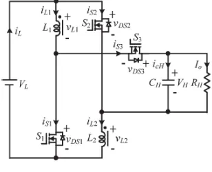
However, their circuit configurations square measure difficult. Fig. 3.1 shows the traditional bifacial dc–dc boost/buck device that is easy structure and simple management. However, the increase and decrease voltage gains square measure low. A changed dc–dc boost device is conferred [26]. The voltage gain of this device is over the traditional dc–dc boost device. Supported this device, a completely unique bifacial dc–dc device is planned, as shown in Fig.3.2. The planned device employs a coupled inductance with same winding turns within the primary and secondary sides.
Fig. 2.3. Proposed converter in step-up mode.
Comparing to the projected convertor and therefore the standard biface boost/buck convertor, the projected convertor has the subsequent advantages: 1) Higher change of magnitude and change of magnitude voltage gains and 2) lower average worth of the switch current beneath same electrical specifications. The subsequent sections can describe the in operation principles and steady-state analysis for the change of magnitude and change of magnitude modes. so as to investigate the steady-state characteristics of the projected convertor, some conditions are assumed: The ON-state resistance RDS(ON) of the switches and therefore the equivalent series resistances of the coupled electrical device and electrical condensers are ignored; the electrical condenser is sufficiently large; and therefore the voltages across the capacitor is treated as constant.
2.1 Step-Up Mode:
The projected device in change of magnitude mode is shown in Fig. 3. The pulse width modulation (PWM) technique is employed to manage the switches S1 and S2 at the same time. The switch S3 is that the synchronous rectifier. Since the first and coil turns of the coupled electrical device is same, the inductance of the coupled electrical device within the primary and secondary sides area unit expressed as
Thus, the mutual inductance M of the coupled inductor is given by:
Where k is the coupling coefficient of the coupled inductor. The voltages across the primary and secondary windings of the coupled inductor are as follows:
Fig.3.4 shows some typical waveforms in continuous
conductivity mode (CCM) and discontinuous
conductivity mode (DCM). The in operation principles and steady-state analysis of CCM and DCM area unit delineated as follows.
2.1.1. CCM Operation
1) Mode 1: During this time interval [t0, t1], S1 and S2 are turned on and S3 is turned off. The current flow path is shown in Fig. 3.5(a). The energy of the low-voltage side VL is transferred to the coupled inductor. Meanwhile, the primary and secondary windings of the coupled inductor are in parallel. The energy stored in the capacitor CH is discharged to the load. Thus, the voltages across L1 and L2 are obtained as
Substituting (3) and (4) into (5), yielding
2) Mode 2: During this time interval [t1, t2], S1 and S2 are turned off and S3 is turned on. The current flow path is shown in Fig. 3.5(b). The low-voltage side VL and the coupled inductor are in series to transfer their energies to the capacitor CH and the load. Meanwhile, the primary and secondary windings of the coupled inductor are in series. Thus, the following equations are found to be
Substituting (3), (4), and (7) into (8), yielding
[image:3.595.325.543.177.249.2] [image:3.595.93.247.275.400.2]International Journal of Emerging Technology and Advanced Engineering
Website: www.ijetae.com (ISSN 2250-2459, ISO 9001:2008 Certified Journal, Volume 3, Issue 12, December 2013)
269
Simplifying (10), the voltage gain is given as
2.1.2. DCM Operation
1) Mode 1:During this time interval [t0, t1], S1 and S2
are turned on and S3 is turned off. The current flow path
[image:4.595.317.541.114.326.2]is shown in Fig. 3.5(a). The operating principle is same as that for the mode 1 of CCM operation. From (6), the two peak currents through the primary and secondary windings of the coupled inductor are given by
[image:4.595.53.274.327.574.2]Fig. 2.4. Some typical waveforms of the proposed converter in step-up mode. (a) CCM operation. (b) DCM operation.
Fig. 2.5. Current flow path of the proposed converter in step-up mode. (a) Mode 1. (b) Mode 2. (c) Mode 3 for DCM operation.
2) Mode 2: During this time interval [t1, t2], S1 and S2 are turned off and S3 is turned on. The current flow path is shown in Fig. 5(b). The low-voltage side VL and the coupled inductor are in series to transfer their energies to the capacitor CH and the load. Meanwhile, the primary and secondary windings of the coupled inductor are in series. The currents iL1 and iL2 through the primary and secondary windings of the coupled inductor are decreased to zero at t = t2. From (9), another expression of IL1p and IL2p is given by
International Journal of Emerging Technology and Advanced Engineering
Website: www.ijetae.com (ISSN 2250-2459, ISO 9001:2008 Certified Journal, Volume 3, Issue 12, December 2013)
270
From Fig. 3.4(b), the average value of the output capacitor current during each switching period is given by
Substituting (12) and (14) into (15), IcH is derived as
Since IcH is equal to zero under steady state, (16) can be rewritten as follows:
Then, the normalized inductor time constant is defined as
Where fs is the switching frequency. Substituting (18) into (17), the voltage gain is given by
2.2. Step-Down Mode
Fig. 3.7 shows the proposed converter in step-down mode. The PWM technique is used to control the switch
S3. The switches S1 and S2 are the synchronous
rectifiers. Fig. 3.8 shows some typical waveforms in CCM and DCM. The operating principle and steady-state analysis of CCM and DCM are described as follows.
2.2.1. CCM Operation
1) Mode 1: During this time interval [t0, t1], S3 is
turned on and S1/S2 are turned off. The current flow path
is shown in Fig. 3.9(a). The energy of the high-voltage
side VH is transferred to the coupled inductor, the
capacitor CL, and the load. Meanwhile, the primary and
secondary windings of the coupled inductor are in series. Thus, the following equations are given as:
[image:5.595.327.540.156.390.2]Substituting (3), (4), and (21) into (22), yielding
[image:5.595.327.536.418.606.2]Fig. 2.6. Some typical waveforms of the proposed converter in step-down mode. (a) CCM operation. (b) DCM operation.
Fig. 2.7. Current flow path of the proposed converter in step-down mode. (a) Mode 1. (b) Mode 2. (c) Mode 3 for DCM operation.
2) Mode 2: During this time interval [t1, t2], S3 is turned off and S1/S2 are turned on. The current flow path is shown in Fig. 3.9(b). The energy stored in the coupled inductor is released to the capacitor CL and the load. Meanwhile, the primary and secondary windings of the coupled inductor are in parallel.
International Journal of Emerging Technology and Advanced Engineering
Website: www.ijetae.com (ISSN 2250-2459, ISO 9001:2008 Certified Journal, Volume 3, Issue 12, December 2013)
271
Substituting (3) and (4) into (24), yielding
By using the state space averaging method, the following equation is obtained from (23) and (25):
Simplifying (26), the voltage gain is found to be
2.2.2. DCM Operation
The operating modes can be divided into three modes, defined as modes 1, 2, and 3.
1) Mode 1: During this time interval [t0, t1], S3 is
turned on and S1/S2 are turned off. The current flow path
is shown in Fig. 3.9(a). The operating principle is same as that for the mode 1 of CCM operation. From (23), the two peak currents through the primary and secondary windings of the coupled inductor are given by
2) Mode 2: During this time interval [t1, t2], S3 is
turned off and S1/S2 are turned on. The current flow path
is shown in Fig. 3.9(b). The energy stored in the coupled
inductor is released to the capacitor CL and the load.
Meanwhile, the primary and secondary windings of the
coupled inductor are in parallel. The currents iL1 and iL2
through the primary and secondary windings of the
coupled inductor are decreased to zero at t = t2. From
(25), another expression of IL1p and IL2p is given as
3) Mode 3: During this time interval [t2, t3], S3 is still
turned off and S1/S2 are still turned on. The current flow
path is shown in Fig.3. 9(c). The energy stored in the
coupled inductor is zero. Thus, iL1 and iL2 are equal to
zero. The energy stored in the capacitor CL is discharged
to the load. From (28) and (29), D2 is derived as follows:
[image:6.595.335.533.123.338.2]From Fig. 3.9(b), the average value of the output capacitor current during each switching period is given by
Fig. 2.8. Boundary condition of the proposed converter in step-down mode (assuming k = 1).
Substituting (28) and (30) into (31), IcL is derived as
Since IcL is equal to zero under steady state, (32) can
be rewritten as follows:
Then, the normalized inductor time constant is defined as
Substituting (34) into (33), the voltage gain of DCM operation is given by
III. CONCLUSION
International Journal of Emerging Technology and Advanced Engineering
Website: www.ijetae.com (ISSN 2250-2459, ISO 9001:2008 Certified Journal, Volume 3, Issue 12, December 2013)
272
At full-load condition, the measured potency is ninety two.7% in accelerate mode and is ninety three.7% in decrease mode. Also, the measured potency is around ninety two.7%–96.2% in change of magnitude mode and is around ninety three.7%–96.7% in decrease mode, that area unit more than the traditional two-way boost/buck convertor.
REFERENCES
[1] M. B. Camara, H. Gualous, F. Gustin, A. Berthon, and B. Dakyo, “DC/DC converter design for supercapacitor and battery power management in hybrid vehicle applications—Polynomial control strategy,” IEEE Trans. Ind. Electron., vol. 57, no. 2, pp. 587–597, Feb. 2010.
[2] T. Bhattacharya, V. S. Giri, K. Mathew, and L. Umanand, “Multiphase bidirectional flyback converter topology for hybrid electric vehicles,” IEEE Trans. Ind. Electron., vol. 56, no. 1, pp. 78–84, Jan. 2009.
[3] Z. Amjadi and S. S. Williamson, “A novel control technique for a switched-capacitor-converter-based hybrid electric vehicle energy storage system,” IEEE Trans. Ind. Electron., vol. 57, no. 3, pp. 926–934, Mar.
[4] F. Z. Peng, F. Zhang, and Z. Qian, “A magnetic-less dc–dc converter for dual-voltage automotive systems,” IEEE Trans. Ind. Appl., vol. 39, no. 2, pp. 511–518, Mar./Apr. 2003.
[5] A. Nasiri, Z. Nie, S. B. Bekiarov, and A. Emadi, “An on-line UPS system with power factor correction and electric isolation using BIFRED converter,” IEEE Trans. Ind. Electron., vol. 55, no. 2, pp. 722–730, Feb.
[6] L. Schuch, C. Rech, H. L. Hey, H. A. Grundling, H. Pinheiro, and J. R. Pinheiro, “Analysis and design of a new high-efficiency bidirectional integrated ZVT PWM converter for DC-bus and battery-bank interface,” IEEE Trans. Ind. Appl., vol. 42, no. 5, pp. 1321–1332, Sep./Oct. 2006.
[7] X. Zhu, X. Li, G. Shen, and D. Xu, “Design of the dynamic power compensation for PEMFC distributed power system,” IEEE Trans. Ind. Electron., vol. 57, no. 6, pp. 1935–1944, Jun. 2010. [8] G. Ma, W. Qu, G. Yu, Y. Liu, N. Liang, and W. Li, “A
zero-voltageswitching bidirectional dc–dc converter with state analysis and softswitching- oriented design consideration,” IEEE Trans. Ind. Electron., vol. 56, no. 6, pp. 2174–2184, Jun. 2009.
[9] F. Z. Peng, H. Li, G. J. Su, and J. S. Lawler, “A new ZVS bidirectional dc–dc converter for fuel cell and battery application,” IEEE Trans. Power Electron., vol. 19, no. 1, pp. 54– 65, Jan. 2004.
[10] K. Jin, M. Yang, X. Ruan, and M. Xu, “Three-level bidirectional converter for fuel-cell/battery hybrid power system,” IEEE Trans. Ind. Electron., vol. 57, no. 6, pp. 1976–1986, Jun. 2010.
[11] R. Gules, J. D. P. Pacheco, H. L. Hey, and J. Imhoff, “A maximum power point tracking system with parallel connection for PV stand-alone applications,” IEEE Trans. Ind. Electron., vol. 55, no. 7, pp. 2674–2683, Jul. 2008.
[12] Z. Liao and X. Ruan, “A novel power management control strategy for stand-alone photovoltaic power system,” in Proc. IEEE IPEMC, 2009, pp. 445–449.
[13] S. Inoue and H. Akagi, “A bidirectional dc–dc converter for an energy storage system with galvanic isolation,” IEEE Trans. Power Electron., vol. 22, no. 6, pp. 2299–2306, Nov. 2007. [14] L. R. Chen, N. Y. Chu, C. S. Wang, and R. H. Liang, “Design of a
International Journal of Emerging Technology and Advanced Engineering
Website: www.ijetae.com (ISSN 2250-2459, ISO 9001:2008 Certified Journal, Volume 3, Issue 12, December 2013)
273
About the Authors:
M. Narender Reddy, Obtained his B.Tech Degree from JNTU in 2002, and he has done his post graduation in power electronics and Industrial drives in 2008 from J.N.T.U Hyderabad. He is currently pursuing Ph.D in energy systems, J.N.T.U Hyderabad. His research interests are in the area Energy systems, Power electronics and electrical machines. Presently, he is working as Associate professor and also heading the department of EEE at Aurora’s Scientific, Technological & Research academy Hyderabad Andhra Pradesh, India. As the head of Department in he has published several papers and also organized various workshops for the benefit of the students.
Mr. P. Sravan kumar, at present is a Sr. Assistant Professor department of Electrical & Electronics Engineering, Aurora’s Scientific, Technological & Research academy Hyderabad Andhra Pradesh, India. He received B.Tech. degree in Electrical and Electronics Engineering from J.N.T.U Hyderabad in2008 , M.Tech (Power Electronics) from J.N.T.U, Hyderabad India He published several papers in various National, International Conferences and Journals. His research interests accumulate in the area of Power Electronics, DC-DC Converters, and Renewable energy sources and Electrical Machines.