© 2016, IRJET | Impact Factor value: 4.45 | ISO 9001:2008 Certified Journal
| Page 872
OMNIDIRECTIONAL PHOTONIC BAND GAP EXPANSION IN GRAPHENE
BASED ONE DIMENSIONAL PHOTONIC CRYSTALS
Neetika Arora
Electronics & communication Department Noida International University,
Noida, India
Prof. S.P.Ojha
Electronics & communication Department , Former Head, Deptt. of Applied Physics, IIT BHU
---***---Abstract-A simple design of one dimensional photonic crystal has been proposed. In this structure alternate layers of Graphene and Silica has been arrange in periodic manner. As graphene has low refractive index whereas silica has high. Here the structure considered has three stacks of five alternate layers of Graphene and silica. For numerical computation transfer matrix method has been used. In this paper, as we increase the thickness of layers (gradual constant ϒ) gradually in each stack we will get wider reflection bands in comparison to a structure with Sio2 and Si layers.
Keywords—Photonic crystal; Graphene; transfer matrix; gradual costant.
Introduction
Photonic crystals are multidimensional periodic structures. The period is of the order of optical wavelength. They have many similarities to solid state crystals. The most important among them is a powerful theory of band of photons, to understand the behavior of light in a complex photonic crystal structure. With the help of it we can create the photonic band gap and the localization of light. They have great applications in optics, optoelectronics, µ-wave technologies, quantum engineering, and bio-photonics and in many other fields.
In a one-dimensional photonic crystal, to achieve a band gap in single direction layers of different dielectric constant can be arrange or adhered together .A Bragg grating is a perfect example of such type of photonic crystal. One-dimensional photonic crystals can be either isotropic or anisotropic, latter one can be used as optical switch .To form a One-dimensional photonic crystal we can arrange infinite number of parallel alternating layers filled with a metamaterial and dielectrics. This can produced identical PBG structures for TE and TM modes.
In photonic crystal the arrangement of refractive index variation controls the movement of photon through the crystal. Here we are considering the graded material .ln graded photonic crystal refractive indices of the alternate layers or their thickness can be varied.
Here we are considering the structure having alternate layers of graphene and silica. Graphene refractive index depends upon the number of layers that has been used. Here there are three stacks of five alternate layers of graphene and silica. Silica is used as a dielectric its refractive index is higher than graphene.
As shown in Figure1, along x axis the alternate layers of graphene and silica have been arranged .there are three stacks of five layers each. The whole setup is placed between semi-infinite media of refractive indices ni (refractive index of the incident medium) and ns (refractive index of the substrate)
By using TMM, the characteristic matrices for the TE and TM waves is given by
Mj= (1)
Where qj= njcosθj, (j = 1, 2; for the first and the second layers of theunit cell respectively) for TE polarization
qj= cosθj/nj and for TM polarization, βj =
(2π/λ)njdjcosθj , θj is the ray angle insidethe layer of refractive index nj and λ is the wavelength in the mediumof incidence. The total characteristic matrix for the N periods of thestructure can be given as
M = (M1 ×M2)N = (2)
© 2016, IRJET | Impact Factor value: 4.45 | ISO 9001:2008 Certified Journal
| Page 873
r = (3)
[image:2.595.38.280.202.352.2] [image:2.595.333.588.527.724.2]where qi,s= ni,scosθj,sfor TE wave and qi,s= cosθj,s/ ni,sfor TM wave, where the subscripts i and s refers to the quantities of the incident medium and substrate respectively.The reflectivity of the structure can be expressed as
R = |r|2 (4)
Fig 1. Schematic representation of GSPC structure In The edges of PBG will shift towards the higher frequency side as we increase the angle of incidence and at brewester angle TM mode do not reflects.these are the two important factor because of them there is no absolute photonic band gap (PBG) but it does not mean that there is no Omni-directional reflection. The criterion for the existence of total Omni-directional reflection is that incident wave should no couple with any of propagating modes
From Snell’s law,
We know ni sin θi = n1 sin θ1 and n1 sin θ1 = n2 sin θ2
i.e., θ1 =sin−1(ni sin θi/n1) and θ2 = sin−1(n1 sin θ1/n2)
Where n1 and n2 are the refractive indices of the low and high index media respectively and ni is the refractive index of the incident medium. The maximumrefracted angle is defined as θmax2 = sin−1(ni / n2) and Brewster angles θB = tan−1(n1sinθ/ n2). The incident wave from outside cannot couple to Brewster’s window If the maximum refracted angle is smaller than the Brewster’s angle which results to total reflection for all incident angles. so, the condition for Omni-directional reflection without the influence of the Brewster’s angle is θB = θmax2 [23].This condition is satisfied by the selected parameters that we are using for our numerical calculations. Hence, in the given
observations there is no influence of Brewster’s angle on the Omni-directional reflection bands.
Result & discussion
From the computation of Equation (3), the reflection properties of one-dimensional GSPC can be expressed asgraphically.For the analysis , we consider a GSPC structure with the following sequence — air/(AB)5/(A1B1)5/(A2B2)5/ Substrate(SiO2). For AB stack, we have chosen graphene as the material of layer A and the material of layer B as SiO2 having refractive indices 2.1 and 3.7 respectively the refractive index of graphene depends on number of layers we are using .All the regions are considered to be non-absorbing ,linear and homogeneous. Also, the refractive indices of both the materials are considered to be constant throughout the structure. The thickness of the layers are considered as a = 283nm and b = 115 nm. As per the quarter wave stack condition a = λC/4n1 and b = λC /4n2, where λC
(= 1700 nm) is the critical wavelength.it is the mid wavelength of the whole wavelength range. For A1B1 stack, we choose the material of layer A1 as Graphene and the material of layer B1 as Sio2 in which the thicknesses of the layers A1 and B1 are taken as a1 = ϒa and b1 = ϒb respectively, where ϒ is defined as gradual constant. In a similar way, we choose the material of layer A2 as Graphene and the material of layer B2 as Si in which the thicknesses of layers A2
and B2 are taken as a2 = ϒ a1 and b2 = ϒ b1
respectively. The reflectance spectra for conventional PC can
Be obtained by choosing y=1 in this structure.
© 2016, IRJET | Impact Factor value: 4.45 | ISO 9001:2008 Certified Journal
| Page 874
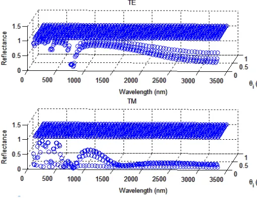
Fig 3. Reflectance spectra of SiO2/Sione-dimensional PC (ϒ = 1.1) for TE and TM polarizations.
Fig 4. Reflectance spectra of SiO2/Si one-dimensional PC (ϒ = 1.2) for TE and TM polarizations.
We observe from Table that the TE polarization has its Omni- directional reflection range from 1289 nm
to 2210 nm and the Omni- directional reflection range for the TM polarization from 1289 nm to 1929 nm. Therefore, the total ODR for both TE and TM polarizations when ϒ = 1, i.e., for the case of conventional PC, has the bandwidth (Δλ = λH − λL) of
640 nm. The upper wavelength edge of the ODR band is λH = 1929 nm and the lower wavelength edge is λL
= 1289 nm. Hence, the normalized Omni-directional bandwidth is 37.65% of the total wavelength range considered around the critical wavelength λC = 1700
nm.
TABLE 1. Total reflection region and gap width for SiO2/Si one- dimensional PC (ϒ = 1).
For γ = 1.1, the reflectance spectra and photonic band structure of one-dimensional GSPC for both TE and TM polarizations are shown in Figures 3 and the corresponding ODR data are tabulated in Table 2. We observe from these figures and table that the TE polarization has its ODR range from 1345 nm to 2745 nm and the ODR range for the TM polarization is from 1345 nm to 2288 nm. Therefore, the total ODR (for both TE and TM polarizations) in the case of GSPC structure with γ = 1.1, has a bandwidth of 943 nm. The upper wavelength edge of ODR band is λH = 2288 nm and the lower wavelength edge of the ODR is λL= 1345 nm. Thus, the normalized omni-directional bandwidth is ∆λ/ λc = 55.4% of the total wavelength range considered around the critical wavelength λc = 1700 nm. That is the ODR range of one-dimensional GSPC when γ = 1.1 is 1.48 times of ODR range of conventional PC (γ = 1).
TABLE 2. Total reflection region and gap width for SiO2/Si one- dimensional PC (ϒ = 1.1)
Angle of incidence ᶿi (degree)
TE polarization TM polarization
Reflecti on range (nm)
Gap width
(nm)
Reflec tion range (nm)
Gap width(n m)
0 1345–
2930
1585 1365–
2910
1545
30 1311–
2905
1594 1307–
2712
1405
60 1154– 1635 1245– 1154
Angle of incidence θi
(degree)
TE polarization TM polarization
Reflection range (nm)
Gap width(nm)
Reflection range (nm)
Gap width(nm)
0 1289–
2342
1053 1289–
2342
1053
30 1252–
2379
1127 1298–
2284
986
60 1210–
2302
1092 1192–
1971
779
85 1117–
2210
1093 1197–
1929
[image:3.595.31.318.105.471.2] [image:3.595.36.290.534.679.2] [image:3.595.314.565.538.792.2]© 2016, IRJET | Impact Factor value: 4.45 | ISO 9001:2008 Certified Journal
| Page 875
2789 2399
85 1106–
2745
1639 1250–
2288
1038
Also for γ = 1.2, the reflectance spectra and photonic band structure of GSPC structure for both TE and TM polarizations are shown in Figures 4 and the corresponding ODR data are tabulated in Table 3. From these Figures and Table, we observe that the TE polarization has its ODR range from 1342 nm to 3103 nm and the ODR range for TM polarization is from 1342 nm to 2376 nm. Therefore, total ODR (for both TE and TM polarizations) in the case of GSPC structure with γ = 1.2, has the bandwidth 1395 nm. The upper wavelength edge of ODR band is λH = 2566 nm and the lower wavelength edge of the ODR is λL = 1171 nm. Thus the normalized omni-directional bandwidth is 82.1% of the total wavelength range considered around the critical wavelength λ = 1700 nm. That is, the ODR range of GSPC in the case when γ = 1.2, is 1.48 times of ODR range for γ = 1.1 and 2.2 times of ODR range of γ = 1.
[image:4.595.325.566.173.444.2]Finally, by increasing the value of gradual constant γ in steps 0.01, the variation in ODR range with gradual constant (γ) is plotted as shown in Figure 8. Here, the gap between two dotted lines shows the ODR range for a particular value of γ.
Table 3. Total reflection region and gap width for SiO /Graphene onedimensional GSPC (γ = 1.2).
conclusion
To summarize, we have investigated theoretically the ODR range of one-dimensional GSPC structure. It is found that the ODR range of GSPC structure can be enhanced by changing the material si by Graphene with constant the value of gradual constant and that the ODR range for one-dimensional GSPC structure is more than that of conventional PC and simple graded structure. Hence, a one-dimensional GSPC structure can be used as a broadband optical reflector, and the range of reflection can be tuned to a desired wavelength region by changing the material by Graphene and also by choosing proper thickness of the period (d) of first stack and relative thicknesses of individual layers of the following stacks. These types of optical reflectors are compact in size and may have potential applications in the field of optical technology and optoelectronics.
Angle
of incide nce ᶿi
(degre e)
TE polarization TM polarization
Reflecti on range (nm)
Gap width(n m)
Reflection range (nm)
Gap width( nm)
0 1171–
3312
2141 1171–
3312
2141
30 1067–
3309
2242 1115–
3261
2146
60
1045-3239
2194 1005–
2627
1622
85 1013–
3213
2200 1123–
2566
© 2016, IRJET | Impact Factor value: 4.45 | ISO 9001:2008 Certified Journal
| Page 876
References[1] Yablonovitch, E., “Inhibited spontaneous emission in solid-state physics and electronics,” Phys. Rev. Lett., Vol. 58, 2059–2062, 1987. [2] John, S., “Strong localization of photons in certain
disordered dielectric superlattices,” Phys. Rev. Lett., Vol. 58, 2486–2489, 1987.
[3] Jonnopoulos, J. D., P. Villeneuve, and S. Fan, “Photonic crystals: Putting a new twist on light,” Nature, Vol. 386, 143–149, 1997.
[4] Xu, K. Y., X. Zheng, C. L. Li, and W. L. She, “Design of omnidirectional and multiple channeled filters using one- dimensional photonic crystals containing a defect layer with a negative refractive index material,” Phys. Rev. E, Vol. 71, 066604, 2005.
[5] Singh, S. K., J. P. Pandey, K. B. Thapa, and S. P. Ojha, “Some new band gaps and defect modes of one dimensional photonic crystals composed of etamaterials,” Solid State Commun., Vol. 143, 217, 2007.
[6] St. J. Russell, P., S. Treadwell, and P. J. Roberts, “Full photonic band gap and spontaneous emission control in 1D multilayer dielectric structures,” Opt. Commun., Vol. 160, 66–71, 1999.
[7] Kumar, V., K. S. Singh, and S. P. Ojha, “Band structures, reflection properties and abnormal behaviour of one-dimensional plasma photonic crystals,” Progress In Electromagnetics Research M, Vol. 9, 227–241, 2009.
[8] Pandey, G. N., K. B. Thapa, S. K. Srivastava, and S. P. Ojha, “Band structures and abnormal behaviour of one dimensional photonic crystal containing negative index materials,” Progress In Electromagnetics Research M, Vol. 2, 15–36, 2008.
[9] Dowling, J. P., “Mirror on the wall: You’re omnidirectional after all?,” Science, Vol. 282, 1841–1842, 1998.
[10] Yablonovitch, E., “Engineered omnidirectional external- reflectivity spectra from one-dimensional layered interference filters,” Opt. Lett., Vol. 23, 1648–1649, 1998.
[11] Chigrin, D. N., A. V. Lavrinenko, D. A. Yarotsky, and S. V. Gaponenko, “Observation of total omnidirectional reflection from a one dimensional dielectric lattice,” Appl. Phys. A: Mater.Sci. Process., Vol. 68, 25–28, 1999.
[12] Fink, Y., J. N. Winn, S. Fan, C. Chen, J. Michel, J. D. Joannopoulos, and E. L. Thomas, “A dielectric
omni- directional reflector,” Science, Vol. 282, 1679–1682, 1998.
[13] Lusk, D., I. Abdulhalim, and F. Placido, “Omnidirectional reflection from Fibonacci quasi-periodic one-dimensional photonic crystal,” Opt. Commun., Vol. 198, 273–279, 2001.
[14] Ibanescu, M., Y. Fink, S. Fan, E. L. Thomas, and J. D. Joannopoulos, “An all-dielectric coaxial waveguide,” Science , Vol. 289, 415–419, 2000. [15] Srivastava, S. K. and S. P. Ojha, “Omnidirectional
reflection bands in one-dimensional photonic crystal structure using fullerence films,” Progress In Electromagnetics Research, Vol. 74, 181–194, 2007.
[16] Srivastava, R., S. Pati, and S. P. Ojha, “Enhancement of omnidirectional reflection in photonic crystal heterostructures,” Progress In Electromagnetics Research B, Vol. 1, 197–208, 2008.
[17] Huang, J. P. and K. W. Yu, “Optical nonlinearity enhancement of graded metallic films,” Appl. Phys. Lett., Vol. 85, 94–96, 2004.
[18] Sang, Z. F. and Z. Y. Li, “Effective negative refractive index of graded granular composites with metallic magnetic particles,” Phys. Lett. A, Vol. 334, 422–428, 2005.
[19] Huang, J. P. and K. W. Yu, “Second-harmonic generation in graded metallic films,” Opt. Lett., Vol. 30, 275–277, 2005.
[20] Yeh, P., Optical Waves in Layered Media, John Wiley and Sons, New York, 1988.
[21] Born, M. and E. Wolf, Principle of Optics, 4th edition, Pergamon , Oxford, 1970.
[22] Winn, J. N., Y. Fink, S. Fan, and J. D. Joannopoulos, “Omni- directional reflection from a one-dimensional photonic crystal,” Optics Lett., Vol. 23, 1573–1575, 1998.
[23] Lee, H. Y. and T. Yao, “Design and evaluation of omnidirectional one- dimensional photonic crystals,” J. Appl. Phys., Vol. 93, 819– 837, 2003. [24] Srivastava, S. K. and S. P. Ojha, “Broadband