DEVELOPMENT OF TIME DELAY CURRENT CONTROL FOR LEAD ACID BATTERY 12 V DC BY USING ARDUINO
NURUL SYAZRAH BINTI MAT YATIM
The thesis is to submit in
fulfillment of the requirement for the award of Degree of Master Electrical Engineering
Faculty of Electrical and Electronic Engineering Universiti Tun Hussein Onn Malaysia
ABSTRACT
ABSTRAK
CONTENTS
TITLE I
DECLARATION II
DEDICATION III
ACKNOWLEDGEMENT IV
ABSTRACT V
ABSTRAK VI
CONTENTS VII
LISTOFFIGURES IX
LISTOFTABLES XII
LISTOFSYMBOLSANDABBREVIATIONS XIII
CHAPTER 1 1
INTRODUCTION 1
1.1 Project Background 1
1.2 Problem Statement 3
1.3 Objectives 3
1.4 Research Scope 4
CHAPTER 2 5
LITERATUREREVIEW 5
2.1 A Brief Review of Battery 5
2.2 Single – Phase Buck – Boost Converter 8
2.3 Control Method between Buck-Boost and Battery 10
2.4 Time Delay Control 19
CHAPTER 3 23
RESEARCHMETHODOLOGY 23
3.1 Block Diagram of the Project 23
3.2 Flowchart of System 24
3.3 Project Development 26
CHAPTER 4 38
RESULTANDDISCUSSION 38
4.1 Open Loop Simulation Diagram and Result 38
4.2 Closed Loop Simulation Diagram and Result 44
4.3 Open Loop Hardware and Result 49
4.4 Closed Loop Hardware and Result 59
CHAPTER 5 65
CONCLUSIONANDRECOMMENDATION 65
5.1 Conclusion 65
5.2 Recommendations 66
REFERENCES 67
VITA 70
APPENDIX A 71
APPENDIX B 73
LIST OF FIGURES
Figure 1.1: Block diagram of battery charger system 2
Figure 2.1: Load curve for Kyushu region in Japan August,2011 8
Figure 2.2: System block diagram 9
Figure 2.3: Photovoltaic power system 10
Figure 2.4: The Conventional dynamic model of buck - boost converter. 10 Figure 2.5: Scheme of voltage-mode controlled boost DC/DC converter 11 Figure 2.6: Time-delay introduced by PWM in voltage-mode control 12 Figure 2.7: Scheme of current-mode controlled boost DC/DC converter 12 Figure 2.8: Illustration of the stability of current loop is stable when D < 0.5 13
Figure 2.9: Common Buck – Boost circuit 13
Figure 2.10: Common Buck circuit 14
Figure 2.11: Common Boost circuit 14
Figure 2.12 : Inductor current versus time 15
Figure 2.13: Ridley‟s model of the time-delay controller. 19
Figure 2.14: The Arduino board 22
Figure 3.1: Block diagram of time delay control current for battery. 23
Figure 3.2: Flowchart of the lead acid battery charger 24
Figure 3.3: The time delay control closed loop 25
Figure 3.4: Buck – Boost converter circuit layout 26
Figure 3.5: Hardware of Buck-Boost converter circuit. 27
Figure 3.6: Boost circuit diagram in buck – boost circuit 28
Figure 3.7 : Buck condition in Buck – boost circuit 29
Figure 3.8: Gate driver layout 32
Figure 3.9: Hardware of Gate driver circuit 33
Figure 3.10: Current sensor 50A layout 34
Figure 3.12: Voltage sensor circuit 36
Figure 3.13: Experiment set up 37
Figure 4.1: Boost circuit diagram in buck – boost circuit 39
Figure 4.2: Open loop simulation diagram 39
Figure 4.3: AND and OR gates block diagram 40
Figure 4.4: The simulink model of arduino for open loop diagram 41 Figure 4.5: Output waveform of the gate driver when boost operation 41 Figure 4.6: Output waveform of the gate driver when buck operation 42 Figure 4.7: The output current for open loop simulation waveform 43
Figure 4.8: Closed loop simulation diagram 44
Figure 4.9: The Simulink model for closed loop 45
Figure 4.10: The simulink model for the Analog to Digital converter (ADC) 45 Figure 4.11: The simulink model for current sensor by time delay control 46 Figure 4.12: The output current for closed loop simulation waveform 47 Figure 4.13: Pin 11 – constant input waveform when boost condition 49 Figure 4.14: Pin 9 – PWM input waveform when boost condition 50 Figure 4.15: Pin 11 – zero input waveform when buck condition 50 Figure 4.16: Pin 9 – PWM input waveform when buck condition 51
Figure 4.17: A switch SW1 output when boost condition 51
Figure 4.18: A switch SW2 output when boost condition 52
Figure 4.19: A switch SW1 output when buck condition 52
Figure 4.20: A switch SW2 output when buck condition 53
Figure 4.21: Graph Vout when Vin=10V 53
Figure 4.22: Graph Vout when Vin=11V 53
Figure 4.23: Graph Vout when Vin=12V 54
Figure 4.24: Graph Vout when Vin=13V 54
Figure 4.25: Graph Vout when Vin=14V 54
Figure 4.26: Graph Vout when Vin=15V 54
Figure 4.27: Graph Vout when Vin=16V 55
Figure 4.28: Graph Vout when Vin=17V 55
Figure 4.30: The open loop hardware waveform 56 Figure 4.31: Graph IV characteristic for open loop hardware 58
Figure 4.32: Closed Loop Hardware set up 59
Figure 4.33: Graph Vout when Vin=10V 60
Figure 4.34: Graph Vout when Vin=11V 60
Figure 4.35: Graph Vout when Vin=12V 60
Figure 4.36: Graph Vout when Vin=13V 60
Figure 4.37: Graph Vout when Vin=14V 61
Figure 4.38: Graph Vout when Vin=15V 61
Figure 4.39: Graph Vout when Vin=16V 61
Figure 4.40: Graph Vout when Vin=17V 61
Figure 4.41: Graph Vout when Vin=18V 62
Figure 4.42: The closed loop hardware waveform 62
LIST OF TABLES
Table 2.1: The comparison between rechargeable batteries 6
Table 2.2: The pros and cons of each charging method 18
Table 3.1: List of component for buck-boost circuit 27
Table 3.2: Switch condition for boost operation 28
Table 3.3: Parameter characteristic for Boost circuit 29
Table 3.4: Switch condition for buck operation 30
Table 3.5: Parameter characteristic for Buck circuit 31
Table 3.6: Lists of components for gate driver circuit 33
Table 4.1: Truth table of OR gate 40
Table 4.2: Truth table of AND gate 40
Table 4.3: Open loop simulation result 43
Table 4.4: Closed loop simulation result 47
Table 4.5: The simulation result 48
Table 4.6: Open loop simulation and hardware result 57
LIST OF SYMBOLS AND ABBREVIATIONS
r,r(t) - Reference input
e,e(t) - Error between the input signal and the output u,u(t) - Input applied by the controller to plant y, y(t) - Output of the closed loop control system Gp(s) - Plant transfer function
Gc(s) - Controller transfer function
Gd(s) - Disturbance input to output transfer function H(s) - Feedback measurement
Dt(s) - Disturbance input
va(t) - Input source voltage, [Volt] ia(t) - Armature current, [Ampere] Ra - Armature resistance, [Ohm] La - Electric inductance, [H]
1
i i T -
Homogeneous transformation matrix of I relative to i-1 KP - Proportional gain
KD - Derivative gain KI - Integral gain
TI - Integral time constant TD - derivative time constant tr - Rising time, [sec] ts - Settling time, [sec] μ(u) - Membership function Φ - Null fuzzy set (Phi) Δe - Change of the error ke - Scaling factor for error
kde - Scaling factor for change of error ku - Scaling factor for output
i - Number of links
R - Number of the fuzzy rules
V - Voltage
DC - direct current
PWM - Pulse Width Modulation ADC - Analog to Digital Converter CC - Constant Current
CHAPTER 1
INTRODUCTION
1.1 Project Background
There is a wide variety of batteries on the market today, which are Nickel Cadmium (NiCa/NiCd), Nickel Metal Hydride (NiMH), Lead acid and Lithium Ion (Li-Ion) batteries. The lead-acid battery is widely used as a supply of power because the maintenance is easy and it‟s convenient to be used [1]. However, as the repeated charging and discharging the capacity of lead-acid battery gets decreased, meanwhile, its life span become short as well. It‟s known that the charging process is the most important factor to the working life of lead-acid battery.
Power conversion system is constructed to improve performance or reliability, or attain a high system rating [2]. Energy can flow from the highest cell to the lowest cell with the isolated buck - boost DC – DC converter. The control scheme implements the balancing with the least quantity of switches and cost [3]. Buck - boost converters are frequently used as a battery charging/discharging circuit in many photovoltaic power system, automotive power system and spacecraft power system [4].
Figure 1.1 shows the block diagram of battery charger system which are consists of a power source, the buck – boost DC converter, control system and battery. Power source will supplied an input DC voltage. Then, the voltage will be converting to the stable voltage by using buck -boost DC converter. The control system will be monitoring the data of input voltage and output current. A battery as a load in the battery charging system.
Figure 1.1: Block diagram of battery charger system Buck –
1.2 Problem Statement
To charge batteries, many battery charge strategies have been proposed. The constant-current constant - voltage charge strategy is the most popularly used one these days. However, a battery charge system with a high quality is still desired [5]. The controller such as PID, p-resonant, repetitive and time delay, fuzzy logic control and etc was applied in battery charge systems. Conventional controller has issued in handling charge current to increase battery charging performance.
In electrical vehicle applications power supply systems, the battery charger circuits require an output voltage which is usually less than the input voltage [2]. Regarding the battery condition, the buck – boost converter will work as a current source or as a voltage source. For the controller design the worst case to control switching of buck – boost converter has been taking into consideration. The output from buck – boost converter must be constant compare to an input which is variable.
1.3 Objectives
1. To design the time delay controller of a current controlled
2. To analyze the feedback of open and closed loop using time delay controller. 3. To enhance the performance of the Arduino and MATLAB for signal processing
device interface time.
1.4 Research Scope
1. The size of the battery is 12 V 7 Ah lead acid.
2. The size of bidirectional converter is 10 - 18 V input voltage, 12 V output voltages with filter inductor value is 10mH, Filter capacitor value is 47µF.
3. Perform simulation of time delay controller. This simulation will be carried out on MATLAB platform with Simulink as it user interface.
4. Analyze the performance of time delay controller.
CHAPTER 2
LITERATURE REVIEW
2.1 A Brief Review of Battery
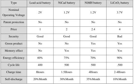
Methods of fast charging of lead acid batteries have been studied and developed for the last 30 years. In 1973, there has been a publication outlining that fast charging has some chemical and physical effects on battery plates, and therefore reduces the battery life. These effects can be seen as gassing and heat generation [6]. It is desirable to be able to rapidly recharge its batteries within one hour or less. As is the case under any charging conditions, it is important to control the charge in order to maintain the batteries in good condition. The rise of temperature, the overcharge and gassing are more prone to occur during high-rate charging, charge control under these conditions is critical.
these batteries, lead- acid battery has a long history and is safe, reliable and affordable[7].
Table 2.1: The comparison between rechargeable batteries
Type Lead-acid battery NiCad battery NiMH battery LiCoO2 battery
Nominal
Operating Voltage 2V 1.2V 1.2V 3.7V
Patent protection No No No No
Price 1 2 2.4 4
Security Good Good Good Bad
Green product No No Yes Yes
Memory effect No Yes Yes Yes
Energy efficiency 60% 75% 70% 90%
Cycle life 400 500 500 .500
Charge time 8hours 1.5Hours 4Hours 2-4Hours
Self-discharge 20%Month 30%Month 35%Month 10%Month
The charge ends when the battery capacity is reached and the battery is going to discharge to register more information about the efficiency of the complete process. The value of capacity for each battery is taken of a database where the battery life is stored. The combined charge strategies is used to obtain a high charge efficiency with considerable reduction of the charge time, as well as keep the battery temperature between reasonable values (maximum value 50ºC) or not exceed the bubbling voltage (7.95 V, in these batteries). If the central cell temperature reaches 50ºC the software pauses the process until the temperature goes down a program value, then the charge is resumed [9].
The cycle-life of lead-acid batteries can indeed be improved by the use of high charge currents. We are working in the development of electronic systems of fast charge lead-acid batteries and so that this system can optimize the yield and the useful life of the battery, it is needed to provide to the battery the necessary load and with the most appropriate strategy [10].
Figure 2.1: Load curve for Kyushu region in Japan August,2011
2.2 Single – Phase Buck – Boost Converter
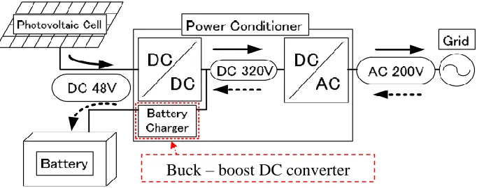
Buck - boost converters are frequently used as a battery charging/discharging circuit in many photovoltaic power systems, automotive power systems, and spacecraft power system. In these applications, bidirectional converters often employ a multi-module structure in order to reduce the ripple component in the battery charging/discharging current. In particular the magnitude of the ripple component can be drastically shrunk by operating power modules with appropriate phase delays in their switch driving signals. This multi-module multi-phase operation reduces the switch current stress and inductor size. In addition, it could substantially improve the battery lifetime and system reliability [4].
Buck converter and boost converter are usually used in maximum power point system because of their simplicity in structure and control scheme. Buck converter can generate a voltage below the input voltage, while boost converter steps up the input voltage to a higher voltage. While they are mostly used in high power PV system, both of them are not suitable for the application of energy-harvesting battery charger. Inverting buck-boost converters and Cuk converters are capable of converting supply voltages to both higher and lower voltages, but the polarity of the output voltage is opposite to the supply voltage, which makes it not applicable for multiple power source system [13].
Figure 2.2: System block diagram
Figure 2.3: Photovoltaic power system
2.3 Control Method between Buck-Boost and Battery
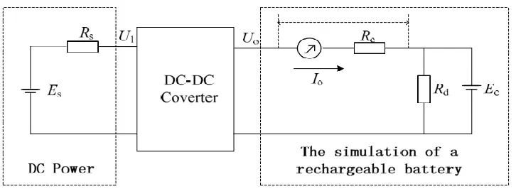
A buck - boost DC – DC converter connects two sources/loads, it has two modes of operation (see Figure2.4): 1- Discharging mode; the power is fed forward from the battery to load. 2-Charging mode; where the power is fed back to the battery.
Figure 2.4: The Conventional dynamic model of buck - boost converter.
Using different takes charging methods influences the life of battery. It spends too much time and cost to charge batteries by the methods which are safe and high efficient according to the service manual that the battery manufacturer offered. Therefore, the characteristics of fast and less influence of the charging methods are proposed successively.
Buck –boost DC converter
Buck –boost DC converter
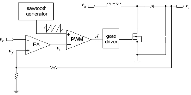
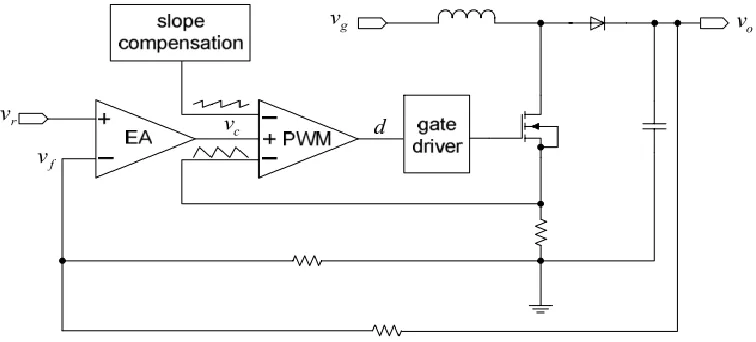
[image:21.612.234.425.373.547.2]As shown in Figure 2.5, there is only the voltage feedback in voltage-mode control. Duty ratio d is determined by the comparison of the sawtooth waveform and the control voltage vc, which is the amplified error of voltage reference vr and the feedback voltage vf. PWM transfers vc to d [15].
Figure 2.5: Scheme of voltage-mode controlled boost DC/DC converter
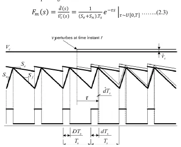
Figure 2.6 illustrates the time-delay τ between vc perturbation and the system response in the form of adjusting d. Thus, PWM in voltage-mode control is modeled as
𝐹
𝑚𝑠 =
𝑑 𝑠𝑣𝑐 𝑠
=
1 𝑆𝑒𝑇𝑠
𝑒
−𝜏𝑠 ………(2.1)
Figure 2.6: Time-delay introduced by PWM in voltage-mode control
The time-delay model of PWM in voltage-mode control
𝐹
𝑚𝑠 =
1𝑆𝑒𝑇𝑠
𝑒
−𝜏𝑠𝜏~𝑈 0,𝑇 ……..(2.2)
[image:23.612.136.514.478.649.2]Figure 2.7 shows that in current-mode control there is an additional current loop inside the outer voltage loop. The duty-ratio is no longer an independent variable but is controlled by the inductor – current iL.
Assume each variable only perturbs in the small-signal limit, Figure 2.8 illustrates that the duty-ratio plays a decisive role in the stability of current loop, which is one of the most important issues of current-mode control. Similar as (2.1), the time-delay model of PWM operating in current-mode control is
𝐹
𝑚𝑠 =
𝑑 𝑠𝑣 𝑠 𝑐
=
1 𝑆𝑒+𝑆𝑛 .𝑇𝑠𝑒
−𝜏𝑠
[image:24.612.144.509.144.441.2]𝜏~𝑈 0,𝑇 ……..(2.3)
Figure 2.8: Illustration of the stability of current loop is stable when D < 0.5
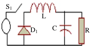
[image:24.612.185.474.603.667.2]Figure 2.9 shows the common buck – boost circuit diagram. This circuit consist two switches, an inductor, two diodes, a capacitor and two resistors. If the input voltage is higher than reference voltage, the circuit will in buck condition as shown in Figure 2.10 while the input voltage is low than reference voltage, the circuit will be in boost condition as shown in Figure 2.11.
Figure 2.9: Common Buck – Boost circuit L
D1
D2 C R
R S2
Figure 2.10: Common Buck circuit
Figure 2.11: Common Boost circuit
For the boost condition, by using Kirchhoff‟s Voltage Law, the voltage across the inductor, VL is given by the difference between voltage supply, Vs and output voltage, Vo.
O S
L V V
V ... (2.4)
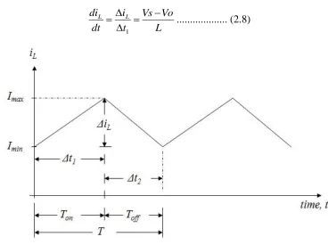
The inductor voltage, VL is related to the change in current flowing through it according to the relation.
dt di L
V L
L ... (2.5)
Equating VL in both equation,
dt di L V V V L O S
L ... (2.6)
L Vo Vs dt
diL
[image:25.612.242.408.232.319.2]Since
dt diL
is constant, the equation can rewrite as below:
L Vo Vs t i dt
diL L
1
[image:26.612.138.506.102.377.2]... (2.8)
Figure 2.12 : Inductor current versus time
The duty cycle, D of the switch is defined as follows:
T T T T T D on off on on
... (2.9)
Equation can be rewritten as below:
L V V DT
iL S O
DT L V V
i S O
L …...(2.10)
For an inductor value,
𝐿
𝑚𝑖𝑛=
𝐷 1−𝐷 2𝑅𝐿For a capacitor value,
𝐶 =
𝐷𝑅𝑓 ∆𝑉𝑜
𝑉𝐷𝐶
………(2.12)
For the buck condition, by using Kirchhoff‟s Voltage Law, the voltage across the inductor, VL is given by the difference between voltage supply, Vs and output voltage, Vo.
O
L V
V ...(2.13)
The inductor voltage, VL is related to the change in current flowing through it according to the relation.
dt di L V L L ...(2.14)
Equating VL in both equation,
dt di L V V L O
L
L Vo dt
diL
...(2.15)
Since
dt diL
is constant, the equation can rewrite as below:
L Vo t
i dt
diL L
2 ...(2.16)
By referring Figure 2.5,
T D T
t2 off (1 )
L Vo T
D iL
T D L
Vo
iL (1 )
...(2.17)
The nett change in inductor current over the period T is zero, this condition requires that
opened i
closed
iL L
Hence, T D L V L V
VS O O
) 1 ( ...(2.18)
Solving for Vo :
S
O DV
V ...(2.19)
For an inductor value,
𝐿𝑚𝑖𝑛 =
1−𝐷 𝑅𝐿2𝑓
…
where given f = 10kHz (2.20)For a capacitor value,
𝐶 =
1−𝐷8𝐿 ∆𝑉𝑂
𝑉𝐷𝐶 𝑓2
Table 2.2: The pros and cons of each charging method
Method Advantage Disadvantage
Constant current method It has ability of limited current to prevent the over current of initial charge
It is easy to overcharge in later stage
Constant voltage method It has ability of limited voltage to prevent the over voltage
It is easy to over current in initial stage
Constant current/constant voltage method
It can limit voltage and current Charge time is too ling
Pulse charge method It can reduce the polarization to prevent the battery temperature rise
Control is complex
Reflex charge method It can reduce the polarization to prevent the battery temperature rise
2.4 Time Delay Control
A controller is a device, possibly in the form of a chip, analogue electronics, or computer, which monitors and physically alters the operating conditions of a given dynamical system. Many controllers have been developed, that can be divided into two classifications, passive and adaptive power controller. The example for passive power controller is hysteresis, relay and sliding mode control and for adaptive power controller is PID, fuzzy, P-resonant, Time delay controller. Each of them has their advantages, such as simple structure and low maintenance cost.
Adaptive controller is a controller that can modify its behavior in response to changes in the dynamics of the process and the disturbances. A great number of industrial control loops are under adaptive control. These include a wide range of applications in aerospace, process control, ship steering, robotics and other industrial control systems [16]
The time delay is generally regarded as a irritation to a control system. Its presence hinders the control system design, limits the achievable performance of a controller, and may trigger serious stability concerns. As the inverse of time delay implies prediction into the future, the resulting controller exhibits predictive characteristics. Essentially, the time delay controller proposed includes a delay element in positive feedback and a reference model in the forward path. In order to solve the problem of adaptive tuning of the time-delay controller, the dynamics of the system are first identified by the polynomial identification [16].
[image:30.612.193.453.568.689.2]The proposed controller uses the delay element in positive feedback with a reference model Gm(s), as shown in Figure 2.13.
The effects of the sampling and computational time delay, which is an inevitable characteristic of digital control systems, and dead-time, which must be inserted to prevent a leg short circuit, influence the ability of a current controller to effectively track the reference current signals. This is especially evident in a shunt active power filter application where the performance is directly dependent on the ability of the converter to effectively track the reference current signals.
The time it takes to sample the current and voltage values and the time that the DSP takes to process the sampled values leads to a 1 sampling period (Ts) time delay between sampling and actually applying the duty cycles to the inverter. This can cause oscillations in the actual current [17].
Lead-acid battery use Traditional Charging Method, they are Constant current, Constant Voltage, constant current constant voltage (CC, CV) and pulse charging constant [18]. Constant currents are used to charge the battery. This method is simple that using current monitoring, however monitoring the voltage of battery is to prevent the over-discharging by higher voltage.
Constant voltage is used to charge the battery. This method is easy to implement but only the initial current required limiting to protect the charger. The drawback of this method is the charging time longer than Constant Current method.
Combine the two methods, CCCV charging method is established. Constant Current is used at initial stage for providing starting charging current. Until the voltage charge up to cutoff or preset voltage, battery is switched to Constant Voltage mode to be a float charge.
2.5 Arduino
A central controller (our Arduino board) receives user commands to execute. It has Internet connectivity through an Ethernet shield mounted on the Arduino. On the user side, a mobile device provides interface with the system as a whole through a user-friendly application. The mobile device can be either wired to the central controller (through USB cable for instance), or communicates with it wirelessly. Within the scope of the home, wireless connectivity can be achieved using an Ethernet shield on the central controller. This way, we would be able to access the controller either locally or remotely through the Internet.
In recent years Arduino – like platforms have seen enormous diffusion both in amateur applications and in research environments due to their simplified programming language and low-cost. The spreading of the new open hardware platform led to an increase of available “interface shields”; this increased furthermore the flexibility of the Arduino platforms which started to spread in most of the academic environments. In the development of control loops for power electronic converters, the platform was not really successful probably due to the limited performances of the microcontrollers which the boards are based on or the lack of availability of suitable interface boards for power electronics.
CHAPTER 3
RESEARCH METHODOLOGY
3.1 Block Diagram of the Project
[image:34.612.159.486.387.580.2]Figure 3.1 shows a simplified block diagram of a typical lead-acid batteries charger system. It consist of 5 mains parts as a DC power source, a buck-boost converter, a custom data acquisition system (current sensor) and a control system (consist of Arduino, Matlab and gate drive) and output (battery 12 – 7 Ah).
When the input dc voltage is applied to the whole system of the block diagram, a buck – boost converter circuit will convert from unstable DC voltage to stable DC voltage for battery. The two switch converter will be used because PWM will be fed from the controller.
A time delay controller is used by using the current source control technique. The controller will compare the battery current with the reference current. If there have an error, the controller will generate the pulse width modulation (PWM) to feed into a buck – boost converter and rescale the output of battery. This process will continuous until the error approximately to zero to charge the battery efficiently.
3.2 Flowchart of System
[image:35.612.125.507.374.662.2]3.2.1 Lead Acid Battery Charger
Figure 3.2: Flowchart of the lead acid battery charger YES
YES
END NO
Ioutput=Iref?
Time delay controller generate
PWM signal
Buck operation NO
Boost operation Vinput< 14V?
START
REFERENCES
[1] W. Luo, Y. Yang, H. Li, and Y. Jiang, “Design of intelligent battery charger based on SCM double closed-loop control,” 2013 IEEE Int. Conf. Mechatronics Autom., pp. 1413–1418, Aug. 2013.
[2] M. Milanovic, A. Roskaric, and M. Auda, “Battery charger based on double-buck and boost converter,” in ISIE ’99. Proceedings of the IEEE International
Symposium on Industrial Electronics (Cat. No.99TH8465), 2000, vol. 2, pp. 747– 752.
[3] C. Mi, “Fast battery equalization with isolated bidirectional DC-DC converter for PHEV applications,” 2009 IEEE Veh. Power Propuls. Conf., pp. 78–81, Sep. 2009.
[4] D. Kim, S. Choi, S. Kim, and B. Choi, “MATLAB-based digital design of current mode control for multi-module bidirectional battery charging/discharging
converters,” 8th Int. Conf. Power Electron. - ECCE Asia, pp. 2256–2260, May 2011.
[5] L. Chen, J. Chen, N. Chu, and G. Han, “Current-Pumped Battery Charger,” IEEE Trans. Ind. Electron., vol. 55, no. 6, pp. 2482–2488, Jun. 2008.
[6] C. Alaoui and Z. M. Salameh, “Experiments in fast charging lead acid electric vehicle batteries,” 2003 IEEE 58th Veh. Technol. Conf. VTC 2003-Fall (IEEE Cat. No.03CH37484), pp. 3326–3331 Vol.5, 2003.
[7] A. C. Hua and B. Z. Syue, “Charge and discharge characteristics of lead-acid battery and LiFePO4 battery,” in The 2010 International Power Electronics Conference - ECCE ASIA -, 2010, no. 95, pp. 1478–1483.
[8] R. Saiju and S. Heier, “Performance analysis of lead acid battery model for hybrid power system,” 2008 IEEE/PES Transm. Distrib. Conf. Expo., pp. 1–6, Apr. 2008.
[10] J. Alvarez, J. Marcos, A. Lago, A. A. Nogueiras, J. Doval, and C. M. Penalver, “A fully digital smart and fast lead-acid battery charge system,” in IEEE 34th Annual Conference on Power Electronics Specialist, 2003. PESC ’03., vol. 2, no. l, pp. 913–917.
[11] H. Ito, “Disturbance and Delay Robustness Guarantees of Gradient Systems Based on Static Noncooperative Games With an Application to Feedback Control for PEV Charging Load Allocation,” IEEE Trans. Control Syst. Technol., vol. 21, no. 4, pp. 1374–1385, Jul. 2013.
[12] A. Mirzaei, A. Jusoh, Z. Salam, E. Adib, and H. Farzanehfard, “A Novel Soft Switching Bidirectional Coupled Inductor Buck-Boost Converter for Battery,” pp. 195–199, 2011.
[13] T. Feng, Q. Li, F. Wang, and W. Zhang, “Verification and implementation of the non-inverting buck-boost converter in energy-harvesting battery charger,” in 2012 7th IEEE Conference on Industrial Electronics and Applications (ICIEA), 2012, pp. 855–859.
[14] K. Goto, Y. Imamura, and M. Shoyama, “Dynamic characteristics model of bi-directional DC-DC converter using state-space averaging method,” in Intelec 2012, 2012, pp. 1–5.
[15] Z. Xu, W. Xu, Y. Yu, and Q. Wu, “A study on the stability of current-mode control using time-delay model of pulse-width-modulator,” 2008 Asia Simul. Conf. - 7th Int. Conf. Syst. Simul. Sci. Comput., vol. 2, no. 2, pp. 1432–1435, Oct. 2008.
[16] K. M. Tsang, W. L. Lo, and a. B. Rad, “Adaptive time-delay controller,” IEEE Trans. Ind. Electron., vol. 47, no. 6, pp. 1350–1353, 2000.
[17] M. G. F. Gous and H. J. Beukes, “Time delay and dead-time compensation for a current controlled four-leg voltage source inverter utilized as a shunt active filter,” Conf. Rec. 2004 IEEE Ind. Appl. Conf. 2004. 39th IAS Annu. Meet., vol. 1, pp. 115–122, 2004.
[18] T. K. Cheung, K. W. E. Cheng, H. L. Chan, Y. L. Ho, H. S. Chung, and K. P. Tai, “Maintenance techniques for rechargeable battery using pulse charging,” 2006 2nd Int. Conf. Power Electron. Syst. Appl., pp. 205–208, Nov. 2006.
[20] Y. Li, M. Tsai, C. Tseng, and Y. Chiang, “Model reference adaptive control design for the buck-boost converter,” in IECON 2012 - 38th Annual Conference on IEEE Industrial Electronics Society, 2012, pp. 543–548.
[21] R. Herzer, S. E. Gmbh, and C. Kg, “Integrated gate driver circuit solutions,” pp. 16–18, 2010.
[22] J. Bernstein and C. Smidts, “Study of the Impact of Hardware Fault on Software Reliability,” 16th IEEE Int. Symp. Softw. Reliab. Eng., pp. 63–72, 2005.