http://dx.doi.org/10.4236/jcc.2015.33005
Planar Dual-Band Electrically Small Antenna
Based on Double-Negative Metamaterials
Cheng Zhou, Guangming Wang, Yu Xiao
Laboratory of Microwave Technology and Application, Air and Missile Defense College, Air Force Engineering University, Xi’an, China
Email: [email protected]
Received December 2014
Copyright © 2015 by authors and Scientific Research Publishing Inc.
This work is licensed under the Creative Commons Attribution International License (CC BY). http://creativecommons.org/licenses/by/4.0/
Abstract
A coaxially fed dual-band electrically small antenna based on double-negative metamaterials is presented in this letter. The antenna consists of a microstrip patch antenna as driven element and a double-negative metamaterials shell as parasitic element. Nearly complete matching of the en-tire system to a 50 Ω source without any matching network is achieved at 299 MHz and 837 MHz, with ka = 0.444 and 1.242 respectively. Measured performance agrees with simulations, and the proposed antenna has considerable radiation efficiency and is suitably employed for VHF and UHF applications.
Keywords
Electrically Small, Planar, Efficiency, Quality
1. Introduction
com-plete matching of the entire system to a 50 Ω source without any external matching network and to yield high radiation efficiencies [6].
Aim to realize the metamaterial-inspired NFRP electrically small antennas, many designs have been reported in [7]-[23]. The most famous one called “EZ” small antenna [9] [12] [16] [17] generally employs electric mo-nopole or semi loop as driven element and epsilon negative (ENG) metamaterial or capacitively loaded loop (CLL) as parasitic element, but it always seem to be too cumbersome to assemble on aircraft and other un-manned vehicle. Others such as egyptian axe dipole antenna [22] [23], stub antenna, canopy antenna [14], mul-tifunctional and active NFRP antenna [20] [24] are also attracting many interests. Though there have been many structures in designing NFRP antenna, the common point can be depict as that a high radiated efficiency was possible by compensating the large capacitive (inductive) reactance by the inductive (capacitive) reactance of a double-negative (DNG) shell surrounding the electrically small driven element. The inductive (capacitive) im-pedance offered by the DNG shell was caused due to a change in sign of the reactive part of the complex power radiated by the driven element in an infinite DNG medium. Furthermore, compared to 3D version, the planar printed NFRP ESA has attracted much more attention owing to the advantages such as low profile, high effi-ciency, ease of fabrication and installation, etc. [21] [22].
This paper proposed a dual mode planar printed NFRP ESA based on DNG metamaterials. By adjusting the capacitor and inductor values, nearly complete match to the 50 Ω sources in very close proximity to 300 MHz and 840 MHz was achieved. We note that in this paper, the criterion of an ESA is that ka≤1 [2]. And the nu-merical simulations and their optimizations were carried out using the frequency domain ANSYS/ANSOFT HFSS.
2.
Design of Electrically Small Antenna
In many of the reported designs, the fundamental resonance of an NFRP antenna can be either electric or mag-netic. An electric resonance generates an electric dipole mode, and a magnetic resonance generates a loop mode. In planar version, the most adopted driven element was often selected to be electric dipole because it would bring the NFRP antenna a broad bandwidth characteristic [22], but it has a relative large back lobe and needs some special technique for feeding, thus restricts ESA’s application.
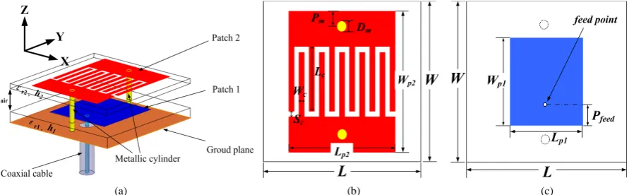
Both of 3D perspective and plane view of the proposed planar electrically small antenna is shown in Figure 1. The new configuration consists of two stacked dielectric substrate isolated by air. There is a rectangle patch on the top of the first substrate with ε =r1 2.65, h1=3 mm and a rectangle patch etched with interdigital capacitor on the top of the second substrate with ε =r2 2.65, h2=0.5 mm, connecting to the ground though two metallic cylinders. In our designs, the planar microstrip patch antenna (MPA) was chose as the driven element. This is mainly due to the advantage of its integrated ground plane and easily to be fixed on other platforms.
According to the near-field resonant parasitic viewpoint, patch 1 is for driven element [see Figure 1(b)], and is immediately fed by 50 Ω coaxial coble; the combination of patch 2 together with the two metallic cylinders [see Figure 1(c)] can be seen as a double-negative shell enclosing on the hemisphere of patch 1. Actually, it can be drawn in Figure 2 that the equivalent model of the whole antenna system. In Figure 2, represents the inherent
[image:2.595.93.539.544.682.2](a) (b) (c)
capacitance of patch antenna, and represents the series capacitance and shunt inductance of the DNG metamate-rials, and depicts the coupled capacitance between the patch and DNG metamaterials. Thus, the resonant fre-quency of the circuit model is approximately
(
)
(
)
2 1 2π c p resp c p p a c p
C C
f
L C C L C C C
+ ≈
+ + (1)
[image:3.595.124.537.262.530.2] [image:3.595.190.440.269.377.2]The HFSS-predicted performance characteristics of this electrically small antenna are given in Figure 3 and
Figure 4. For comparison, the corresponding results for the same sized microstrip patch antenna (MPA) shown in Figure 1(b) are also given.
As is shown in Figure 3(a), the fundamental resonance frequency of this MPA appears at 1316 MHz, with the input impedance value Zin=72.15+ j4.3Ω. This is the well known half wavelength
(
λ0 2)
resonance fre-quency. Not similar to Figure 4(a), one can see from Figure 3(b) that besides the RF frequency 1420 MHz with the impedance value Zin3=514.4−j37.2Ω; there are other two resonance modes inspired at 837 MHz and 299Cp
Lp
Lp
Ca Ra Ca Lp Lp
[image:3.595.88.542.403.530.2]Cp R0 Cc Driven element Parastic element Electrically small antenna
Figure 2. Lumped element circuit for the proposed electrically small antenna.
200 400 600 800 1000 1200 1400 1600 1800 2000 -100 -50 0 50 100 Im pedanc e ( O hm )
Frequency (MHz)
Re (Z11)
Im (Z11)
200 400 600 800 1000 1200 1400 1600 1800 2000 -300 -200 -100 0 100 200 300 400 500
291 294 297 300 303 306 309 -40 -20 0 20 40 60 Im pedanc e (O hm )
Frequency (MHz)
Re (Z11)
Im (Z11)
[image:3.595.197.431.576.692.2](a) (b)
Figure 3. HFSS-predicted input impedance values versus frequency for (a) conventional MPA; (b) Proposed ESA based on DNG metamaterial.
200 400 600 800 1000 1200 1400 1600
-30 -25 -20 -15 -10 -5 0
298 299 300 301 302 -30 -25 -20 -15 -10 -5 0 Frequency (MHz) |S 11 | (d B) conventional MPA ESA based on DNG material
MHz, with their impedance value Zin2=72.5+ j20.9 and Zin1=43.7+ j8.3 respectively. The HFSS-pre- dicted reflection coefficients of the proposed ESA were shown in Figure 4 along with that of the conventional MPA. From Figure 4 it is clear that the proposed ESA based on DNG metamaterial has three resonance fre-quencies, a well impedance matching is obtained at the VHF and UHF.
For studying the radiate mechanism of the proposed ESA, the 3D polar radiation patterns operating at 299 MHz, 837 MHz, and 1420 MHz were shown in Figure 5. At 299 MHz, the maximum radiate direction is at XOZ plane, this can be seen as end-fire omnidirectional antenna; at 837 MHz, the maximum radiate direction is at XOY plane, this can be seen as broadside omnidirectional antenna; at 1420 MHz, the maximum radiate direc-tion is at +Z direcdirec-tion, this can be seen as half wavelength
(
λ0 2)
radiation model, in other words, a conven-tional patch antenna.Since the third resonance frequency showing in Figure 3 and Figure 4 was not a good impedance matching, we prefer to research the first and second resonance frequency which belongs to VHF and UHF respectively.
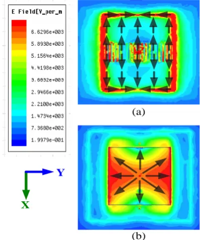
Figure 6 and Figure 7 depict the electric field distributions predicted by HFSS both on the upper and nether plane, and the black arrow expresses the direction of induced current. In Figure 6, the electrical field mainly concentrates at the centre on the upper layer, this demonstrates that the interdigital capacitor is the main contri-butor for electromagnetic wave radiating. The current direction on the two layers indicates that this radiation maybe a linearly polarized model along X direction. In Figure 7, the electrical field concentrates both on the edge of the upper patch and the nether patch. The current distribution is symmetrical with respect to YOZ plane on the upper patch central symmetrical on the nether patch. This makes the antenna like a zeroth-order resonant cavity and radiates a linearly polarized model along Z direction.
Z
X Y
Z
X Y
Z
X Y
(a) (b) (c)
Figure 5. HFSS-predicted 3D polar radiation pattern of proposed ESA operating at (a) 299 MHz, (b) 837 MHz, (c) 1420 MHz.
(a)
(b)
Y
X
3.
Experimental Results of the Proposed Electrically Small Antenna
Figure 8 shows the prototype of the fabricated electrically small antenna. Both driven and parasitic elements were printed on the 100 × 100 mm2 F4B substrate (ε =r 2.65, tanσ =0.001) specified by the design illustrated
in Figure 1. It is a double layer stacked antenna separated by air and fed by a coaxial cable with characteristic impedance equal to 50 Ω on the back ground. Then it was connected to the vector network analyzer (VNA) ca-ble and measured its network characteristics.
The measured reflection coefficient of the proposed antenna is plotted in Figure 9 along with that calculated via full-wave simulation by the HFSS. The measured resonant frequency is about 1% shifts higher than the si-mulated one, which can be contributed to fabrication process and dielectric constant tolerance in a frequency re-gime. The 3 dB fractional bandwidth (FBW3 dB) is 1.5 MHz extended from 301.59 MHz to 303.20 MHz, 19 MHz extended from 832.26 MHz to 851.26 MHz, corresponding to fractional bandwidth of 0.5% and 2.3%, re-spectively. The narrow bandwidth demonstrated that the high quality factor (Q) and strong resonance characte-ristic of the electrically small antenna. Enhanced bandwidth would be obtained by introducing a NIC circuit based on non-Foster element.
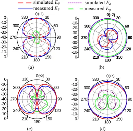
The numerical and experimental radiation patterns of the proposed dual-band antenna operating at 299 MHz and 837 MHz are shown in Figure 10. At 299 MHz, in E-plane [seeing Figure 10(a)] the maximum lies on +Z
(a)
(b)
Y
[image:5.595.212.411.295.534.2]X
Figure 7. HFSS-predicted E-field distribution on (a) the upper layer and (b) nether layer of the proposed ESA operating at 299.6 MHz.
[image:5.595.185.443.574.703.2]
(a) (b)
280 290 300 310 320 700 750 800 850 900 950 1000 -25 -20 -15 -10 -5 0 |S11 | ( d B) simulated measured
[image:6.595.213.412.85.210.2]Frequency (MHz)
Figure 9. Measured and simulated reflection coefficient of the proposed dual-band antenna.
simulated Eθ simulated Eφ
measured Eθ measured Eφ
-40 -30 -20 -10
0 0 30
60 90 120 150 180 210 240 270 300 330 -40 -30 -20 -10 0 (+Z) -40 -30 -20 -10
0 0 30
60 90 120 150 180 210 240 270 300 330 -40 -30 -20 -10 0 (+Z)
(a) (b)
-40 -30 -20 -10
0 0 30
60 90 120 150 180 210 240 270 300 330 -40 -30 -20 -10 0 (+X) -40 -30 -20 -10
0 0 30
60 90 120 150 180 210 240 270 300 330 -40 -30 -20 -10 0 (+X)
(c) (d)
Figure 10. The simulated and measured radiation patterns at 299 MHz in (a) YZ plane, (b) XZ plane; at 837 MHz in (c) YZ plane, (d) XY plane.
direction
(
θ =0o)
and in H-plane [seeing Figure 10(b)] the proposed antenna has an omnidirectional radiation characteristic. At 837 MHz, in E-plane [seeing Figure 10(c)] the maximum lies on +Y direction(
θ =90o)
and in H-plane [seeing Figure 10(d)] the proposed antenna has an approximately omnidirectional radiation charac-teristic. Since the antenna has a none-damaged ground plane, the back lobe can be reasonably decreased when it is fixed on a sufficiently large metal platform.The measured antenna efficiency and peak gain are presented in Figure 11. When operating at VHF, the effi-ciency of the proposed antenna is higher than 70% over the 3-dB bandwidth spectrum with a peak value of 75%; when operating at UHF, the efficiency of the proposed antenna is higher than 95% over the 3-dB bandwidth spectrum with a peak value of 98%. The measured peak gain is 0.2 dBi and 2.8 dBi at 299MHz and 837 MHz respectively.
4. Conclusion
[image:6.595.206.420.249.459.2]280 290 300 310 750 800 850 900 950
0 10 20 30 40 50 60 70 80 90 100
RE Peak Gain
Frequency (GHz)
R
adi
at
ion E
ff
ic
ienc
y (
%
)
-5 -4 -3 -2 -1 0 1 2 3 4 5
P
eak
G
ai
[image:7.595.216.413.82.203.2]n
Figure 11. Measured radiation efficiency and peak gain of the proposed antenna.
compact size and the none-damaged ground configuration of the proposed antenna still demonstrate the potential of applying the antenna to the wireless communication.
References
[1] Chu, L.J. (1948) Physical Limitations of Omnidirectional Antennas. J. Appl. Phys, 19, 1163-1175. http://dx.doi.org/10.1063/1.1715038
[2] Wheeler, H.A. (1947) Fundamental Limitations of Small Antennas. IRE Proc., 35, 1479-1484.
[3] Wheeler, H.A. (1959) The Radiansphere Around a Small Antenna. IRE Proc., 47, 1325-1331. [4] Wheeler, H.A. (1975) Small Antennas. IEEE. Trans. Antennas Propag, AP-23.
[5] Best, S.R. (2005) Low Q Electrically Small Linear and Elliptical Polarized Spherical Dipole Antennas. IEEE. Trans.
Antennas Propag., 53, 1047-1053. http://dx.doi.org/10.1109/TAP.2004.842600
[6] Ziolkowski, R.W., Jin, P. and Lin, C.-C. (2011) Metamaterial-Inspired Engineering of Antennas. Proc. IEEE, 99, 1720-1731. http://dx.doi.org/10.1109/JPROC.2010.2091610
[7] Erentok, A. and Ziolkowski, R.W. (2007) An Efficient Metamaterial-inspired Electrically-Small Antenna. Microw. Opt. Tech. Lett., 49, 1287-1290.
[8] Erentok, A. and Ziolkowski, R.W. (2007) Two-Dimensional Efficient Metamaterial-Inspired Electrically-Small An-tenna. Microw. Opt. Tech. Lett., 49, 1669-1673.
[9] Erentok, A. and Ziolkowski, R.W. (2008) Metamaterial-Inspired Efficient Electrically Small Antennas. IEEE. Trans.
Antennas Propag., 56, 691-707. http://dx.doi.org/10.1109/TAP.2008.916949
[10] Ziolkowski, R.W. (2008) Efficient Electrically Small Antenna Facilitated by a Near-Field Resonant Parasitic. IEEE
Antennas Wireless Propag. Lett., 7, 580-583. http://dx.doi.org/10.1109/LAWP.2008.2000558
[11] Ziolkowski, R.W. (2008) An Efficient, Electrically Small Antenna Designed for VHF and UHF Applications. IEEE
Antennas Wireless Propag. Lett., 7, 217-220. http://dx.doi.org/10.1109/LAWP.2008.921635
[12] Ziolkowski, R.W., Lin, C.-C., Nielsen, J.A., Tanielian, M.H. and Holloway, C.L. (2009) Design and Experimental Ve-rification of a 3D Magnetic EZ Antenna at 300 MHz. IEEE Antennas Wireless Propag. Lett., 8, 989-993.
http://dx.doi.org/10.1109/LAWP.2009.2029708
[13] Ziolkowski, R.W., Jin, P., Nielsen, J.A., Tanielian, M.H. and Holloway, C.L. (2009) Experimental Verification of Z Antennas at UHF Frequencies. IEEE Antennas Wireless Propag. Lett., 8, 1329-1333.
http://dx.doi.org/10.1109/LAWP.2009.2038180
[14] Jin, P. and Ziolkowski, R.W. (2009) Low Q, Electrically Small, Efficient Near-Field esonant Parasitic Antennas. IEEE.
Trans. Antennas Propag., 57, 2548-2563. http://dx.doi.org/10.1109/TAP.2009.2027162
[15] Jin, P. and Ziolkowski, R.W. (2010) Broadband, Efficient, Electrically Small Metamaterial-Inspired Antennas Facili-tated by Active Near-Field Resonant Parasitic Elements. IEEE. Trans. Antennas Propag., 58, 318-327.
http://dx.doi.org/10.1109/TAP.2009.2037708
[16] Lin, C.-C., Ziolkowski, R.W., Nielsen, J.A., Tanielian, M.H. and Holloway, C.L. (2010) An Efficient, Low Profile, Electrically Small, Three-Dimensional, Very High Frequency Magnetic EZ Antenna. Appl. Phys. Lett., 96, Article ID: 104102. http://dx.doi.org/10.1063/1.3357430
[17] Lin, C.-C., Jin, P., Ziolkowski, R.W. (2011) Multi-Functional, Magnetically-Coupled, Electrically Small, Near-Field Resonant Parasitic Wire Antennas. IEEE. Trans. Antennas Propag., 59, 691-707.
Field Resonant Parasitic Antennas. IEEE. Trans. Antennas Propag., 59, 1446-1459.
[19] Tang, M.-C. and Ziolkowski, R.W. (2013) Efficient, High Directivity, Large Front-to-Back-Ratio, Electrically Small, Near-Field-Resonant-Parasitic Antenna. IEEE Access, 1, 16-28.
http://dx.doi.org/10.1109/ACCESS.2013.2259134
[20] Zhu, N. and Ziolkowski, R.W. (2012) Broad-Bandwidth, Electrically Small Antenna Augmented With an Internal Non-Foster Element. IEEE Antennas Wireless Propag. Lett., 11, 1116-1120.
http://dx.doi.org/10.1109/LAWP.2012.2219572
[21] Jin, P., Lin, C.-C. and Ziolkowski, R.W. (2012) Multifunctional, Electrically Small, Planar Near-Field Resonant Para-sitic Antennas. IEEE Antennas Wireless Propag. Lett., 11, 200-204.
http://dx.doi.org/10.1109/LAWP.2012.2187322
[22] Jin, P. and Ziolkowski, R.W. (2012) High-Directivity, Electrically Small, Low-Profile Near-Field Resonant Parasitic Antennas. IEEE Antennas Wireless Propag. Lett., 11, 305-309. http://dx.doi.org/10.1109/LAWP.2012.2190030 [23] Tang, M.-C., Zhu, N. and Ziolkowski, R.W. (2013) Augmenting a Modified Egyptian Axe Dipole Antenna With
Non-Foster Elements to Enlarge Its Directivity Bandwidth. IEEE Antennas Wireless Propag. Lett., 12, 421-424. http://dx.doi.org/10.1109/LAWP.2013.2254103
[24] Zhu, N. and Ziolkowski, R.W. (2012) Design and Measurements of an Electrically Small, Broad Bandwidth, Non- Foster Circuit-Augmented Protractor Antenna. Appl. Phys. Lett., 101, Article ID: 024107.