Engineering Postgraduate Conference (EPC) 2008
GATE LENGTH EFFECT ON NMOS ELECTRICAL CHARACTERISTICS USING TCAD TOOLS
N. Osman and R. Sanudin
Faculty of Electrical and Electronic Engineering Universiti Tun Hussein Onn Malaysia, Malaysia.
ABSTRACT
The concept of device scaling in silicon transistor has consistently resulted in better device density and performance. In conventional MOSFETs, control of Ioff for scaled devices requires very thin gate dielectrics and high doping concentrations. The industry roadmap for CMOS technology predicts physical limitations as well as practical technological will become barriers to continuous scaling. As the downscale of CMOS technology approaches physical limitations, the need arises for alternative device structures. NMOS traditionally has been the dominant MOS technology. Relative to CMOS, NMOS shows higher speed, higher-power technology with lower cost and higher functional density.
Keyword: silicon transistor; NMOS; gate length
INTRODUCTION
Silicon CMOS has emerged as the predominant technology in semiconductor industry (Song, 2000; Jurczak, 2001; Caillat, 1999). It has been continuously scaled down in terms of size but higher capacity and complexity (Risch, 1996; Choi, 2002). As device size as came into nanoscale regime, therefore novel structure is needed. Conventional MOSFET also suffers from higher leakage current, short channel effect and doping uniformity (Saad, 2007; Jayanarayanan, 2006; Huang, 2004). NMOS structure is proposed in order to reduce the leakage current and offer better handling of short channel effect.
EXPERIMENTAL PROCEDURE
MOSFETs operate in such a way that the current from the source to drain is carried by electrons (NMOS), by holes (PMOS) or by both electrons and holes in the case of complementary MOSFET (CMOS). Figure 1 shows a schematic of an NMOS device with p-type substrate. A voltage is applied to the gate that ‘inverts’ the polarity of the carriers and produces electrons near the oxide-semiconductor interface. The gate length is one of the most critical parameters controlling device performance. The body or substrate of a MOSFET can also be contacted and a bias applied to it.
FIGURE 1 The side and top view of n-type MOSFET structure
Sentaurus includes a comprehensive suite of core TCAD products for multidimensional process, device, and system simulations, embedded into a powerful user interface. The comprehensive Sentaurus TCAD suite bridges the needs of development and manufacturing engineers by improving semiconductor process control in manufacturing. In this paper, Sentaurus TCAD is used extensively right from the start of the device modeling, construct the device structure, determining the process flow and finally plotting the device output characteristic. Upon plotting the device characteristic, all process parameters have been established. Figure 2 depicts the process flow in simulating the NMOS transistor in the Sentaurus TCAD.
RESULT AND DISCUSSION
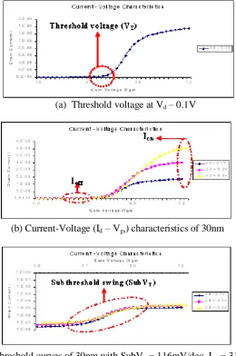
Figure 3, 4 and 5 illustrate the current-voltage (Id-Vgs) characteristics and subthreshold curves for NMOS device of channel length Lg at 30nm, 50nm and 100nm respectively with uniform boron doping concentration of 1012 cm-3 to 1020 cm-3. The measured threshold voltage is shown in Figure 3(a). In Figure 3(b), three curves represent simulated output at Vds = 0.1V, 0.2V and 0.3V separately for gate length 30nm. In Figure 3(c), Vgs sweeps from 0V to 1.2V which produced Ion – Ioff current ratio, subthreshold swing and leakage current. All these characteristics are the same for the gate length at 50nm and 100nm respectively.
(a) Threshold voltage at Vd – 0.1V
(b) Current-Voltage (Id – Vgs) characteristics of 30nm
(c) Subthreshold curves of 30nm with SubVT = 116mV/dec, Ioff = 31nA/µm and Ion = 14µA/µm at Vds = 0.1V
For comparison between 30nm with 50nm and 100nm gate length as shown in Figure 4 and 5, the results obtained show a good off-state leakage current Ioff of 0.61pA/µm and drive current Ion of 7µA/µm at 100nm gate length because the Ioff is lower than Ion current. When gate voltage decreases, drive current will be higher because the gate length expands from 30nm to 100nm and this will provide more current to pass through it compared with gate length of 30nm and 50nm.
(a) Current-Voltage (Id – Vgs) characteristics of 50nm
[image:4.595.146.447.223.515.2](b) Subthreshold curves of 50nm with SubVT = 85mV/dec, Ioff = 34pA/µm and Ion = 12µA/µm
FIGURE 4 I-V characteristics of NMOS with Lg = 50nm and VT = 0.32V taken at Vds = 0.1V, 0.2V and 0.3V
Current - Voltage Characteristics 1,E-13 1,E-11 1,E-09 1,E-07 1,E-05 1,E-03 1,E-01 1,E+01
0,0 0,1 0,6 1,2
Gate Voltage (Vgs)
D ra in C urr e nt ( Id)
Vd = 0.1V
Vd = 0.2V Vd = 0.3V
[image:5.595.161.436.127.267.2](b) Subthreshold curves of 100nm with SubVT = 81mV/dec, Ioff = 0.61pA/µm and Ion = 7µA/µm
FIGURE 5 I-V characteristics of NMOS with Lg = 100nm and VT = 0.41V taken at Vds = 0.1V, 0.2V and 0.3V
CONCLUSION
The design and simulation of gate length effect on NMOS electrical characteristics based on the structured reported in has been successfully done using commercial 3D Sentaurus TCAD tools. By employing the inversion layer mobility model from Lombardi combined with SRH (Shockley-Read-Hall Recombination), a detailed investigation on the n-channel MOSFET performance was done. With a good drive current Ion of 7µA/µm and a low off-state leakage current Ioff of 0.61pA/µm was explicitly shown for 100nm NMOS. Besides that, the subthreshold characteristics also highlighted a reasonably well-controlled SCE with subthreshold swing SubVT = 81mV/decade and threshold voltage VT = 0.41V. Efforts to reduce the sheet resistance still further are continuing, with the aim of further improving current drive.
REFERENCES
Caillat C., Deleonibus S., Guegan G., Tedesco S., Dal’zotto B., 1999. 65nm physical gate length NMOSFETs with heavy ion implanted pockets and high reliable 2 nm-thick gate oxide for 1.5 V operation. Symp. VLSI Technol. Dig. 89
Huang H., Chen S., Chang Y., Line H., Lin W. 2004. TCAD Simulation of Using Pocket Implant In 50nm N-Mosfets, National Taipei University of Technology.
Jayanarayanan S. K., Dey S., Donnelly J. P., Benerjee S. K. 2006. A Novel 50nm Vertical MOSFET with a Dielectric Pocket, Solid-State Elecronics.50, 897-900.
Jurczak M., Skotnicki T., Gwoziecki R., Paoli M., Tormen B. 2001. Dielectric Pockets – A New Concept of the Junctions for Deca-Nanometric CMOS Devices. IEEE Trans. Electron Devices.48. 1770 – 1774.
Risch L., Krautschneider W. H., Hofmann F., Schafer H., Aeugle T. and Rosner W., 1996. Vertical MOS Transistors with 70 nm Channel Length, IEEE Trans. on Electron Devices, 43(9), 200 – 204.
Ruangphanit A., Harnsoongnoen S., Muanghlua R., Phongphanchantra N. and
Poyai A. 2006. Drain Induced Barrier Lowering (DIBL) Effect in
Submicrometer NMOS Devices. Khonkaen University.
Saad I., Ismail R. 2007. Numerical Simulation Characterization of 50nm MOSFET incorporating Dielectric Pocket (DP-MOSFET), Regional Symposium of Microelctronics.