052
PROCESS AND DEVICE SIMULATION OF 80NM CMOS INVERTER USING
SENTAURUS SYNOPSYS TCAD
Muhammad Suhaimi Sulong, Asyiatul Asyikin Jamry, Siti Maryaton Shuadah Shuib, Rahmat Sanudin, Marlia Morsin, Mohd Zainizan Sahdan
Microelectronics & Nanotechnology-Shamsuddin Research Centre, Faculty of Electrical and Electronics Engineering,
University Tun Hussein Onn Malaysia, 86400 Parit Raja, Johor, Malaysia. Email: [email protected]
ABSTRACT
Nowadays, the simple manufacturing process of CMOS transistor is widely used in digital design implementation. Using the latest technology in fabrication, the sizes of semiconductor devices are ever shrinking toward the nanotechnology. This paper presents the development of 80nm gate length of CMOS inverter with modification of the theoretical values in order to obtained more accurate process parameters. Simulation of the process and device fabrication using Sentaurus Synopsys TCAD has been carried out and the electrical characteristics of the device were studied and analyzed. The result of the study indicates that the operational of CMOS inverter was at VT = 0.499V, Ioff =79.08pA/m and IDSAT = 429.3A/m for NMOS device. The values were then compared with 90nm CMOS inverter. The study also found that the leakage current of 80nm CMOS transistor is almost twice higher than 90nm CMOS transistor.
Keywords: CMOS, gate length, Sentaurus Synopsys TCAD, nanotechnology.
INTRODUCTION
Microelectronics has evolved tremendously in the last century [1]. Nowadays, the simple manufacturing process of CMOS transistor is widely used in digital design implementation. Using the latest technology in fabrication, the sizes of semiconductor devices are ever shrinking toward the nanotechnology. The MOS transistor is extensively used in digital circuits because it is a very good and efficient switch. By designing the MOS transistor in smaller gate length size, automatically the better the transistor in speed. This strategy has been driven by the increased performance that smaller devices make possible and the increased functionality that larger chips provided. Currently, NMOS and PMOS transistor is the most important device to create the CMOS circuit.
CMOS has been used widely in electronic device, which is many CMOS circuit has been designed such as inverter, logic gate, multiplexer, memory and etc. CMOS is under MOSFET family and it provides both NMOS and PMOS on the same chip. The main reasons for the success of CMOS are low power consumption and good noise immunity [2]. Others are low supply voltage, low leakage current, high speed performance, less transit time and etc [3]. In fact, currently only CMOS technology is used in advanced integrated-circuit (IC).
PROCESS FLOW
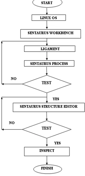
The process flow for 80nm CMOS device was developed using Sentaurus Synopsys TCAD software with several stages as illustrated in Figure 1. The simulation starts with the bare wafer and finishes with device structure. Implantation, diffusion, etching, growth, and deposition process are simulated on a microscopic level.
[image:2.595.227.364.157.439.2]
Figure 1: Process flow of Sentaurus Synopsys TCAD
The process flow in this project represents a generic 80 nm technology node and it follows the common CMOS process flow. The major process steps are [4]:
1. Well definition. 2. Gate oxide growth. 3. Polysilicon gate definition. 4. Polysilicon gate reoxidation. 5. Offset spacer creation. 6. Halo implant.
7. Source–drain extension implants. 8. First spike anneal.
9. Spacer creation. 10. Source–drain implants. 11. Second spike anneal. 12. Metallization.
The process start with boron-doped p-type silicon as a bare wafer then an oxide layer are grown, followed by applied of photoresist, PR developed, oxide etched, PR removed, phosphorus diffused, field oxide grown, PR applied, PR developed against, oxide etched, PR stripped, PR removed, aluminium film deposited, PR applied against, PR developed and aluminium interconnect etching (metallization). After the final PR stripping, all the NMOS fabrication steps are completed.
Offset-spacer is to define the n and p diffusion. The process source-drain extension implants, first and second spike anneal in this project were for defined the contact holes which is a thin layer of CVD oxide is deposited over the entire wafer to pattern the contact holes. Etching opens the holes. Last process before run this recipe was metallization. A thin layer of aluminium was evaporated or sputtered onto the wafer used to pattern the interconnection.
.
RESULTS AND DISCUSSIONS
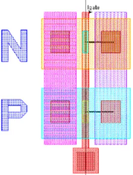
The model of 80nm NMOS and PMOS transistor in two dimensions (2D) as shown in Figure 2(a) and 1(b) respectively was the result from the process simulation in the Tecplot SV. Both devices were defined from CMOS inverter via Ligament Layout Editor as shown in Figure 3.
(a) (b)
[image:3.595.232.366.451.627.2]Figure 2: a) 80nm NMOS transistor, b) 80nm PMOS transistor
Figure 3: An 80nm CMOS transistor with a parameterized layout
Referring to Figure 3, the two horizontal black lines show the cut lines that define the 2D areas for the NMOS and PMOS devices. The vertical line defines the parameterization; the layout is stretched as a function of the parameter gate length (lgate) [4].
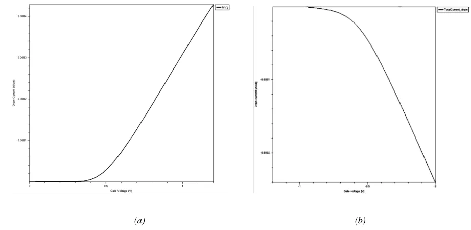
(VD) of the device and monitoring the drain current. A constant voltage is applied to the gate (VG) during each sweep, and a group of (ID-VD) data curves can be acquired by varying the gate voltage between sweeps. A bias voltage can also be applied to the substrate contact (VB) and the source is grounded [3].
[image:4.595.84.512.139.343.2]
(a) (b)
Figure 4: ID-VD characteristics of a) NMOS and b) PMOS transistor
(a) (b)
Figure 5: ID-VG characteristics of a) NMOS and b) PMOS transistor
[image:4.595.62.523.389.614.2]Meanwhile, an off-state leakage current (Ioff) of 80nm CMOS transistor is almost twice higher than 90nm CMOS transistor. This shows the smaller gate length of NMOS transistor, the higher leakage current occurred. An ideal MOS transistor only has current flow when it is “on”; when the channel is “off” there was no current. This means that the transistor should consume no power if it is “off”. Unfortunately, MOS transistors are not ideal and, as they get smaller, they get less ideal.
Table 1: The comparison between 80nm and 90nm CMOS inverter
Condition 90nm CMOS inverter 80nm CMOS inverter
Type NMOS PMOS NMOS PMOS
VT 0.518 -0.526 0.499 -0.491
IDSAT 4.008e-04 2.154e-04 4.293e-04 2.400e-04
Ioff 4.880e-11 1.023e-10 7.908e-11 2.361e-10
The value of VT (threshold voltage) is the voltage required for MOS transistor device to be operated. The VT value obtained for 80nm NMOS and PMOS were 0.499V and -0.491V respectively while for 90nm gate length was 0.518V and -0.526V as shown in Table 1.
VT (the threshold voltage) for a MOS transistor can be defined as the voltage applied between the gate and the source of a MOS device below which the drain-to-source current IDS “effectively” drops to zero [5]. It can be seen that the percentage speed between 90nm and 80nm gate length for NMOS and PMOS transistor was about 3.63% and 6.56%. These are the best value that we have reported. It can be seen that the operation of NMOS transistor is two times faster than PMOS transistor although their size of physical gate length is 80nm. It is because effective mass of hole is greater than electron which means electron have high mobility than hole [6]. A MOS transistor is called a majority carrier device, in which the current in a conducting channel (the region immediately under the gate) between the source and the drain is modulated by a voltage applied to the gate. The majority carriers of an NMOS transistor are the electrons while for PMOS transistor is a holes [7].
Current cannot flow from the drain to the source unless VGS is greater that VT (device not operated, cutoff region). When the applied VGS exceed a critical value, the oxide-layer field begins to draw electrons into the substrate region. It will conducted inversion layer to transfer the electron from the source to drain. ID will flow and device start operated when VGS increase with conductivity of the inversion layer channel. Note that, the inversion layer just at the surface of the substrate (along the gate length) [7]. This shows that the shorter gate length helps the transfer of electron more strongly from source to drain. This clarify by reduction in gate length provides a shorter transit time (during transferred electron along inversion layer) and hence a faster device to operated. In addition, the size is reduced due to smaller gate length.
[image:5.595.80.524.526.679.2]
(a) (b) (c)
Figure 6: I-V characteristics of 80nm CMOS transistor
CONCLUSIONS
The simulation of process and device development for gate length of 80nm CMOS inverter has been achieved. It has been demonstrated that the percentage speed between 90nm and 80nm gate length for NMOS and PMOS transistor was about 3.63% and 6.56% and the percentage of increasing IDSAT for NMOS and PMOS transistor was about 7.1% and 11.4%. It was observed that the 80nm NMOS device has lower VT and higher IDSAT and Ioff than 90nm device. Further study will look onto lower technology node with standard CMOS process flow.
ACKNOWLEDGEMENT
The author would like thank to Ministry of Higher Education for the grant support in Fundamental Research Grant Scheme (FRGS), Vot No. 0400.
REFERENCES
[1] Shekhar Borkar (2006) Electronics Beyond Nano-Scale CMOS. DAC2006, San Francisco, California, U.S.A.
[2] Hong Xiao (2001) Introduction to Semiconductor Manufacturing Technology. New Jersey: Prentice Hall.
[3] Sulong, M.S., Ahmad, I., Lim, T.F., and Yeap, K.H. (2007) Characterization of 130nm CMOS Device using CVIV and Focused Ion Beam. Journal of Science and Technology, pp. 37-46.
[4] Synopsys (2005) Sentaurus Technology Template: CMOS Processing. Copyright © 2005 Synopsys, Inc.
[5] Uda Hashim (2001) N/P Chanel MOSFET Fabrication. Unpublished lecture notes, UMP.
[6] Badcock, S.G., O’Neil, A. G. and Chester, E.G. (2002) Device and Circuit Performance of SiGe/Si MOSFETs. Solid-State Electronics 46, pp. 1925-1932.
[7] Wong, B.P., Mittal, A., Yu Cao, Starr, G.W. (2004) Nano-CMOS Circuit and Physical Design. John Wiley & Sons Inc.
[8] Fujinaga, M., Itoh, S., Mochiduki, M., Uchida, T., Ishikawa, H., Takenaka, M., Park, C.J., Asada, S., Shinzawa, T., Namekata, J., Wakahara, S., and Wada, T. (2006) 3-D Process Simulation of CMOS Inverter Based on Selete 65nm Full Process. Proceedings, Technical Report, IEEE.
[9] Micheal Aquilino (2004) Advancing RIT to Submicron Technology: Design and Fabrication of 0.5µm N