N A N O I D E A
Open Access
Patterned Si thin film electrodes for enhancing
structural stability
Gyu-bong Cho, Jung-pil Noh, Ho-jin Sung, Sang-hun Lee, Yeon-min Im, Hyo-jun Ahn and Ki-won Kim
*Abstract
A patterned film (electrode) with lozenge-shaped Si tiles could be successfully fabricated by masking with an expanded metal foil during film deposition. Its electrochemical properties and structural stability during the charge-discharge process were examined and compared with those of a continuous (conventional) film electrode. The patterned electrode exhibited a remarkably improved cycleability (75% capacity retention after 120 cycles) and an enhanced structural stability compared to the continuous electrode. The good electrochemical performance of the patterned electrode was attributed to the space between Si tiles that acted as a buffer against the volume change of the Si electrode.
Keywords:patterned electrode, silicon film, stress, anode
Introduction
The secondary Li-ion batteries with a high energy den-sity have gained attention from wide-range applications of power source for the portable electronics, electric vehicle, and electric storage reservoir. In order to increase the energy density in the limited battery volume, the volume of the cathodic electrode having Li sources should be increased, whereas that of the anodic electrode has to be decreased, that is, anode materials with high theoretical capacity are needed to store the large amount of Li ions.
For the anodic materials, some of the candidates are Si, Sn, Al, Ge, and compounds including these elements [1,2]. Si has a much higher specific energy (4,200 mAh/ g for Li4.4Si) than commercial graphite (372 mAh/g for LiC6). However, there is a severe practical problem in the application of Si electrodes, i.e., when Si is used as an anode material for Li-ion batteries, a large volume expansion/shrinkage occurs during the charge-discharge (lithiation-delithiation) process. The volume change of Si (310%) causes surface cracking and pulverization of the Si film and leads to a rapid capacity fade during initial cycles. The poor electrochemical performances are ultimately caused by repetitive mechanical stress
accompanied by large volume changes [3]. Until now, many attempts have been made to prolong the cycle life of Si film electrodes [4-9]. Most researches focused on enhancing the adhesion between the Si film and a cur-rent collector (substrate) because the amount of Li sto-rage was limited and the generation of stress was restrained by the enhanced adhesion.
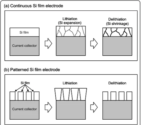
In this work, as a new approach to overcome the pro-blem, space was given to the Si film like a patterned Si film. The Si film including the space is expected to accumulate the stress generated by the volume change during the charge-discharge process. Figure 1 shows schematic diagrams of the estimated changes in Si elec-trodes with different film types of continuous (conven-tional) and patterned films during the lithiation-delithiation process. For a continuous Si film, the stress generated by the volume expansion during lithiation generates cracks in the Si film or the interface between the film and substrate, and the volume shrinkage during delithiation causes severe surface cracking [3,10]. In contrast, for a patterned Si film, the space between the patterned Si film units makes room to expand the volume of Si during the lithiation process and to mini-mize the stress generated in the Si film electrode. These characteristics of the patterned Si film are expected to minimize the structural damage of the Si film and improve the electrochemical reversibility of the electrode.
* Correspondence: kiwonkim@gnu.ac.kr
School of Materials Science and Engineering, Research Institute for Green Energy Convergence Technology, Gyeongsang National University, Gazwadong 900, Jinju, Gyeongnam 660-701, Korea
In this article, the electrochemical properties of the continuous and patterned Si film electrodes are exam-ined, and the improved cycle performance of the pat-terned electrode is discussed by observing the surface morphologies after 10 cycles.
Experimental details
A patterned Si film was fabricated by using an expanded metal foil (stainless steel) with lozenge-patterned holes (THANKS-METAL, Japan) as a mask. A continuous (conventional) Si film electrode was also fabricated for comparison. The Si films were deposited on a Cu foil substrate using DC magnetron sputtering systems. Prior to the deposition, the Cu substrate was ultrasonically cleaned and annealed in vacuum-sealed ampules at 573 K for 30 min to remove the residual impurity gases at the surface. The films were grown in a vacuum chamber under a pressure of 5 × 10⁻³Torr in argon atmosphere. A cross-sectional analysis was performed to measure thick-ness of the film with an alpha-step profiler. The thickthick-ness of the Si film fabricated in this study was 350 nm.
Crystallinity and surface morphology of the two Si films were investigated by means of transmission elec-tron microscopy [TEM], X-ray diffraction [XRD], and field emission scanning electron microscopy. Although the stress generated during the electrochemical test was indirectly traced by analyzing the broadness of the sub-strate peaks, a clear distinction before and after the test was difficult.
Electrochemical measurements were preformed in CR2032 coin cells with the different Si film electrodes.
A metal lithium foil was used as a counter electrode. Electrolyte was made from 1 M LiPF6 in a 1:1 (v/v) mix-ture of ethylene carbonate and dimethyl carbonate. The separator used was a porous polypropylene (Celgard 2400; Celgard, Charlotte, NC, USA). Galvanostatic charge-discharge half-cell tests were performed at a cur-rent density of 2,100 mA/g (0.5C-rate) at ambient tem-perature. The test was conducted between the initial OCV and 0.01 V versus Li/Li+, then between 0.01 and 1.2 V after the first cycle. Charge-discharge measure-ments were performed with a constant current. For the calculation of capacity, the mass of the Si electrode is derived from its density, 2.33 g/cm2, assuming the crys-talline structure.
Results and discussion
Scanning electron microscopy [SEM] photographs of the continuous and patterned Si films are shown in Figures 2a and 2c, respectively. For the two Si films, energy dis-persive spectrometry [EDS] mapping images of the Si element are also given in Figures 2b and 2d, showing the difference in distribution of Si. Tile-like Si films with the lozenge shape observed in the patterned Si film are arranged with the regular space between them. From Figure 2c, the width [w] and height [h] of the Si tile are about 700μm and 270μm, respectively, and the Si-deposited area ratio of the patterned film is about 83% for the continuous film. These results demonstrate that a well-patterned Si film (electrode) can be simply fabricated by masking with an expanded metal foil.
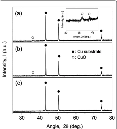
Figure 3 shows XRD profiles of continuous and pat-terned Si films. For comparison, the XRD result of a Cu substrate is presented in Figure 3a. No peaks related to Si can be found for the two films (Figures 3b, c) though the highest-intensity peak of crystalline Si appears at 2θ = 28°. This indicates that the Si films fabricated in this work are amorphous. In the previous work, TEM results of the Si film with the same thickness revealed a hollow pattern corresponding to a disordered structure [9]. The amorphous Si is known to be an effective structure to obtain better electrochemical properties than the crystal-line Si [7,11].
However, weak peaks of CuO are observed in Figures 3a and 3b. The formation of CuO can be confirmed in the inset of Figure 3a where peaks corresponds to (111) and (200) planes of CuO (JCPDS 80-1719), respectively. The CuO layer seems to form on the surface of the Cu substrate during the annealing process. The intensity of CuO peaks decreases at the patterned Si film and almost disappears at the continuous Si film. This is acceptable because the Si-covered area for the continuous film is wider than that for the patterned film.
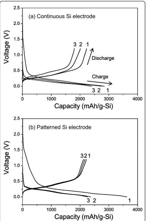
Charge-discharge behaviors of cells with continuous and patterned films (electrodes) are compared in Figure 4.
Si film
Current collector
Delithiation (Si shrinkage) Lithiation
(a) Continuous Si film electrode
Si film
Current collector
Delithiation Lithiation
(b) Patterned Si film electrode
(Si expansion)
Si film
Current collector
Delithiation (Si shrinkage) Lithiation
(a) Continuous Si film electrode
Si film
Current collector
Delithiation Lithiation
(b) Patterned Si film electrode
[image:2.595.56.292.89.298.2](Si expansion)
The cell test was performed at the same current density of 2,100 mA/g corresponding to 0.5C-rate. Notice that vol-tage decreases during the charge process (lithiation). Two voltage plateaus can be observed in each cell, and this is a typical charge-discharge behavior of amorphous Si [12].
At the first cycle, 2,890 mAh/g of charge capacity and 2,200 mAh/g of discharge capacity were obtained from the continuous electrode (Figure 4a), and 3,620 mAh/g and 2,200 mAh/g capacities were obtained from the pat-terned electrode (Figure 4b). The relatively high charge capacity of the patterned electrode is mainly related to an electrochemical reaction between Li and Cu oxide layers partially exposed on the surface. It had been already reported that the reaction occurred at a voltage range of 1.7 V to 1.0 V and then formed LixCuO [13]. In addition to this, another reason is the solid electrolyte interphase formation that is sensitive to the surface morphology of the electrode because the patterned trode has a wider surface area than the continuous elec-trode [6]. These reaction products lead to the capacity loss at the first cycle, and thus a low coulombic effi-ciency ((discharge capacity/charge capacity) × 100(%)) of 60% was obtained at the first cycle as shown in Figure 4b. However, the patterned electrode exhibits higher efficiencies than those of the continuous electrode which were obtained after the first cycle.
The cycle performances of cells with the continuous and patterned Si electrodes are shown in Figure 5. The charge capacity of the continuous electrode has rapidly decreased within the second cycle. On the other hand, it is noticeable that the patterned Si electrode exhibits a high capacity retention (75% for the second cycle) even until 120 cycles. It is considered that the improved cycle performance of the patterned Si electrode is associated with the stress dispersion in the Si film electrode during the charge-discharge process.
(c)
(d)
500 μm 500 μm
Si
(a)
(b)
500 μm 500 μm
Si
W h
[image:3.595.57.540.87.328.2]W h
Figure 2SEM photographs and EDS mapping images of Si film electrodes. (a,b) continuous film and (c,d) patterned film.
30 40 50 60 70 80
(a)
(b)
(c)
Angle, 2T(deg.)
In
te
nsi
ty
, I
(
a.u
.)
30 35 40
Inte
nsity, I(a.u
.)
Angle, 2T(deg.)
: Cu substrate : CuO
30 40 50 60 70 80
(a)
(b)
(c)
Angle, 2T(deg.)
In
te
nsi
ty
, I
(
a.u
.)
30 35 40
Inte
nsity, I(a.u
.)
Angle, 2T(deg.)
: Cu substrate : CuO : Cu substrate : CuO
[image:3.595.58.291.436.692.2]Figure 6 shows surface morphologies of the continu-ous and patterned Si electrodes after 10 cycles. The Si film with severe cracks was partially detached from the substrate in the continuous electrode. Such damage of the film electrodes results from the compressive and tensile stress generated by the insertion and extraction of Li [3]. In contrast, Si tiles with the regular space still remained without the severe damage shown in the con-tinuous electrode. It suggests that the stress generated in the continuous Si electrode is larger than that in the patterned electrode.
However, it can be found that the size of the Si tile was slightly increased after cycling (Figure 2b and 6b),
0 1000 2000 3000 4000 0.0
0.5 1.0 1.5 2.0 2.5
Capacity (mAh/g-Si)
Vo
lta
ge (
V
)
1 3 2
0 1000 2000 3000 4000 0.0
0.5 1.0 1.5 2.0 2.5
Capacity (mAh/g-Si)
Voltage (V)
1 3 2
1 3 2
1 32
Charge Discharge
0 1000 2000 3000 4000 0.0
0.5 1.0 1.5 2.0 2.5
Capacity (mAh/g-Si)
Volt
age (V)
1 3 2
0 1000 2000 3000 4000 0.0
0.5 1.0 1.5 2.0 2.5
Capacity (mAh/g-Si)
Voltage (V)
1 3 2
1 3 2
1 32
Charge Discharge (a) Continuous Si electrode
[image:4.595.57.292.88.442.2](b) Patterned Si electrode
Figure 4 Initial charge-discharge curves of cells with (a) continuous Si electrode and (b) patterned Si electrode. Cycle numbers are described at the top and bottom of the curves.
0 20 40 60 80 100 120
0 1000 2000 3000 4000
Cycle number (n)
C
apacity
(mAh
/g-S
i) : Continuous Si electrode: Patterned Si electrode
0 20 40 60 80 100 120
0 1000 2000 3000 4000
Cycle number (n)
C
apacity
(mAh
/g-S
[image:4.595.305.539.89.264.2]i) : Continuous Si electrode: Patterned Si electrode
Figure 5Charge capacity vs. cycle number curves of cells with continuous and patterned Si electrodes. The open circle denotes the continuous Si electrode, while the closed circle denotes the patterned Si electrode.
Si
(b)
(a)
500
μ
m
500
μ
m
[image:4.595.57.540.506.668.2]500 μm
and relatively small cracks were generated in the pat-terned electrode. Unfortunately, these results indicate that the volume change of Si was completely not rever-sible during the repeated cycling. Therefore, it is con-cluded that the space between tiles in the patterned Si electrode buffers the volume change of Si during the charge-discharge process and partially disperses the stress generated in the Si electrode. In the next work, it is expected that electrochemical properties of the pat-terned electrode fabricated on a substrate without an oxide layer will be highly improved because the adhe-sion between a film and a substrate will be enhanced by the surface treatment of the substrate. Because of this, the study on a surface-etched substrate is in progress.
Conclusions
A patterned Si film (electrode) with lozenge-shaped tiles could be successfully fabricated by masking with an expanded metal foil, and its electrochemical properties were compared with those of a continuous (conven-tional) film electrode. The patterned electrode exhibits a remarkably improved cycleability compared to the con-tinuous electrode with 75% capacity retention after 120 cycles. After 10 cycles, the continuous Si film with severe cracks was partially detached from the substrate, whereas Si tiles in the patterned film still remained without severe damage. The good electrochemical per-formances of the patterned electrode were attributed to the space between Si tiles that acted as a buffer against the volume change of Si.
Acknowledgements
This research was supported by the Pioneer Research Center for Nano-morphic Biological Energy Conversion and Storage. This research was partially supported by the Basic Science Research Program through the National Research Foundation of Korea (NRF) funded by the Ministry of Education, Science and Technology (2011-0024767).
Authors’contributions
GBC, JPN, and YMI participated in the design of the study and carried out the experimental works on SEM, XRD, cycle testing etc. HJS participated in the cycle testing. HJA analyzed the electrochemical data. KWK participated in the drafting of the manuscript. All authors read and approved the final manuscript.
Competing interests
The authors declare that they have no competing interests.
Received: 27 September 2011 Accepted: 5 January 2012 Published: 5 January 2012
References
1. Tirado JL:Inorganic materials for the negative electrode of lithium-ion batteries: state-of-the-art and future prospects.Mater Sci Eng R2003, 40:103.
2. Winter M, Besenhard JO:Electrochemical lithiation of tin and tin-based intermetallics and composites.Electrochim Acta1999,45:31.
3. Lee SJ, Lee JK, Chung SH, Lee HY, Lee SM, Baik HK:Stress effect on cycle properties of the silicon thin-film anode.J Power Sources2001,97-98:191.
4. Ohara S, Suzuki J, Sekine K, Takamura T:Li insertion/extraction reaction at a Si film evaporated on a Ni foil.J Power Sources2003,119-121:591. 5. Kim JB, Jun BS, Lee SM:Improvement of capacity and cyclability of Fe/Si
multilayer thin film anodes for lithium rechargeable batteries.Electrochim Acta2005,50:3390.
6. Park MS, Wang GX, Liu HK, Dou SX:Electrochemical properties of Si thin film prepared by pulsed laser deposition for lithium ion micro-batteries.
Electrochim Acta2006,51:5246.
7. Bourderau S, Brousse T, Schleich DM:Amorphous silicon as a possible anode material for Li-ion batteries.J Power Sources1999,81-82:233. 8. Zhang T, Fu LJ, Takeuchi H, Suzuki J, Sekine K, Takamura T, Wu YP:Studies
of the structure of vacuum deposited silicon films on metal substrates as anode materials for Li-ion batteries.J Power Sources2006,159:349. 9. Cho GB, Song MG, Bae SH, Kim JK, Choi YJ, Ahn HJ, Ahn JH, Cho KK,
Kim KW:Surface-modified Si thin film electrode for Li ion batteries (LiFePO4/Si) by cluster-structured Ni under layer.J Power Sources2009,
189:738.
10. Cho GB, Cho KK, Kim KW:Effects of Ni film thickness on the structural stability of Si/Ni/Cu film electrodes.Mater Lett2006,60:90.
11. Jung HJ, Park M, Han SH, Lim H, Joo SK:Amorphous silicon thin-film negative electrode prepared by low pressure chemical vapor deposition for lithium-ion batteries.Solod State Commun2003,125:387.
12. Limthongkul P, Jang YI, Dudney NJ, Chiang YM:Electrochemically-driven solid-state amorphization in lithium-metal anodes.J Power Sources2003, 119-121:604.
13. Wu GT, Wang CS, Zhang XB, Yang HS, Qi ZF, Li WZ:Lithium insertion into CuO/carbon nanotubes.J Power Sources1998,75:175.
doi:10.1186/1556-276X-7-20
Cite this article as:Choet al.:Patterned Si thin film electrodes for
enhancing structural stability.Nanoscale Research Letters20127:20.
Submit your manuscript to a
journal and benefi t from:
7Convenient online submission 7 Rigorous peer review
7Immediate publication on acceptance 7 Open access: articles freely available online 7High visibility within the fi eld
7 Retaining the copyright to your article