Power Efficient Design of Multiplexer based Compressor
using Adiabatic Logic
Richa Singh
Assistant Professor Department of Electronics &
communication VSGOI Unnao
Anjali Sharma
Assistant professor Department of Electronics &
communication APG Shimla University
Rohit Singh
Sr. Lecturer
Department of Electronics & communication
VSGOI Unnao
ABSTRACT
Demand of low power circuits design is increasing due to the large growth in portable digital equipment. In this reference adiabatic structure are used that provides a dramatic reduction in power dissipation by recycling some of the energy from output load capacitor and saving power in upper half of the network instead of dissipated as heat. In this paper a low power multiplexer based 4-2 compressor is designed using Positive feedback adiabatic logic. The compressor design is simulated at 0.12µm technology using Microwind 3.1. Simulated results shows that proposed design saves 54.9% power than conventional CMOS based compressor.
Keywords
BSIM, CMOS,VLSI, PFAL, Multiplexer.
1.
INTRODUCTION
In today’s world power consumption is become major power concern in VLSI designing. Portable devices like laptops, cell phones, and computers require a circuitry that consumes less power. Also large power dissipation is directly associated with cost and complexity of the devices. High speed multiplier plays a dominant role in designing of digital circuits [1]. It can be used in real time image, speech processing and 3D computers graphics application, mainly the fields where high speed is required. Majority of the multiplier designs today uses 4-2 compressor to speed up the partial product summation tree. A lot of work has been done in compressor for reducing power consumption [2].
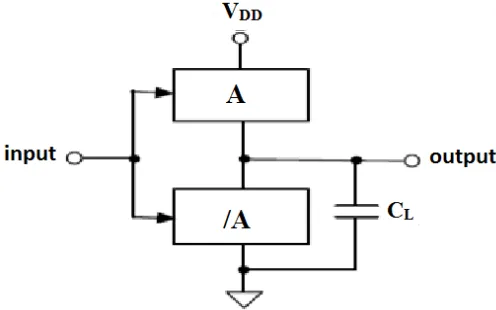
In CMOS logic design half of the power is dissipation in PMOS network and stored energy is dissipated during discharging process of output load capacitor during the switching events. Most of the power consumption reduction techniques are based upon scaling of the supply voltage, reducing capacitance and switching activity. Yet in all these cases, energy drawn from the power supply is used only once before being dissipated. Thus to increase the energy efficiency of logic circuits, a technique is required that can reuse the energy stored on load capacitor [3-4]. It has been found that there is a fundamental relation between computation and power dissipation. That is if somehow computation could be implemented without any loss of information, then the energy required by it could be potentially reduced to zero. This can be done by performing all computation in reversible manner. Also energy dissipation depends upon average voltage drop traversed by charge that flows on to the load capacitance. By using smaller voltage steps or increments dissipation can be reduced [5]. The minimum power consumption during the
[image:1.595.318.566.338.493.2]charge transfer phase is termed as adiabatic switching. In adiabatic logic charging is done by constant current source instead of constant voltage source as in conventional CMOS logic. It makes use of trapezoidal or sinusoidal waveforms as a power supply.
Fig 1: conventional CMOS logic circuit with pull up and pull down networks.
2.
Adiabatic Switching Principle
Conventional CMOS is very useful technology for low power digital circuit design due to its negligible static power. Dynamic power dissipation of CMOS circuits due to charging and discharging is proportional to load capacitance, square of the supply voltage and switching frequency. Capacitance and frequency factors increase the power consumption. Thus conventional CMOS design needs to be changed in order to satisfy the demand of low power supply. In Fig. 2 output load capacitance is charged by a constant current source instead of a constant voltage source used in conventional CMOS structures. This circuit is same as the equivalent model used in charging process in conventional CMOS. On resistance of pull up PMOS network is represented by R and C0 is the output capacitance [6]. It is noted that constant charging current corresponds to a linear voltage ramp. Energy dissipated through adiabatic logic is given as
C
V
T
T
RC
E
d C2
.
.
(2.1)
1) If charging period T is larger than 2RC then dissipated energy can be made smaller than Conventional CMOS circuit. Thus dissipated energy can be made arbitrarily small by
increasing the charging period, as
T
E
d1
.2) It has been noted that dissipated energy is proportional to resistance R instead of supply voltage and capacitance in conventional CMOS case. So energy dissipation can be minimized by reducing the on resistance through PMOS network.
.
Fig. 2 Equivalent model during charging phase in adiabatic circuits [6].
Hence by using constant current source energy can be transferred from supply to load capacitor with any dissipation and the energy stored on the load capacitance after charging process send back to the supply voltage by simply reversing the direction of current source [7]. Thus recycling is very attractive feature in adiabatic logic. The constant current supply must be capable of retrieving the charge back to the power supply. Adiabatic circuits does not use standard power supply instead of this it uses pulsating power supply which is also called as pulsed power supply [8].
3.
Compressor
A fast array multiplier is divided into three parts: a partial product summation tree booth encoder and a final adder. The partial product summation tree is responsible for total multiplication delay. Several techniques have been made to speed up the partial product summation tree by using various column compressors. These compressors simplify the interconnection circuitry. In multipliers 4-2 compressors, which have five input and three outputs are used. The carry out is connected to next 4-2 compressor’s carry in [7-8]. The 4-2 compressor can add four partial products because carry out does not depend on carry in. The 4-2 compressor is based upon a set of modified equations given as
4 3 2
1 X X X
X
S (3.1)
4 4 3 2 1 4 3 2
1 ) ( )
(X X X X C X X X X X
C in
(3.2)
1 2 1 3 2
1 ) ( )
(X X X X X X
Cout
(3.3)
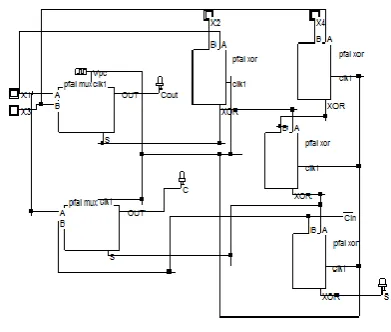
[image:2.595.316.493.78.233.2]An equivalent gate realization of 4-2 compressor using XOR and multiplexer is shown in fig. 3 contains five inputs and three outputs Cout, C and S [9-10].
Fig. 3 Compressor using XOR and Multiplexer [7].
4.
PROPOSED SCHEMATIC DESIGN
[image:2.595.63.259.202.290.2]The proposed design of compressor is based upon adiabatic logic, in proposed design PFAL logic is used which is made from two PMOS and two NMOS that avoids the degradation of the logic level at the outputs. These NMOS devices are connected between output node and ground. A sinusoidal supply is applied. This logic family also generates both positive and negative outputs. The functional blocks are in parallel with the PMOS of the adiabatic amplifier and form a transmission gate. The two n-trees realize the logic functions. This logic family also generates both positive and negative outputs [11]. The proposed compressor contains two modules: (i) a 2:1 adiabatic multiplexer (ii) an XOR gate based on adiabatic logic. A 2:1 multiplexer is designed using PFAL logic, it contains two inputs A, B one select line S and outputs out and out bar shown in fig. 4. A sinusoidal power clock is applied Vpc. When input is low, the output terminal ‘out’ follow the sinusoidal power clock [12-13].
Fig. 4 A 2:1 multiplexer using PFAL logic.
[image:2.595.317.529.476.590.2]Fig. 5 Timing simulation of 2:1 multiplexer.
[image:3.595.54.279.72.182.2]A two input XOR gate is designed using PFAL logic, it contains two inputs A and B and The minimum sized XORgate is implemented at 0.12µm technology. Circuit shown in the fig. 6 has complementary outputs. One is X-OR and other is X-NOR. 2 PMOS and 10 NMOS are used in this design, width of the PMOS is kept 2 times larger than the NMOS in order to get equal rise and fall times as mobility of electron is 2-3 times larger than holes [14-15].
Fig. 6 Design of a XOR gate using positive feedback adiabatic logic.
[image:3.595.322.518.79.245.2]Fig. 7 verfiy the logic behaviour of the X-OR circuit at 0.12µm technolgy [16]. Default gate and wire dealy is 0.030ns and 0.070ns respectivily. Elementary gate current is 500mA with supply voltage of 1.2V.
Fig. 7 Timing simultion of PFAL XOR/XNOR circuit.
The proposed 4-2 compressor is designed using two 2:1 multiplexer and four XOR gate. Multiplexer and XOR gate is implemented using positive feedback adiabatic logic. 4-2 compressor exhibits five inputs and three outputs [17-18]. DSCH 3.1 is used for schematic design shown in fig. 8.
Fig. 8 An adiabatic 4-2 compressor.
Timing simulation of 4-2 adiabatic multiplexer is shown in fig. 9, that logically verifies all the states of the compressor.
Fig. 9 Timing simulation of 4-2 adiabatic compressor.
5.
Layout Simulation
[image:3.595.57.298.321.458.2]Physical layout of a positive feedback adiabatic multiplexer is designed using Microwind 3.1 and simulation is performed using BSIM4 model. Layout of the circuit is achieved after compiling the verilog file, in the Microwind. A verilog file is a kind of netlist consisting all the components and connections used in designing of a circuit. Layout of multiplexer is shown in fig.10.
Fig. 10 Layout Representation of 2:1 adiabatic multiplexer.
[image:3.595.319.550.324.449.2]Fig. 11 Layout simulation of 2:1 adiabatic multiplexer.
[image:4.595.320.543.78.207.2]Layout structure of 2 input X-OR/X-NOR is obtained after compiling the verilog. Different metal layers are used, which includes metal1, metal2 up to six. For gate polysilicon layer is used. VDD and ground are made using metal1. Layout is shown in fig. 12.
Fig. 12 Layout representation of 2 input XOR/X-NOR circuit.
[image:4.595.55.289.87.213.2]Layout simulation of X-OR/X-NOR circuit is shown in fig. 13 The waveforms verify the correct logic of the circuit. Range of the voltage used for analog signal is 0-1.2V.
Fig. 13 Layout simulation of 2 input X-OR/X-NOR gate.
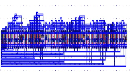
Layout out design of adiabatic multiplexer based 4-2 compressor is shown in Fig. 14. Layout is consists of two multiplexer and four EX-OR gates.
Fig. 14 Physical layout of adiabatic multiplexer based 4-2 compressor.
Layout simulation of adiabatic 4-2 compressor is carried out at 1.2 V. It is shown in Fig. 15. All results are simulated at 200 nano scale with a constant temperature of 270C. By using positive feedback adiabatic logic, full swing is obtained in output waveform. The frequency of applied sinusoidal clock is 250 MHz with 0.6 offset voltage.
Fig. 15 Layout simulation of multiplexer based adiabatic 4-2 compressor.
6.
RESULT & COMPARISON
[image:4.595.59.285.285.382.2]Dynamic power dissipated by CMOS and positive feedback adiabatic logic multiplexer is shown in table. In this table a CMOS multiplexer and an adiabatic multiplexer is compared at temperature of 270C. The inverter based on positive feedback adiabatic logic is power efficient than CMOS multiplexer discussed in table. 1.
Table 1. Comparison table of 2:1 Multiplexers.
Parameter Power Dissispation
Supply Voltage CMOS (µW) Adiabatic (µW)
1V 1.096 0.545
1.2V 1.848 0.932
1.4V 3.069 1.610
1.6V 4.932 2.727
1.8V 7.712 4.549
2V 11.761 7.255
[image:4.595.317.547.326.456.2] [image:4.595.55.292.469.602.2]power consumtion at supply voltage for the multiplexer. After foundary voltage thai is 1.2V, graph increases rapidly due to avlanche breakdown.
Fig. 16 Comparison of 2:1 multiplexers at different supply
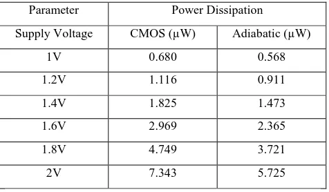
voltages.Dynamic power dissipation of CMOS X-OR and PFAL X-OR is compared in table. This comparison is performed at different supply voltage with a room temperature of 270. As the supply voltage increases power consumption increases in the same proportion. PFAL X-OR shows good performance at high voltage shown in table 2.
Table 2. Comparison table of adiabatic and CMOS based X-OR circuit.
Parameter Power Dissipation
Supply Voltage CMOS (µW) Adiabatic (µW)
1V 0.680 0.568
1.2V 1.116 0.911
1.4V 1.825 1.473
1.6V 2.969 2.365
1.8V 4.749 3.721
2V 7.343 5.725
The adiabatic 4-2 compressor is simulated and compared with conventional CMOS based compressor. Table 3 shows that adiabatic multiplexer based compressor is more power efficient than conventional one. Reults are verfied at different supply voltage.
Table 3. Comparison table of adiabatic and CMOS based compressor.
Parameter Power Dissipation
Supply Voltage CMOS (µW) Adiabatic (µW)
0.6V 4.426 0.596
0.8V 8.501 1.424
1V 13.989 3.481
1.2V 22.222 17.543
1.4V 38.389 30.956
[image:5.595.55.281.123.268.2]Fig. 17 shows the result of parametric analysis for CMOS and PFAL based compressors. It has been observed from the graph that PFAL compressor shows better result in terms of power consumption than conventional CMOS compressors.
Fig. 17 Power consumption vs supply voltage for CMOS and adiabatic compressors.
7.
CONCLUSION
4-2 compressor is designed using proposed adiabatic multiplexer which is designed with the help of four X-OR gate and two multiplexers. The proposed compressor is implemented using positive feedback adiabatic logic that saves power by recylcling the energy stored on load capacitor. This multiplexer based compressor is simulated at .12µm technology. The proposed adiabatic compressor saves 54.9% power at 1.2V than conventional CMOS based compressor design. It has been observed that proposed multiplexer saves 38.9% energy as compare to CMOS multiplexer. All results are verified at different supply voltage and temperature. Proposed Multiplexer based compressor shows good performance with supply voltage vs power consumption variations as compare to CMOS compressor.
8.
REFERENCES
[1] H. J. M. Veendrick, “Short-circuit Dissipation of Static CMOS Circuitry and its Impact on the Design of Buffer Circuits,” IEEE Journal of Solid State Circuits, pp. 468-473, August 1984.
[2] A. P. Chandrakasan, S. Sheng, R. W. Brodersen, “Low Power CMOS Digital Design,” IEEE Journal of Solid-state Circuits, Vol. 27, No. 04, pp. 473-484, April 1999.
[3] Micah C.Knapp, Peter J. Kindlmann, Marios C. Papaefthymiou, “Implementing and Evaluating Adiabatic Arithmetic Units,” IEEE Conference on Custom Integrated Circuits, pp. 115-118, 1996.
[4] M. Chanda, P. Sil, R. Mitra, A. Dandapat and H. Rahaman, “Comparative Analysis of Adiabatic Compressor Circuits for Ultra-Low power DSP application,” International Conference on Advances in Recent technologies in Communication and Computing, pp. 355-359, 2010.
[image:5.595.316.549.157.300.2] [image:5.595.49.287.399.538.2][6] Sung-Mo Kang, Yusuf Leblebici, CMOS Digital Integrated Circuits: Analysis and Design TATA McGRAW-HILL, pp. 197-519.
[7] Chip-Hong Chang; Jiangmin Gu; Mingyan Zhang ,“Ultra low-voltage low-power CMOS 4-2 and 5-2 compressors for fast arithmetic circuits,” IEEE Transactions on Circuits and Systems Vol. 51, pp. 1985-1997, October 2004.
[8] Yingtao Jiang, Al-Sheraidah, Yuke Wang, Edwin Sha and Jin-Gyun Chung,“A Novel Multiplexer-Based Low-Power Full Adder,” IEEE Transactions on Circuit and Systems-2nd:Express Brief, Vol. 51, pp. 345-348, July 2004.
[9] Suhwan Kim, Ziesler, Conrad H. Ziesler and Marios C. Papaefthymiou, “Charge-Recovery Computing on Silicon,” IEEE Transactions on Computers, Vol. 54, pp. 651-659, June 2005.
[10]Muhammad Arsalan and Maitham Shams, “Charge-Recovery Power Clock Generators for Adiabatic Logic Circuits,” IEEE Conference on Embedded System designs, pp. 171-174, 2005.
[11]Sambhu N.Pradhan, Gopal Paul, Ajit Pal, Bhargab B. Bhattacharya, “Power Aware BDD-Based Logic Synthesis Using Adiabatic Multiplexer,” IEEE Conference on Electrical and Computer Engineering, pp. 149-152, December 2006.
[12]Yasuhiro Takahashi, Youhei Fukuta, Toshilkazu Sekine, Michio Yokoyama, “2PADCL: Two Phase drive
Adiabatic Dynamic CMOS Logic,” IEEE Conference on Circuits And Systems, pp. 1484-1487, 2006
.
[13] Hsiao-EnChang, Juinn-Dar Huang, Chia-I Chen, “Input Selection encoding for Low Power Multiplexer Tree,” IEEE Conference on VLSI Design Automation and Test, pp. 1-4, 2007.
[14] Cihun-Siyong Alex Gong, Muh-Tian Shiue, Ci-Tong Hong and Kai-Wen Yao, “Analysis and Design of an Efficient Irreversible Energy Recovery Logic in 0.18-µm CMOS,” IEEE Transactions on Circuits and Systems,” Vol. 55, NO. 9, pp. 2595-2607, October 2008.
[15] Etienne Sicard, Sonia Delmas Bendhia, Basic of CMOS Cell Design, TATA Mc GRAW-HILL, pp. 51-90.
[16] Etienne Sicard, Sonia Delmas Bendhia, Advance of CMOS Cell Design, TATA Mc GRAW-HILL, pp. 80-87.
[17] Etienne Sicard, Sonia Ben Dhia, Syed Mahfuzul Aziz, “Teaching CMOS Circuit Design in Nanoscale Technologies Using Microwind,” Proceedings of the European workshop on microelectronics education, pp. 78-83, May 2010.
![Fig. 2 Equivalent model during charging phase in adiabatic circuits [6].](https://thumb-us.123doks.com/thumbv2/123dok_us/8062256.776769/2.595.316.493.78.233/fig-equivalent-model-charging-phase-adiabatic-circuits.webp)