Design of High Speed Full Adder using Improved
Differential Split Logic Technique for 130nm Technology
and its Implementation in making ALU
Gurleen Kaur
Mtech Microelectronics UIET, Panjab University
Chandigarh, UT India
Arvind Kumar
Assistant Professor, ECE UIET, Panjab University
Chandigarh, UT India
Jatinder Singh
Assistant Professor, ECE UIET,Panjab University
Chandigarh,UT India
ABSTRACT
Adders are the main components in digital designs which are used not only for addition but can be used for multiplication and division too. Adders find use in very large scale integrated circuits from processors (like in arithmetic logic circuits) to application specific integrated circuits. At the same time, high speed computation has become the important part of any digital applications today though low power is a key factor too. In this paper, a high speed full adder using improved differential split logic (DSL) technique is used. We further implement it in 1bit arithmetic logic circuit (ALU). Measurements show that proposed full adder is better than DSL full adder in terms of speed, and further implementation of it in ALU shows that it is better than CMOS ALU in terms of speed, power and power delay product (PDP).
General Terms
Full adder, Differential split level logic (DSL), Differential cascade voltage logic (DCVS), Arithmetic logic circuit (ALU), Power delay product (PDP), Full adder (FA), Multiplexer (Mux).
Keywords
Differential Split logic, Full adder, Arithmetic logic circuits
1.
INTRODUCTION
Full adders are the heart of all arithmetic calculations [13]. It is a combinational logic unit that performs all the calculations like addition, subtraction, increment and decrement. There are certain factors that can simply slow down the development of small complex IC chips. These factors are design cost, design productivity and IC fabrication technology. The increasing demand for high speed very large scale integration can be obtained at design levels such as architectural, circuit and layout level .For the circuit design, at this level a proper choice of logic design style for high speed combinational logic circuits should be done. It is because all the important parameters affecting speed are switching capacitance, transition activity and short circuit currents are actually influenced by the chosen logic style. Earlier the parameters like power dissipation, small area and cost factor were given more weight age , but now days speed considerations are also the important factors for the scientific community related to VLSI designs.
In CMOS technology, even if we design high speed full adder, power dissipation is also taken care of. Power dissipation is one of the critical factors which is of two types and is classified into dynamic power and static power. Dynamic power dissipation comes into picture when the circuit is
operational and static power dissipation is considered when the circuit is inactive.
Dynamic power is further classified into switching power (Pswitch) and short circuit power (Psc).Static power is because of
leakage power dissipation [7].
There are three major sources of power dissipation which are given in the following equation.
Ptotal .Cl.Vdd .fclk Isc.Vdd Ileakage.Vdd
2
The first term shows the switching component of power where α is the switching factor, Cl is the loading capacitance,
fclk is the clock frequency. The second term represents the
dissipation due to short circuit currents. The last term is the dissipation due to leakage currents ( Ileakage )[1].
The switching power dissipation in CMOS digital integrated circuits is an important function of the power supply voltage Vdd Reduction of power supply voltage is an important way to
limit the power dissipation. But then limiting the power dissipation, results in increased circuit delay. The given equation tells about the dependence of delay on power supply voltage:
T
d
C
lV
ddk
(
V
dd
V
th)
Where k = transistor aspect ratio (W/L),Vth= transistor
threshold voltage, α = velocity saturation index which varies between 1 and 2.
On decreasing the power supply voltage, power dissipation though is reduced, but instead the delay increases as the threshold voltage reaches near the supply voltage. This problem is overcome by using the low power differential split logic technique.
Section II gives a brief introduction of conventional full adder and the various logic styles that can be used to make full adders. Section III describes about the propagation delay analysis in DCVS and DSL circuits.
Section IV describes about the proposed DSL full adder and its implementation using the Tanner v 13.0 tool.
Section V further discusses about the implementation of these adders in designing arithmetic logic circuit.
2.
LOGIC DESIGN STYLES
2.1
Conventional CMOS
The schematic diagram of a conventional CMOS adder is shown in the given figure:
Fig 1: CMOS full adder [2]
Signals noted with ‘-‘are basically complementary signals. The width of the transistors is increased to obtain a reasonable conducting current to drive the capacitive loads which further results in increased capacitance and high propagation delay.
2.2
Complementary pass transistor logic
The schematic diagram of CPL adder is shown in the diagram. .
Fig 2: CPL full adder [2]
In CPL, the logic functions are implemented by the use of only an NMOS. This basically results in low input capacitance and high speed operation.CPL circuits consume less power than conventional static logic circuits because the logic output voltage swing of the pass transistor is less than the supply voltage level.
2.3
Differential cascode voltage switch
logic (DCVSL)
DCVS have reduced transistor counts over NAND/NOR implementations. DCVS has got better performance of about 4times as compared to the CMOS/NMOS NAND/NOR circuits and maintaining the low power circuitry. The schematic diagram of the full adder is shown
Two complementary NMOS transistors set of switching trees are designed to connect to a couple of cross coupled PMOS transistors. One of the outputs is pulled down by NMOS network depending on the differential inputs. The input capacitance is two or three times smaller than that of conventional CMOS adder because the inputs drive only the NMOS transistors.
2.4
Differential split level logic (DSL)
Two NMOS transistors with their gates connected to the reference voltage are added to reduce the logic swing at the output nodes.
V
ref
(
V
dd/
2
)
V
thWhere Vth = NMOS threshold voltage.
So the output nodes are clamped at the half power supply voltage, hence the operation of the circuit becomes faster than the DCVSL operation. But these circuits dissipate high static power dissipation due to the incomplete turn off of the cross coupled circuits. Addition of two more NMOS transistors results in the increase of area. The circuit diagram of DSL full adder is shown.
Fig 4: DSL full adder [2]
3.
DELAY IN DSL
Fig 5: Basic DSL circuit
Fig 6: Input /output waveforms of half DSL circuit
The given figure of half DSL logic circuit is considered for the delay analysis.
Fig 7: Half DSL circuit
Voltage change at Q is (0.5Vdd-Vx). Hence, if C1 is the capacitance at Q and IC1, the current which charges it during the propagation delay then td can be expressed as:
T
d
C
l(
0
.
5
V
dd
V
x)
/
I
c1Moreover td can be expressed in term of the current of Ipmos which flows through P2 during the propagation delay, which not only charges the capacitance at C1 but also charges the capacitance at node Fn. Referring to the capacitance C2, voltage change across it during the propagation delay td is Vfn. Considering the Ipmos ,td is expressed as follows :
T
d
(
C
l(
0
.
5
V
dd
V
x)
C
2(
V
fn))
/
I
pmos WhereV
fn
K
(
V
ref
V
tn2)
K
A
B
(
C
2/
C
1)
2
)
)
(
)(
2
/
(
)
/
(
n n dd ref tn tppmos
W
L
A
V
B
V
V
V
I
4.
IMPLEMENTATION OF PROPOSED
FULL ADDER
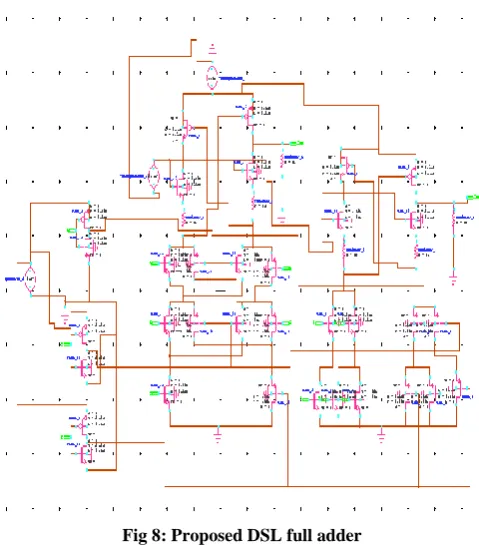
In this modified DSL full adder is proposed. Two resistors are added in series to the reference NMOS N10 and N20 transistors in the DSL circuit in figure 5which will switch on the PMOS transistors more quickly .This helps in decreasing the delay in the full adder. The worst case delay is considered for the measurements. The transistor W/L ratio is 1.66.Tanner v13.0 too is used with the 130nm technology file. The schematic diagram of the proposed full adder is shown.
Fig 8: Proposed DSL full adder
The above proposed full adder is further modified by putting capacitor in parallel with the resistors that are added in series to the reference transistors in figure 9.
Fig 9: Proposed DSL full adder with capacitance
4.1
Simulation Results
Table 1.Delay (10-10ns) calculations wrt increasing resistance (ohms)
Resistan ce
Delay(C=0 pF)
Delay(C=0.000 1pF)
Delay(C=0.00 1pF)
0 1.4846 1.4846 1.4846
100 1.4577 1.4577 1.4577
200 1.4341 1.4341 1.4343
300 1.4220 1.4220 1.4224
400 1.4104 1.4104 1.4109
500 1.3977 1.3978 1.3986
1000 1.3449 1.3452 1.3481
1100 1.3306 1.3309 1.3343
1200 1.3224 1.3231 1.3285
1300 1.3170 1.3177 1.3181
1400 1.3149 1.3108 1.3179
1500 1.3156 1.3164 1.3202
1600 1.3182 1.3191 1.3241
1700 1.3099 1.3111 1.3218
1800 1.3034 1.3046 1.3160
[image:4.595.74.550.93.721.2]1900 1.2993 1.3007 1.3127
Table 2.Power consumption (µw) calculations wrt increasing resistance (ohms)
Resista nce
Power(C=0 pF)
Power(C=0.000 1pF)
Power(C=0.00 1pF)
0 7.977327 7.977327 7.977327
100 8.59742 8.597420 8.597418
200 9.220806 9.220805 9.220798
300 9.845852 9.84585 9.845835
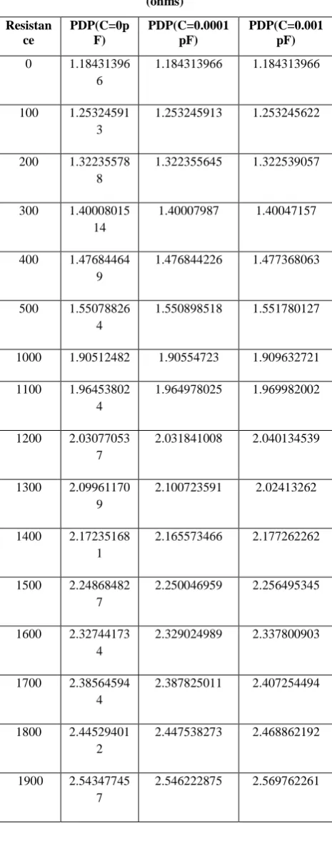
Table 3.PDP (µw ns) calculations wrt increasing resistance (ohms)
Resistan ce
PDP(C=0p F)
PDP(C=0.0001 pF)
PDP(C=0.001 pF)
0 1.18431396 6
1.184313966 1.184313966
100 1.25324591 3
1.253245913 1.253245622
200 1.32235578 8
1.322355645 1.322539057
300 1.40008015 14
1.40007987 1.40047157
400 1.47684464 9
1.476844226 1.477368063
500 1.55078826 4
1.550898518 1.551780127
1000 1.90512482 1.90554723 1.909632721 1100 1.96453802
4
1.964978025 1.969982002
1200 2.03077053 7
2.031841008 2.040134539
1300 2.09961170 9
2.100723591 2.02413262
1400 2.17235168 1
2.165573466 2.177262262
1500 2.24868482 7
2.250046959 2.256495345
1600 2.32744173 4
2.329024989 2.337800903
1700 2.38564594 4
2.387825011 2.407254494
1800 2.44529401 2
2.447538273 2.468862192
1900 2.54347745 7
[image:5.595.308.559.333.736.2]2.546222875 2.569762261
Fig 12: Graph for PDP with increasing resistance
4.2
Comparison results of proposed FA
The performance parameters of proposed full adder are compared to the ones given in the paper [10].
Table4. Comparison of performance parameters of FA
Logic circuits Delay(ns) Power(µw) PDP(µw ns)
Proposed FA 0.12 19.57 2.569762261
DSL FA 0.148 7.977327 1.184313966
CMOS FA 0.12 73.8 8.856
CPL FA 0.11 39.1 4.301
DCVSL FA 0.13 110.7 14.391
P-CPL FA 0.18 21.3 3.834
P-DCVSL FA 0.2 103 20.06
5.
DESIGN OF ALU USING PROPOSED
FULL ADDER
Arithmetic logic unit is designed using the proposed full adder for arithmetic unit. This adder is used for addition, subtraction, increment and decrement by controlling the data inputs to implement these operations [9].Moreover for logic unit AND, OR, XOR and inverter is designed using modified DSL logic which is used in full adders too [11]. For designing ALU, two 4:1 mux and one 2:1 mux are designed using DSL logic [12]. So eight operations are performed by using this ALU shown in table 5.
Fig 14: Structure of ALU
Table5. Truth table for ALU
Fig 15: 4:1 Mux circuit schematic
Fig 17: OR circuit schematic
Fig 18: XOR circuit schematic
Fig 19: ALU circuit schematic
The output is taken across 2:1 mux [8]. The propagation delay, power dissipation and power delay product are calculated with power supply voltage as 5.0v and reference voltage as 2.58V provided to reference NMOS transistors.
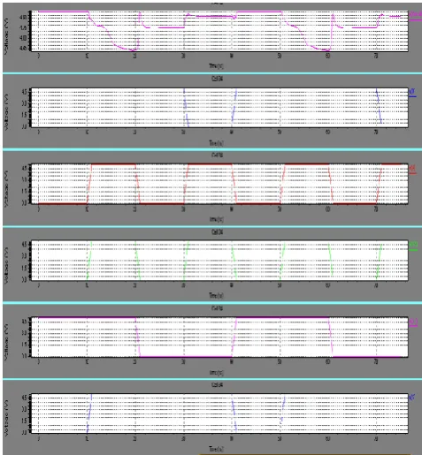
Fig 20: Simulation waveforms of ALU in W-edit
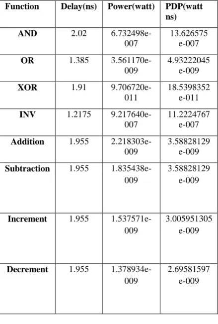
[image:7.595.314.553.424.682.2]Table 6. Performance parameters of ALU
Function Delay(ns) Power(watt) PDP(watt
ns)
AND 2.02
6.732498e-007
13.626575 e-007
OR 1.385
3.561170e-009
4.93222045 e-009
XOR 1.91
9.706720e-011
18.5398352 e-011
INV 1.2175
9.217640e-007
11.2224767 e-007
Addition 1.955
2.218303e-009
3.58828129 e-009
Subtraction 1.955
1.835438e-009
3.58828129 e-009
Increment 1.955
1.537571e-009
3.005951305 e-009
Decrement 1.955
1.378934e-009
2.69581597 e-009
6.
CONCLUSION
The proposed full adder has better performance in terms of delay. It is observed with the simulation results that with adding resistor, propagation delay decreases in a fast way. But it is observed that on addition of capacitor in parallel to the resistor added in the circuit, the delay decreases gradually and the power dissipates more but less gradually in comparison to the modified full adder with added resistance only. Since priority is high speed, proposed full adder with only added resistor is used in designing ALU .After the analysis , the other components of ALU are designed with same modified DSL logic technique This proposed ALU can be used for high speed and low power applications.
7.
REFERENCES
[1]A. P. Chandrakasan, S. Sheng and R. W. Brodersen, “Low Power CMOS Digital Design,” IEEE Journal of Solid-state Circuits, vol. 27, No. 4, pp. 473-484, April 1999.
[2]Dimtrios Soudris,Christian Piguet,Costas Goustis, “Designing CMOS Circuits for Low Power (European Low-Power Initiative for Electronic System Design (Series))” ,Kluwer Academic Publishers,Oct 2002,pp.74-7t8
[3]P.Sheridan,C.M.Huizer,“AnExpression for the propagation delay of a Differential Split-Level (DSL) CMOS Logic Gate”,IEEE Journal of solid state circuits,Vol-22,No.3, June1987,pp.457-459
[4]Leo C.M.G. Pfennings,Etal.,“Differential Split Level CMOS Logic for Subnanosecond Speeds,” IEEE Journal of Solid State Circuits, Vol. SC-20, No.5, Oct 1985,pp.1050-1055.
[5]Didem Z. Turker, Sunil P.Thakur, Edgar Sánchez-Sinencio ,“A DCVSL Delay Cell for Fast Low Power Frequency Synthesis Applications”, IEEE Transactions on circuits and systems-I:Regular papers, June 2011, Vol. 58, No. 6,pp. 1225-1238
[6]S. M. Aziz, W. A. J. Waller, “On testability of Differential Split-Level CMOS Circuits”, IEEE Proc.-Circuits Devices Syst., Vol. 141, No. 6, Dec 1994,pp.191-194 [7]L.G Heller, Etal.,“Cascode Voltage Switch Logic: A
Differential CMOS Logic Family”, Proceedings of 1984 IEEE International Solid-State Circuits Conference, pp. 16-17.
[8]Ila Gupta,Neha Arora,Dr.B.P.Singh,“Design and analysis of 2:1 multiplexer for high performance digital systems’’, IJECT, Vol. 3, Issue 1, Jan-March 2012 [9]Daniel D.Gajski, “Principles of Digital Design’’,Prentice
Hall publishers,1997,pp.178-182
[10]Weiqiang Zhang, LinfengLi,Jianping Hu,“Design Techniques of P-Type CMOS Circuits for Gate-Leakage Reduction in Deep Sub-micron ICs”,IEEE International Midwest Symposium ,Circuits and Systems, 2009. MWSCAS '09,2-5Aug, 2009, pp.551-554
[11]Dae Woon Kang,Yong-Bin Kim,“Design of enhanced differential cascode voltage switch logic(EDCVSL) circuits for high fan-in gate’’,ASIC/SOC conference,2002,15th annual IEEE international,25-28sept 2002,pp.309-3013.
[12]Nehru K.,Shanmugam,A., Darmilathenmozhi,G.,“Design of low power ALU using 8T FA and PTL based MUX circuits’’,Advances in Engineering,Science and Management(ICAESM),IEEE international conference,30-31 march 2012,pp.724-730.
[13]M. Morris Mano,“Digital Logic design” ,Prentice Hall publishers, Aug 2001,pp.116-120