Neural Network Simulation of Digital Circuits
D. P. Sharma
Professor, Dept. of Computer Science,
Dean, Sciences.
St. Joseph’s College, Hyderabad, India
ABSTRACT
This paper discusses the process of behavioral conversion of digital circuits used for signal processing applications into its neural network counterpart[1][2]. The neural network so
devised represents simulated digital circuits without any deviation in its input–output characteristics. However, the design of such networks depends entirely on different parameters and thus the design process too. It is believed that, if designed properly, the software format of neural network will be helpful in replacing various important hardware circuits in the digital systems calls for precision[4][5].
General Terms
Neural Networks representation of digital circuits, Digital Circuit Simulation.
Keywords
Digital Circuits, Neural Networks, Discrete Circuit conversion.
1. INTRODUCTION
Neural Networks are quiet effective in simulating the digital circuits. The Neural Network representation can be used in multiple applications where the digital circuit behaviors are required to be presented in computer software form as solution to certain specific problem[2][4].
2. DIGITAL CIRCUIT CONSIDERATION
Half AdderThere are several integrated circuits that perform arithmetic functions, e.g., addition, subtraction, multiplication, and division. Here we will examine the digital circuit of Half Adder and its Neural Network counterpart[5][6][7].
The Half Adder circuit is a basic arithmetic circuit. To understand its operation, let us first examine addition of two one bit words that results in two bits of data, that is, the sum bit and a carry bit. We are considering the generalized case where addition of two bits of information always results in a sum and a carry. For instance, 0 plus 0 results in a sum of 0 and a carry of 0.
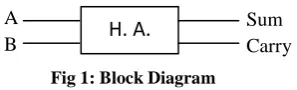
[image:1.595.329.509.253.336.2]Considering the block diagram of Half Adder, we find it more straight and clear that the inputs A and B yields two outputs, that is, the Sum and Carry. The sum and carry are conditional which is reflected in the truth table, see figure 3.
Fig 1: Block Diagram
Further this block diagram can be converted to the circuit diagram to understand it vividly and more technically. We use here the XOR gate for “Sum” output whereas we use a simple
[image:1.595.370.477.466.588.2]AND gate for “Carry” output. The arrangement of the digital circuit is as shown in the figure 2 below.
Fig 2: Logic Diagram of Half Adder
The truth table can be constructed to show each row as one condition of A and B resulting in sum and carry. The sum is exclusive OR of A and B. Thus, to add is to XOR.
The Sum is represented in Boolean logic as The carry is represented as: A.B Thus, the truth table reflecting both sum and carry is given below:
A B Sum Carry
0 0 0 0
0 1 1 0
1 0 1 0
[image:1.595.334.538.626.731.2]1 1 0 1
Fig 3: Truth Table of Half Adder
The Neural Network counterpart of the above digital circuit can be given as:
Fig 4: Neural Network counterpart of Half Adder
A B
Sum Carry
H. A.
W6=1 W1=1
W2=1 W3= -1
W4= -1
W5=1
W7=1 W8=1
a
b
Z0
Z1
Z2
Z3
Sum
Carry
y
outA
B Sum
[image:1.595.100.249.683.728.2]The Neural Network used is Feed Forward Neural Network (FFNN) for easy and straight representation of the digital circuits.
Now, let us design the activation function of the proposed Neural Network bearing in mind the following input equations for each node. For instance, at neuron Zi the input is defined
as:
b.wi
-a.wi
=
yin(Zi)
or,
and the node output is given by the activation function:
There is a self imposed restriction in the network that the output, that is, f(Z3)will not go beyond 1. But for neuron Z2
the activation function will have to be assigned the following terms:
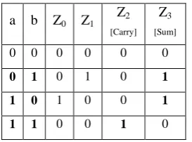
Evaluating yin for Z0, Z1, Z2, and Z3, we get the following
truth table for the network giving values for yout. For each
input pair a and b:
a b Z0 Z1 Z2 Z3
[image:2.595.107.226.415.505.2]0 0 0 0 0 0 0 1 – 1 1 0 1 1 0 1 – 1 0 1 1 1 0 0 2 0
Fig 5: Truth Table for the network shown in Figure 4.
This table can be revised according to the definition of activation function (
y
out) given above.a b Z0 Z1
Z2 [Carry]
Z3 [Sum]
0 0 0 0 0 0
0 1 0 1 0 1
1 0 1 0 0 1
[image:2.595.100.237.569.670.2]1 1 0 0 1 0
Fig 6: Revised Truth Table given in Figure 5.
Please note that, in the last row of the table, the threshold is defined as ≥ 2. Thus, neuron at Z0 node will fire up.
We, therefore, find the proposed neural network is completely equivalent to the Half Adder circuit comparing the outputs of both the concepts.
2.1 Formulating Node Responses
First Order Predicate Logic (FOPL) is found to be adequate enough to formulate the nodes’ responses since it considers the premise of a given argument and its outcome directly as cause and effect relation. This makes it easy to represent “excitation” and “inhibition” of neurons in a neural network under various conditions of inputs. Thus, formulating responses of the neuron nodes Z0, Z1, Z2, and Z3, in relation to
“sum” and “carry” as in case of half adder, we get –
Sum f(Z3) for input vectors α and β respectively (0,0), (0,1), (1,0) and (1,1) respectively:
For vectors (0),(0)a,b:(((a)(b))(f(Z3))) For vectors (0),(1)a,b:(((a)(b))(f(Z3))) For vectors (1),(0)a,b:(((a)(b))(f(Z3))) For vectors (1),(1)a,b:(((a)(b))(f(Z3))) Carry f(Z2) for input vectors α and β respectively (0,0), (0,1), (1,0) and (1,1) respectively:
For vectors (0),(0)a,b:(((a)(b))(f(Z2))) For vectors (0),(1)a,b:(((a)(b))(f(Z2))) For vectors (1),(0)a,b:(((a)(b))(f(Z2))) For vectors (1),(1)a,b:(((a)(b))(f(Z2))) The above relations are in compliance with the truth table shown in figure – 5. Here
φ
denotes fallacy andstands for tautology. Thus, the premise of given arguments shows
φ
for inhibition and for excitation of neurons.We next consider another example of interest, that is, the circuit design of Convolution Encoder using Reverse Viterbi (RV) algorithm[3].
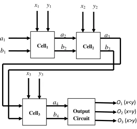
Figure 7 shows the logic circuit design of an iterative network to compare two 3–digit binary numbers: X = x1x2x3 and Y = y1y2y3, and figure 8 presents the detailed synthesis of a comparator circuit (fig. 8.a) which is made of a comparator cell and a comparator output circuit (fig. 8.b). The extension of the circuit in figure 7 to compare two n-digits binary numbers is quiet clear by utilizing n-cells and the same output circuit.
Figure 7 Iterative network to compare 3-digit binary numbers
Figure 8(a) and 8(b) are discrete circuit representations that carry the comparisons as given in the figure 7. It shows the arrangements of digital components in the circuit that perform the task of comparisons.
Fig 8(a): Comparator Cell
Fig 8(b): Comparator Output Circuit
The Neural Network can be presented using the concept we have utilized in our previous discussion. Thus, the proposed Neural Network can be given as:
Fig 9: Neural Network representation of iterative network comparator
Each neuron must be taken into consideration to be a perfect representative of specific section of the digital counterpart. Let us consider a case for digital circuit conversion to BPN. In my opinion, it will provide more insight to the design methodologies.
Case – 1: Detection and Correction of forward errors in digital transmissions: Block Parity.
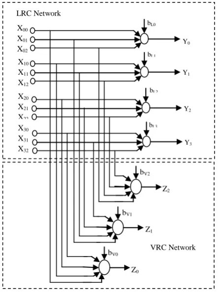
In this method the data block is arranged in a rectangular matrix and two sets of parity bits are generated, i.e., Longitudinal Redundancy Check (LRC) and Vertical Redundancy Check (VRC). VRC is the parity bit associated with the character code and LRC is generated over the rows of bits, LRC is appended at the end of the data block. Here we will use even parity for both LRC and VRC.
[image:3.595.56.283.79.292.2]Let us take example of a data block, to be transmitted, for the purpose of analyzing it and designing an appropriate neural network for the same.
Figure 10 Data Block
[image:3.595.46.291.381.682.2]On receiving the data block at the transmitting end, the LRC and VRC bits will be added to it before transmitting it.
Figure 11 Schematic diagram for Parity Bit Insertion
J
0J
1J
2i
01 0 0
i
11 0 1
i
21 1 1
i
30 0 1
O3 (x>y)
O2 (x=y)
O1 (x<y)
a
1b
1
a
2b
2
a
3b
3
a
4b
4
x1 y1 x2 y2
x3 y3
Cell1 Cell2
Cell3 Output
Circuit
Celli
bi+1
ai+1
y
ix
iai
bi
O1(x<y)
O2(x=y)
O3(x>y)
a
n+1b
n+1Data Block
Insertion of LR Parity Bit
Insertion of VR Parity Bit
O1(x<y)
O3(x>y)
M=O2(x=y)
M
w 9
w10
w11
X 1
a 1
b 1
y 1
w1
w2
w5
w6
w7
w8 w3
w4
A4 A2
A3 A0
A1
[image:3.595.390.466.523.604.2] [image:3.595.321.540.647.724.2]Figure 12 Insertion of Vertical and Longitudinal Parity Check Bits
Bits transmission sequence: 11101 00101 01111 10111
2.2 Block Check and Correction of
Redundancy
On receiving data block through transmission the VRC and carried to see if it is erroneous. If it is erroneous then the signal is reconstructed to extract the data originally transmitted.
Block check and data reconstruction schema can be presented in the schematic diagram given in figure 13.
However, the above discussed concepts can be translated into design of an efficient BPN to be used for both the parity bits insertion before data transmission and to carry the parity checks and data reconstruction on receiving the transmitted signals.
Figure 14 BPN Network for insertion of Parity Bits, Block Check and Data Reconstruction
It is to be noted that there is a little change in the application of the algorithm produced here under, for the purpose of insertion of parity bits (LRC and VRC) and while carrying check and correcting erroneous data bit on interception of signals after its transmission. Thus, it must be dealt with carefully.
The algorithm for the proposed network can be presented as: LRC segment algorithm –
1. Initialize all biases to zero.
2. Check the output of each neuron using:
yi =
n jLi ij
b
x
0
n= no. of cols. (j), i= row
3. Insert the LRC bits as per the condition given: 1, if yi mod 2 = 1
bL0 = 0, if yi mod 2 = 0
1, if yi mod 2 < 0
VRC segment algorithm – 1. Initialize all biases to zero.
2. Check the output of each neuron using:
Even Parity Bits (VRC)
Even Parity Bits (LRC)
1
0
0
1
1
0
1
0
1
1
1
1
0
0
1
1
[image:4.595.62.243.80.239.2]1
1
1
1
Figure 13 Schematic diagram for Block Check and Data Reconstruction
Intercepted Signals
Errorless Signal Output
Y
N
Reconstruct Erroneous Data Data Block with
Parity Bits
LRC Check VRC Check
ERROR
LRC Network
VRC Network bV2
bV1
bV0
Z2
Z1
Z0
bL0
bL1
bL2
bL3
Y0
Y1
Y2
Y3
X00
X01
X02
X10
X11
X12
X20
X21
X22
X30
X31
[image:4.595.60.282.396.551.2]zj =
n iVj ij
b
x
0
n= no. of rows. (i), j= cols.
3. Insert the VRC bits as per the condition given: 1, if zj mod 2 = 1
bV0 = 0, if zj mod 2 = 0
1, if zj mod 2 < 0
On interception of signals the data check and correction is carried as:
Assuming the data at xij is erroneous (say, instead of zero it
has become 1), then carry LRC check taking mod of the individual row to see whether it is even or odd. Mark the row data (xij) if its sum: ((
n
j
Li ij
b
x
0
) mod 2 ≠ 0).
Similarly, carry VRC check taking mod of the individual row to see whether it is even or odd. Mark the row data (xij) if its
sum:
((
n
i
Vi ij
b
x
0
) mod 2 ≠ 0).
The data at intersection of the marked row and column is The time response of the circuit is 0.0000541 seconds on 2.90 GHz Intel processor (3.41 GB RAM).
erroneous and has to be corrected using following algorithm: 0, if xij = 1
1, if xij = 0
Important:
1. Synaptic weight is kept “1” as identity element for the input signal.
2. Bias updating is carried through error back-propagation checking whether the even parity is maintained or not. 3. Target value of the individual neuron is ascertained through bias updating keeping in view the even parity requirement.
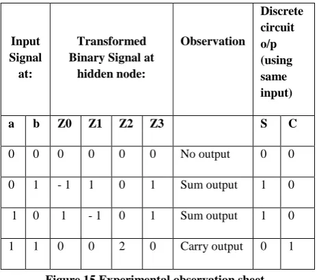
3. EXPERIMENTAL ANALYSIS
Experimental detail of simulation of Half Adder hardware and neural network circuits given in figure 2 and 4:
Input Signal
at:
Transformed Binary Signal at
hidden node:
Observation
Discrete circuit o/p (using same input)
a b Z0 Z1 Z2 Z3 S C
0 0 0 0 0 0 No output 0 0
0 1 - 1 1 0 1 Sum output 1 0
[image:5.595.315.547.70.274.2]1 0 1 - 1 0 1 Sum output 1 0 1 1 0 0 2 0 Carry output 0 1
Figure 15 Experimental observation sheet
Thus, the input-output characteristic of the given neural network circuit for Half Adder exhibit the adaptation of behavior of its hardware gate circuit counterpart. The hidden layers: Z1, Z2, and Z3 of the neural network indicate the actual processing of the inputs given to it, which can be had by calculating (inserting print line in program code) the signal at specific hidden node using mathematical relations shown for the respective node.
Time Response of NN versus Discrete Circuit The time response of corresponding hardware circuit as given in figure 2 is 0.0000551 seconds, thus providing a lag of 0.0000010 seconds.
Here, we have taken n number of pairs of discrete circuit and neural network to evaluate the time lag between them. In each case the time lag obtained is: TNN < Tdiscrete, and TNN -Tdiscrete =
[image:5.595.335.501.481.627.2]δx, where x ≥ 0.
Figure 16 Time Response Gantt Chart
Since δa ≈ δb ≈ δn, thus it can be generalized that the discrete circuits are not as fast as its neural counterparts since certain time lag (δx) is significant.
4. DESIGN CONSIDERATIONS
The designing of Neural Network as simulator of digital circuits require certain important considerations. In this paper only forward pass of FFNN is considered to meet the requirements of the digital circuits under consideration. However, the designer may choose from among various architectures of the network as per suitability of the requirement, such as – BPN[8], ART NN, etc[9][10]. More importantly, the selection of specific network also depends on
X
ij=
time NN
DC
NN DC
NN DC
nature and complexity level of specific circuit. Further consideration must be given to the suitability margin of a digital circuit for its neural network implementation.
The parameters that need special emphasis while considering designs of such systems are:
i. Threshold: it determines the firing limit of neuron which is important in achieving the output characteristics required in the network so designed.
ii. Activation Function: It must properly be designed since the behavioral aspects of the network depend completely on this function. One may choose out of many standard functions too, such as – Step function, Sigmoid / Logistic function, Hyperbolic Tangent function, Gaussian Radial Basis function, etc.
iii. Synaptic Weights: It is yet another important consideration that determines the type and magnitude of inputs required in a specific part of the network. Synaptic weight is a functional element of the network that works in conjunction with the threshold to make the network adopt the expected behavioral outcome.
Since there is a complete paradigm shift while considering design conversion from digital to NN counterpart, thus the designer must bear in mind the followings:
1. Only the functional aspects of a digital circuit are the suitable candidate for translation to its neural network counterpart.
2. I/O characteristics of the digital circuit is one of the most important factors to be considered for proper designing. 3. The design conversion may require proper refractor of digital circuit under consideration, as it is normally in case of larger and complex circuits.
4. Before finalizing the design, sufficient consideration must be given to the relative cost factor to ascertain feasibility of such design conversion from digital to neural network.
5. COST CONSIDERATION
So far the cost consideration is there, this is supposed to cut down cost of hardware it replaces to minimize it down to lowest possible estimated level, that is, as per a rough estimation it is somewhere around in the ratio of 1:15 to 1: 49, depending on the utility of digital components used in the actual hardware circuit.
6. FUTURE SCOPE OF THE WORK
At the lab scale, it is found to be quiet suggestive as best alternative of discrete hardware circuits in a number of cases, with significant cut in response time as well as in terms of cost. Its design time is much less than the hardware circuits. It also has the qualification to stand against ageing, wear and tear and maintenance problems. However, it requires more study to be carried in specific cases to establish its synergistic effect and appropriateness.
It can primarily be used to replace certain digital hardware circuits in an effective way[11][12][13]. Thus, in case of digital circuits working on principles of fuzzy system it will be more suitable to be used[14].
Since it is quiet promising with regard to both the speed and effective cost reduction, this conversion technique from discrete to neural counterpart can easily be utilized in multiple small as well as big circuits such as – modem, time controlled circuits, function controlled circuits, real time application circuits, etc.
7. ACKNOWLEDGEMENT
My sincere thanks to my colleagues researchers who are always of great help to me while discussing the critical issues, especially to my wife Prof. Shweta who always critically examine and discusses all of my research manuscripts in favour of improving it and making it flawless to the possible extent.
REFERENCES
[1] Claus Svarer, 1995. Neural Networks for Signal Processing, Ph. D. Thesis, CONNECT Electronics Institute, Technical University of Denmark.
[2] Miona Andrejević and Vančo Litovski. Electronic Circuits Modeling using Artificial Neural Networks.
Journal of AutomaticControl, University of Belgrade,
VOL. 13(1):31-37, 2003.
[3] Jongmin Kim, John J. Hopfield, and Erik Winfree. Neural Network Computation by in Vitro Transcriptional Circuits. California Institute of Technology. 2004. [4] Philips Research Laboratories. Eindhoven. Neural
Network Applications in Device and Sub-circuit Modeling for Circuit Simulation. Netherlands. 2003. [5] Jason M. Kinser. and Thomas Lindblad, 1997
Implementation of Pulse-coupled Neural Networks in a CNAPS Environment. Technical Paper. No - 10.1.1.45.4239. Royal institute of Technology, Sweden. [6] Jan Michalik, 2009. Applied Neural Network for Digital
Signal Processing with DSC TMS320F28335. VSB-Technical university of Ostrava.
[7] Yu Hen Hu and Jenq-Neng Hwang. 2002. Handbook of Neural Network Signal Processing. CRC Press. London. [8] Optimization of Backpropagation Algorithm for Training
Multilayer Perceptrons. W. Schiffmann, M. and Joost,
R. Werner. 1994. University of Koblenz. Institute of
Physics.
[9] J.M. Quero, S.L. Toral, J.G. Ortega, and L.G. Franquelo, "Continuous Time Filter Using Stochastic Logic," 42nd Midwest Symposium on Circuits and Systems, 2000, Vol. 1, pp. 113-116.
[10]Bradley D. Brown and Howard C. Card, "Stochastic Neural Computation I: Computational Elements," IEEE Transactions on Computers, Vol. 50, No. 9, Sep 2001, pp. 891-905.
[11]Widrow, B. and Stearns, S.D. Adaptive Signal Processing, Prentice-Hall, Englewood Cliffs, NJ, 1985. [12]Middleton, R. and Goodwin, G., Digital Estimation an
Control: A Unified Approach, Prentice-Hall, Englewood Cliffs, NJ, 1990.
[13]Feldkamp, L. and Puskorius, G., A signal processing framework based on dynamic neural networks with applications to the problems in adaptation, filtering, and classification, Proceedings of the IEEE, 86, 2259–2277, 1998.
ABOUT THE AUTHOR
Prof. D. P. Sharma
M. Sc. (Comp. Sc.), MCA, M. Phil. (Comp. Sc.), M. Tech.(CSE), MIAE, MEE, MCSTA (USA). Fellow IETE (India), MIARCS (TIFR), MIACSIT (Singapore).
Presently Prof. D. P. Sharma is working as professor of Computer Science, and Dean of Sciences, St. Joseph’s College, Hyderabad. He has in his credit number of scientific