DESIGN A SQUARE MICROSTRIP PATCH ANTENNA AT 2.4
GHZ, AND COMPARISON BETWEEN UNSLOTTED AND
SLOTTED VERSION
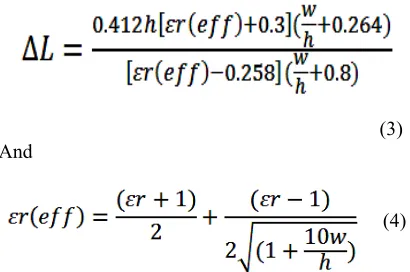
MOHAMMED B. MAJED
Department of Computer Science, College of Science and Technology, University of Human Development – Iraq
E-mail: [email protected]
ABSTRACT
Low profile antennas support the operation of many modern communication systems. Microstrip patch antennas represent one family of compact antennas that offer a conformal nature and the capability of ready integration with communication system's printed circuitry. And it has many advantages over conventional antennas. In this paper a square Microstrip Patch Antenna has been designed at 2.4 GHz frequency. By using Microwave office 2006 software (AWR) for design simulation to get the best parametric design, and compared with a slotted version of the antenna having a slotting shape of letter (P). It included in the design the return loss, gain, radiation pattern, bandwidth, HPBW, co and cross polar
isolation parameters. The square slotted antenna that designed has a result of a return loss is about ( - 42.41dB ) and about 12.92% bandwidth.
Keywords: Return Loss, Coaxial Feed, Bandwidth, Antenna Radiation Pattern, Co-Polar Isolation,
Cross-Polar Isolation.
1. INTRODUCTION
Microstrip antennas (MSAs) are used in a broad range of applications from communication systems to biomedical systems, primarily due to several attractive properties such as light weight, low profile, low production cost, conformability, reproducibility, reliability, and ease in fabrication and integration with solid state devices. In recent years the rapid decrease in size of personal communication devices has lead to the need for more compact antennas. As communication devices become smaller due to greater integration of electronics, the antenna becomes a significantly larger part of the overall package volume. Presently there are many other government and commercial applications, such as mobile radio and wireless communications that use microstrip antennas [1] [2].
[image:1.612.313.523.429.617.2]Microstrip antennas however have limitations in terms of bandwidth and efficiency, all imposed by the very presence of the dielectric substrate. The following drawing shows a patch antenna and its basic form: a flat plate over a ground plane, the center conductor of a coax serves as the feed probe to couple electromagnetic energy in and/or out of the patch [3].
Figure 1: Shows The Form Of The Microstrip Patch Antenna
feed lines are usually photo etched on the dielectric
substrate [4].
Microstrip patch antennas can be fed by a variety of methods. These methods can be classified into two categories-contacting and non-contacting [5]. In the contacting method, the RF power is fed directly to the radiating patch using a connecting element such as a microstrip line. In the non-contacting scheme, electromagnetic field coupling is done to transfer power between the microstrip line and the radiating patch. The four most popular feed techniques used are the microstrip line, coaxial probe, aperture coupling and proximity coupling [6].
In this paper more details mentioned to it such as the dielectric substrate dimensions, feeding contact point dimensions and also the slotted design in our letter (P), it depends on position & size of letter. And there is another thing also important the (positioning the feeding point), because when we want to get best RL result it must move feeding point randomly until getting a best results, and this is take a lot of time to get it.
2. DESIGN CONSIDERATION
[image:2.612.314.519.433.569.2]There are many things or parameters that should be putted in consideration before starting the design of microstrip patch antenna, like the length (L), width (W) and the thickness (h) of the patch and also Dielectric constant of the substrate (εr) and the Frequency of operation. And these parameters showed in figure 2.
Figure 2: The Parameters Of The Microstrip Patch
To start there are two important values in the design must be found, the Width and Length of the patch [7].
Firstly the width can found from the equation (1):
(1)
And the operating frequency (2.4) GHz is given and also the dielectric constant (4.7) that it needs to calculate the width (w).
It founded the width equals approximation: W=37 mm.
Then also must calculate the length, it can be found from the equation (2) [8]:
(2)
As seen in the above equation it needs to find ΔL
and ε reff (Effective dielectric constant), and they can be found from equations (3) and (4) [9].
(3) And
(4)
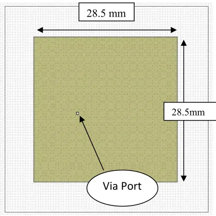
From equation (4) having (εr), so easily (ε reff) can be found, that equals 4.397, and then uses the last one in equation (3) to find ΔL that equals 0.731. After that to calculate the length (L) and it will be 28.5 mm.
It should also be mentioned that the thickness of the
air gap above the substrate is taken as 16mm which is well known as a practical value (10 times the thickness of the dielectric), and these dimensions have been chosen of the substrate to be
40mmX40mm, which is bigger than the patch, to
be enough, it used co-axial as afeeding technique.
And the dimensions of feed point is
0.5mmX0.5mm have been taken.
In the end after all these measurements, the un-slotted patch antenna designed and get the best
value of return loss is about (-42.8dB), after
[image:3.612.320.522.107.316.2]moving it randomly and at last get this value, as shown in figure 3.
Figure 3: Un-Slotted Patch Antenna
[image:3.612.90.305.280.495.2]Now design the slotted version of the same patch above, to implement the letter (P). And here in design also must change the shape of the letter and change it's position of course randomly until we get the best result. The design becomes as shown in figure 4.
Figure 4: Slotted Patch Antenna With Shape Letter (P)
After the slotted patch designed, the return loss and bandwidth must be computed. All of these computations for unslotted and slotted will show in simulation results.
3. SIMULATION RESULTS
Firstly it will show the simulation results of the un-slotted version. And then it will show the simulation results of the slotted version and compare between them.
The return loss for un-slotted design in the figure below:
Figure 5: Un-Slotted Patch Return Loss
28.5mm
28.5 mm
[image:3.612.314.524.551.696.2]From figure 5 above the bandwidth can be
calculated (BW) in -10dB RL in the lower & upper
frequencies f1 and f2. Upper frequency was
2.556GHz while the lower frequency was
2.245GHz and operation frequency was 2.4GHz. Firstly subtract f1 from f2 and the result divide it by square root of multiplying f1 and f2. And this gives the BW= 12.98%. As shown in Eq. below
BW = (f2-f1)/f
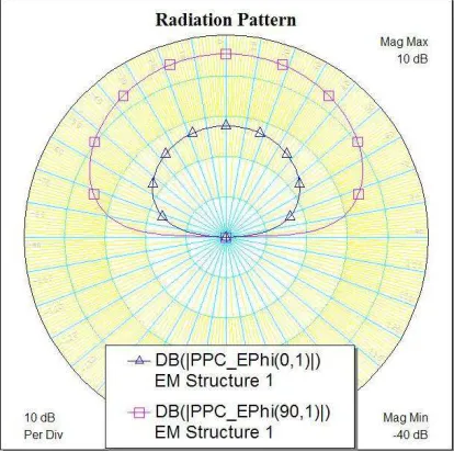
[image:4.612.314.522.199.368.2]Now from radiation pattern figure below, the other parameters can be calculated.
Figure 6: Un- Slotted Patch Radiation Pattern
The radiation pattern measured in term of (Phi) and θ (Theta). Because the radiation pattern is perpendicular to the patch.
And now the Gain calculated and it equals 4.634
dB. For calculating the HPBW (Half Power Beam Width) which is the maximum angle, and to
compute HPBW it should be dropped from 4.634
dB to 3dB gain and measure the angle from the top
to that position.
Ones in the right side and then in the left side and
add them. Founding HPBW has 66.86º, it gives
33.43º on each side, because the two sides are symmetrical.
And for the Co-Polar isolation is the same as the top value of what has E-Phi 90º value, which is
4.634 dB, while the Cross-polar isolation is
calculated by subtracting the top value of E-Phi 90º from the top value of E-Phi 0º which will be:-
4.634 dB – (-12.9 dB) = 17.534 dB
[image:4.612.91.298.270.476.2]Returning to slotted patch design, and compute the parameters as it had been done in un-slotted patch.
Figure 7: Slotted Patch Return Loss
From figure (7) above the bandwidth can be
calculated (BW) in -10dB RL in the lower & upper
frequencies f1 and f2. Upper frequency was
2.551GHz while the lower frequency was
2.242GHz and operation frequency was 2.4GHz. Firstly subtract f1 from f2 and the result divide it by square root of multiplying f1 and f2. And this
gives the BW= 12.92%. As shown in Eq. below
BW = (f2-f1)/f
Figure (8), Slotted patch radiation pattern
As obvious from figure above is approximately the same in slotted and un-slotted design. The Gain is
4.647 dB, the HPBW has 67.3º. And for the Co-Polar isolation is the same as the top value of what
has E-Phi 90º value, which is 4.647 dB. Cross-polar
isolation is calculated by subtracting the top value of E-Phi 90º from the top value of E-Phi 0º which will be:-
4.647 – (-12.8 dB) = 17.447 dB
4. ANALYSIS AND DISCUSSION
From the results in the slotted and the un-slotted design, as seen before by making slot on the patch and all results, all parameters almost the same as un-slotted. The performance of the antenna that designed not changed very high. And these results depend on the position and size of the slot (P), this position and size have been chosen randomly by trial and error. And every time changing them we get different results. And all results that got of course depend on the other parameters, like dielectric substrate, this must be chosen carefully. And the dimensions of the feeding point also important to choose it and not changed during simulation.
Now in radiation pattern seen in the figures that is no change or approximately the same, HPBW, the Co-Polar isolation and Cross-polar isolation. In the end the bandwidth BW changed but small decrease as mentioned.
5. CONCLUSION
A square microstrip patch antenna was designed at frequency 2.4 GHz. As seen in this paper in the results an important parameters included like feed network and impedance matching in microstrip patch antenna design. And also the affect of changing the position of feed point on the performance of the antenna. And a comparison has made between the un-slotted design and slotted one. And the results discussed if the size and position of letter (P) changed.
REFERENCES:
[1] Kin-Lu Wong, “Compact and Broadband
Microstrip Antennas”, John Wily & Sons,
2002.
[2] Bahl, I.J. and Bhartia, P., Microstrip Antennas, Artech House, Dedham, MA, 1990.
[3] R. B. Waterhouse, “Cross-polarization
characteristics of the circular patch antennas,” Electron. Lett., 1997.
[4] J. M. Laheurte, A. Papiernik, and J. R. Mosig, “Modeling of coaxial feed contribution to microstrip antenna impedance: Comparison of
a numerical model with analytical
expressions,” Int. J. Microwave Millimeter Wave CAE, 1993.
[5] N. Herscovici, “New Considerations in the
design of Microstrip Patch Antennas, IEEE
Tram’ on Antennas & Propagation, Vol. 46, June 1998.
[6] Ting-Hua Liu and Wen Xun Zhang, “Compound techniques for broadening the bandwidth of microstrip patch antenna,” Microwave Conference Proceedings, Dec. 1997
[7] Shakelford, A., Lee, K.F., Chatterjee, D. , Guo, Y.X. , Luk, K.M. , Chair, R. ,“Small-Size Wide-Bandwidth Microstrip Patch Antennas,”
Antennas and Propagation Society
International Symposium, July 2001.
[8] Behera, Subhrakanta, and Kalarickaparambil Joseph Vinoy. "Microstrip square ring antenna
for dual-band operation." Progress In
Electromagnetics Research 93 2009, 41-56. [9] Afridi, Muhammad Aamir. "Microstrip Patch
[image:5.612.92.329.74.296.2]