o
0
handbook
momoamB
o
handbook .
1972
Copyright
©
1972 by Digital Equipment CorporationDigital Equipment Corporation makes no representa-tion that the interconnecrepresenta-tion of its modular circuits in the manner described herein will not infringe on existing or future patent rights. Nor do the descrip-tions contained herein imply the granting of licenses to make, use, or sell equipment constructed in accord-ance herewith.
Digitai Equipment Corporation is not responsible for errors which may appear in the pricing, technical descriptions, illustrations, or photographs of the products appearing in this Handbook.
Digital Equipment Corporation reserves the right to make- substitutions and modifications in the specifica-tions of the products described in this Handbook.
Prices quoted are in U.S. dollars and apply to the United States only. The availability of products listed and the prices quoted herein are subject to change without notice.
FLIP CHIP, UNIBUS and OMNIBUS are trademarks of Digital Equipment Corporation,
This eighth edition of the LOGIC HANDBOOK is your guide to the most exten-sive line of products offered by Digital Equipment Corporation for implement-ing electronic logic designs for instrumentation, computer interfacimplement-ing, data gathering or control. This handbook is a basic reference for anyone involved in specifying, manufacturing or using solid state logic.
Our M Series TTL integrated circuit modules are featured in this edition. The M 'Series line consists of more than 100 modules ranging from basic and functional logic modules to self contained computer interfacing modules and the M Series Logic Lab for use in breadboarding M Series logic designs.
The impact of advancing technology can be seen in M Series evolution. From the beginning, M Series was TTL-integrated-circuit oriented; the current trend is toward MOS circuits, MSI and LSI. The result is more complexity (and more built-in design solutions) per module. Many of the modules in this handbook amount to full-scale digital subsystems. M1702, for example, is a complete 12-word input interface that plugs directly into the PDP-8/ e
or 81m OMNIBUS structure.
This edition of the handbook also covers the A Series of analog modules, the W Series of wire wrappable, collage and blank boards in the FLIP CHIP form factor, and a complete line of power supplies and hardware. An ex-panded section on cabling and cable accessories has been added to simplify system interconnection design. All these support functions provide a total capability for designing, implementing, and assembling a modular system, small or large, at the lowest cost per function in the industry.
In the historical modular concept conceived and perfected by DEC, innova-tion is balanced by performance and value, and the efficiency of highly complex, specialized modules is complemented by a full array of basic build-ing blocks. All tradeoffs and design decisions have been resolved by DIGITAL, giving the designer and manufacturer the freedom to concentrate on the best implementation of his control, instrumentation, or communications system.
Extensive non-catalog products and services are available from DIGITAL. If, you require unique functions that are not listed in this handbook, contact your local DEC office (listed inside the back cover). The product you need may be available as a non-catalog item. In addition, DIGITAL maintains a Special Module Products Group with complete capability of design, layout, manufacturing and test. Custom product capability is not limited to modules alone but extends to the support hardware and accessories, including cabling, wire wrapping and cabinets.
A worldwide staff of DIGITAL sales engineers is prepared to respond to your technical and commercial needs. From a backlog of -logic system design ex-perience, DIGITAL may have a detailed solution to your application or inter-face requirement.
Please address any comments on this handbook or inquiries concerning special services to:
. Digital Equipment Corporation 146 Main Street
Maynard, Massachusetts 01754
Foreword ... .,... iii
INTRODUCTION ... ... ... ... ... ... ... ... ... vii
Organization of Handbook ... ... vii
M Series Module Selector Guide ... viii
Digital Equipment Corporation Engineering Services ... viii
Special Symbols and Abbreviations ... viii
M SERIES LOGIC AND CONTROL MODULES ... 1
List of Modules ... 3
Standard Module Dimensions ... 5
Extended Module Dimensions ... 7
General Characteristics ... 8
Module Descriptions ... 27
M SER'IES MODULES FOR COMPUTER INTERFACING ... 119
OMNIBUS and, UNIBUS Interface Modules ... 121
OMNIBUS/UNIBUS Electrical Characteristics ... 122
External I/O Bus (Positive logic) ... 126
Negative Bus .... , . ... ... ... . .... ... .. ... ... ... 128
PDp·15 Bus ... 128
Module Descriptions ... 129
A SERIES ANALOG MODULES ... 225
Notes on Operational Amplifiers ... 227
2" and Resolution ... ... 234
Digital Codes for A/ D's, 0/ A's, and Data Acquisition Systems ... 235
Module Descriptions .. ~... 236
ACCESSORY MODULES ... 295
Wire Wrappable Module Boards ... 297
Collage Mounting Boards ... 303
Blank Modules ... ... 304
Module Extenders ... 308
Bus Connectors ... 311
POWER SUPPLIES ... ... 313
Power Supplies and Accessories Summary ... 314
CABLES AND ACCESSORIES ... 337
Standard Cables ... 339
Cable Connectors ... 349
I/O Connectors ... 370
HARDWARE ... 373
Connector Blocks ... 376
Mounting Panels ... 383
Module Drawers ... 394
Mounting Panel Frames ... 397
Cabinets ... 399
Wire Wrapping Service ... 418
Accessories ... 422
LAB SERIES ... 431
Computer lab ... 432
K Series logic lab ... 435
M Serie$ lab ... 443
ABOUT DIGITAL EQUIPMENT CORPORATION ... 447
General Description of DEC Products ... 450
Warranty Statement and Discount Schedule ... , ... 452
Product Index ... 453
ORGANIZATION OF HANDBOOK
This edition of the lOGIC HANDBOOK is organized in eight functional sec-tions for maximum ease of reference. Within each section, module descrip-tions are presented in alphanumeric order by module designation. To locate a specific module, consult the Product List at the end of the handbook.
Loeic and Control: This section includes all of the M Series basic logic mod-ules and those complex functional modmod-ules that are not computer-interface oriented. An introduction to this section describes the basic characteristjcs of the TTL integrated circuits which are the principal active elements of
M Series.
Computer Interfacing: This group includes the M Series complex function~
modules that simplify interfacing to the PDp·ll UNIBUS or PDP-S/e,
S/m
OMNIBUS. Also in this group are the modules for interfacing the external
1/0 bus of earlier PDP-S family computers plus level converters and other interface-oriented support modules. Introductory information defines the con-trol and data signals of the OMNIBUS, UNIBUS, and external I/O bus. Analog: The A Series of analog modules supports the M Series by providing a two-way translation between continuously varying real·world voltage mea-surements and the digital realm of control and computation. The present A Series emphasizes 10- and 12-bit performance in a family of mutually compatible functions-multiplexers, operational amplifiers, sample-and-hold circuits, D/ A and A/ [) converters, reference voltage sources and an expanded group of multiplying
0/
A converters.Accessory Modules: DEC offers a wide line of wire wrappable, collage, and blank modules in the FLIP CHIP form factor for experimenting and bread-boarding by users who want to work directly with discrete components and integrated circuit packages. Included in this section are module extenders and PDP-Sf e, 8/ m OMN IBUS bus connectors.
Power Supplies: This section describes a wide selection of Hand K Series dc power supplies for small and large systems. Summary tables are included that will help the system designer select the power supply appropriate to his system.
Cabling: This edition of the handbook presents a greatly expanded section on M and W Series cables and cabling accessories. DEC offers a complete line of prefabricated cables for interconnection of free-standing logic systems as well as computer-based installations. Bulk cable and cable cards are available so that the. user can design and contruct his own custom inter-connections with a minimum of custom design and planning.
Hardware: DEC makes a complete line of hardware accessories to support its module series. Module connectors are available for as few as one module to as many as 64 in a single 19u mounting panel. A complete line of
Lab Series: This group includes the COMPUTER LAB digital logic trainer, the
K Series logic lab (a rack-mounted, plugboard-panel breadboarding and
training facility for K Series modules) and the M Series logic lab (a console and rack structure that mounts and interconnects M Series modules for training, experimentation, and system design).
M SERIES MODULE SELECTOR GUIDE
Available as a companion to this handbook is the M Series Module Selector Guide, a pocket-sized chart that is used for a quick look-up of the charac-teristics of the M Series modules and the most important supporting hard-ware and accessories and power supplies in this handbook. Contact your local DIGITAL Sales Office for a free copy of the Module Selector Guide.
DIGITAL EQUIPMENT CORPORATION ENGINEERING SERVICES
In addition to supplying a complete line of standard and special hardware and accessories, Digital Equipment Corporation also provides an engineering, design and manufacturing service in support of customer applications. These services are available upon request and consist of the following:
Special logic Modules: Many of the same advanced manufacturing and test-ing techniques which DEC employs to produce its standard modules are applied to building special modules. DEC engineers can provide full module design and development services or they can work with user-supplied draw-ings and parts lists, depending upon user needs.
Wire Wrapping: Using the latest in automatic wire wrapping equipment, DEC can efficiently wire and check connector panels according to customer-supplied wire list and specifications.
Special Cables: When standard cables and cable lengths are not applicable to customer requirements, DEC offers a complete cable fabrication service to build special cables according to customer specifications.
Interface Design: DEC maintains a staff of experienced applications engi-neers who are capable of designing or providing design information for in-terfacing DEC computers to custom control systems and equipment.
Logic Arrays: Special-purpose logic systems can be efficiently designed and built from customer-supplied data_ DEC's capability extends from limited production system to high-volume production and insures both optimum design and high reliability at a reasonable cost to the customer.
SPECIAL SYMBOlS AND ABBREVIATIONS
• Logic symbols used in this handbook conform, in general, to widely accepted
Mil standards. All basic M Series logic symbols (AND, OR, NAND, NOR,
Inverter, Flip-Flop) are described in the introduction to the M Series togic and control modules.
Input loading and Output Drive
INPUT LOADING PIN NUMBER
It TTL UNIT LOADY(PINA,SIDEII
~:: ~_~"'::C1;.:..Fu'llW"l.OAOS'
ARROWS SHOW DIRECTION
[image:11.383.40.337.256.499.2]Of SIGNAL FLOW
Figure 1. logic Diagram Input loading and Output Drive Symbols
Bus DrIvers and Receivers
Drivers and receivers that transfer data along the bidirectional transmission lines of the PDP-8/e, 8/m OMNIBUS or the PDP-ll UNIBUS differ somewhat from similar TTL NAND gates or inverters. Typical examples are shown in Figure 2. The
"s"
in the loading box indicates that the driver or receiver circuit is to be connected to an OMNIBUS or UNIBUS signal or control line. In this application, unit loading need not be considered. "R" identifies a line receiver and "0" identifies a line driver. Inputs to line receivers or drivers may also be standard TTL levels, in which case, TTL unit loads are shown .as usual in the loading box.DATA TO BUS
B U2
DRIVE TO BUS
!!lBt •
~
1B R 7 GATED BUS
. RECEIVER
El 2
READ FROM BUS
DATA FROM BUS
TYPICAL BUS TRANSCEIVER ARRANGEMENT
Figure 2. Sus Driver and Receiver Symbols
Level Converters
Whenever logic levels are translated from one set of voltages to another, the conversion is shown taking place in a square level-converter symbol. Inside the box, the corresponding logic levels are related in a simple truth table. The example of figure 3 shows a level converter stage that accepts TIL levels (LOW and HIGH) and delivers DEC negative voltage levels (-3 V and ground).
Input loading is two TIL unit loads. Whenever loading is peculiar, it is de-fined in a note on the drawing as in the output of figure 3.
rzt02 _
n. _
01~
~
*'SINKS 20mA AT GROUNDfigure 3. Typical Level Converter
Special Analog Symbols
Symbols used on analog circuit drawings to represent multiplex switches and operational amplifiers are shown in figure 4. Loading boxes for analog inputs and outputs contain the letter "A"; do not connect such signals to logic levels.
MULTIPLEX SWITCH (MOS FET)
~
ALOGIC CONTROL INPUT
CONSTANT IMPEDANCE MULTIPLEX SWITCH
~---.
0
C~r-Y
INPUTOPERATIONAL AMPLIFIER
figure 4. Special Analog Symbols
Signal and Function Names
Inputs and outputs
of
M Series logic modules may be assigned a signal name, a function name, or both. (See figure 5.) Signal names appear out-side blocks or logic symbols to identify typical input or output signals. [image:12.385.35.339.256.502.2]_ - - - S I G N A L NAMES - -_ _ _ _ _ _
> - _ - - - + -___ -.:...~.~BTP3 H
I
~~·~I---~
INlnAUlE
H®~L---t-G>--I--~-f
·
~.'N'T
H .I
L-f:>o-+~BINIT
LI
(PART OF M1510)I
t-'--"-~lJ~~R L
~_~_<lUPL
ON H
~_----lENABLE H 1 AI COUNT IN H
J
(PART OF M236)
Figure 5. Signal and Function Names
Digital Equipment Corporation uses standard terminology to name signal lines to aid the reader in determining their active state. Either an H or l follows the signal name mnemonic, separated by a space. This letter indi-cates --the asserted (true) state of the signal. An H means the signal is as-serted when HIGH (+3 V) and an l means the signal is asas-serted when lOW (0 V). for example, a UNIBUS data line is called BUS 000 L and' a grant line is called BUS BG4 H.
On the logic diagrams of many computer interfacing modules in this hand-book, signal names peculiar to one computer, such as the PDP-II, appear as an example of typical usage. Signal names may be changed to those of another computer or interfacing device if logically appropriate.
function names appear inside the blocks of functional modules. They iden-tify the function of input or output signals. The user may add his own signal names.
Abbreviations
[image:13.383.35.310.63.316.2]ABBREVIATION ALTN AMPL ANLG BPS CAP CLR CMPR COM CONT CVRSN DAC EXT GND H INIT INT,INTR INTL L OUT P.1. POT PRGM REF RTN SER S.H. TRIG
Table I-Abbreviations
DEFINITION
Alternate
Amplifier
Analog
Bits Per Second
Capacitor Clear Compare Common Control Conversion
Digital to Analog Converter
External
Ground
High (TTL +3 V Logic Level)
Initialize
Interrupt
Internal
Low (TTL 0 V Logic Level)
Output
Program Interrupt
Potentiometer
Program
Reference
Return
Serial
Sample and Hold
[image:14.386.74.328.39.540.2]o
.
m~
logic and
M·SERIES LOGIC
AND CONTROL
MODULES
Modules in this section appear in numerical order. The six functional cate· gories of M·Serie, logic and control modules are:
MIll M112 MIl3 MIl5 M117 MIl9 M121 M133 M141 M160 M169 M610 MII03 M1307 GATES Inverters NOR Gates
NAND Gates NAND Gates NAND GATES NAND Gates AND/NOR GATES Input NAND Gates NAND/OR Gates AND/ NOR Gates Gating Module
Open Collector N'AN D Gates AND Gates
AND Gates
FlIP·FLOPS
M202 Triple J·K Flip·Flop
M203 8 R/S Flip-Flops
M204 General·Purpose Buffer & Counter
M205 General-Purpose Flip·Flops
M206 General·Purpose Flip·Flops
M207 General·Purpose Flip-Flops
M208 8·Bit Buffer/ Shift Register
M232 16·Word RAM
TIME RELATED
M302 Dual Delay Multivibrator
M306 Integrating One Shot
M310 Delay line
M360 Variable Delay
M401 Variable Clock
M403 RC Multivibrator Clock
M404 Crystal Clock
M405 Crystal Clock
M410 Reed Clock
M452 Variable Clock
M501 Schmitt Trigger
M521 K to M Converter
M602 Pulse Amplifier
M606 Pulse Generator
MI59 MI61 Ml62 Ml6S M230 M236 M237
M040 M050 M617 M627 M660 M661
M002 M261 M262 M706 M707 M906 M7390
NUMERIC
Arithmeticl Logic Unit
Binary to Octal Decimal Decoder Parity Circuit
12·Bit Magnitude Comparator
Binary to BCD & BCD to Binary Converter 12·Bit Binary Upl Down Counter
3·nigit BCD Upl Down Counter
LOGIC AMPLIFIERS
Solenoid Driver Indicator Driver
4·input Power NAND Gates NAND Power Amplifier Positive Level Cable Driver Positive Level Driver
MISCELLANEOUS
Logic HIGH Source 4·State Motor Translator IO·State Motor Translator Teletype Receiver Teletype Transmitter Cable Terminator
Asynchronous Transceiver
M Series modules contain high speed TTL logic in both general purpose and functional logic arrays. TTL was chosen for its high speed, capacitance drive capability, high noise immunity and choice of logical elements. High per· formance integrated circuit modules are now available at approximately one half the price of their discrete or hybrid counterparts.
STANDARD MODULE DIMENSIONS
SINGLE-WIDTH FLIP CHIP MODULE
CONDUCTIVE COMPONENT LIMIT 1~32
t
NONCONDUCTIVE~PO!i~T~
!/i
~x.
0.056"
~~~~======~SI~~~l~========i===~=a1-U
i
t
SIDE 2
It~ MAXIMUM HEIGHT OF SOLDERED ~ENT LEADS
GOLD-PLATED CONTACTS
ETCHED WIRING SURFACE
SINGLE-HEIGHT FLIP CHIP MODULE
~~-=-==-==--~-
-
-::==;:=:-r-'~"==;r;:-,~o ~
Sl~ 2
2.187*
~::::::::~--- 3.875*'---+--~
o
.045" ,080"
rlool ...
·72_5_"~
_ _ _ _ _ 5I~
_ _ _ _ 1/_8_T_ YP._'
-I.~I
~IOII""'--- 5~2
DOUBLE WIDTH FLIP CHIP MODULI
C
CONDJCTIVE COMPONENTLIM~::~
_ _ _ _ _ ...,27/32mox.
NONCONDUCTIVE COMPONENTS
''t6 MAXIMUM HEIGHT OF SOLDERED COMPONENT LEADS
SIDE 1
SI 2
GOLD-PLATED CONTACTS
ETCHED WIRING SURFACE
0.056
DOLSLE HEIGHT FIrIP CHIP MODULE
.----.080 .045
0.099
-;;:;:---
- - - -
---.,
==~~=~~==~!~
ADI
0AE
M I
AJ
~
I
2.240 :~
1
::
IAP
I
AR
.370
:!
~_~!~~~V
I
f f
... MAXIMUM USEABLE COMPONENT AREA
_ SlOE 2 •. 9
1
37*
!
ii...
3.87!5" ..I
:~
1
i
IP
~ I
iL _____ -____ _
____
1
0.725
~
~8
TYP,... - - - 5
Y64
EXTENDED MODULE DIMENSIONS
SINGLE-WIDTH FLIP CHIP MODULE
CONDUCTIVE COMPONENT LIMIT 1 ~32
~
NON CONDUCTIVE COMPONENTS0.056
~~~====~SI~DE~'~===t E=~~~$3LL~
f
=r
SIDE 2~t6
MAXIMUM HEIGHT OF SOLDERED COMPONENT LEADS0.099
GOLD-PLATED CONTACTS
ETCHED WIRING SURFACE
SINGLE-HEIGHT FLIP CHIP MODULE
-==+===:;===*==1;;;;;;;;:;;;;;;;;;:;
A - - --2~6 2.240
B
C
D
E
F
~ SIDE 2
K L M N
p
:
.
=r=;;;;Y;;. E"'===;::;;;T
=*=I:::::::::::::::Iu v _ _ _ _ _ _ _ _
__ Jo
.045
. oeo
I/e TYP.
I
...
---e~•
DOUBLE WIDTH FLIP CHIP MOOI..l.E
C
CONDUCTIVE COMPONENT LIMITS "".~---.
27/32 max.
NONCONDUCTIVE
COMPONENTS
~MAXIMUM HEIGHT OF
SOlDERED COMPONENT
LEADS
SIDE I
SIDE 2 GOLD- PLATED CONTACTS
ETCHED WIRING SURFACE
DOUBLE HEIGHT FLIP CHIP MODULE
r - - - - . 0 8 0 .045
0.099
~----==~=±=~====~!~
2.240
1
.370!
53/
16
f
f
AD AE AF At! AJ AK AL AM AN AP AR AS AT AU 8A B8 8e 80 :~
..
8H 8J 8K 8L 8M 8N BP aR as aT auSIDE 2
8~ _ _ _ _ _ _
o
o
~8
TYP. I. . . - - - - 8 ' / 2 II
. . MAXIMUM USEABLE
COMPONENT AREA
.080 .045
0.099
- - -
---,
0I
I
I
II
I
I
If
I
I
I
I
I
10.436 I
I
I10.t87*
I
SlOE 2
I
I
I
I
DA D8
DC I
I
DO
DE
OF
DH DJ
Ill( I
I
Dt.
OM DN DP
DR OS
DT
0
DU
DV _ _ _ _ _ _ _ _
0.099~
.1
*-
MAXIMUM USEABLE COMPONENT AREAGENERAL CHARACTERISTICS
M Series high-speed, monolithic integrated circuit logic modules employ TTL (transistor-transistor logic) integrated circuits which provide high speed, high fan out, large capacitance drive capability and excellent noise margins. The M Series includes a full digital system complement of basic modules which are designed with sufficient margin for reliable system operation at frequencies up to 6 MHz. Specific modules may be operated at frequencies up to 10 MHz. The integrated circuits are dual in-line packages.
The M Series printed circuit boards are identical in size to the standard FLIP CHIPTM modules. The printed circuit board material is double-sided pro-viding 36'pins in a single height module. Mounting panels (H910 and H911) and 36-pin sockets (HS03 and HSOS) are available for use with M Series modules. Additional information concerning applicable hardware may be found in the Power Supply & Hardware and Accessories section of this handbook.
M Series modules are compatible with Digital's K Series and, through the use of level converters, are compatible with all of Digital's other standard negative voltage logic FLIP CH IP (Ii) modules.
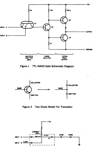
TIL NAND GATE
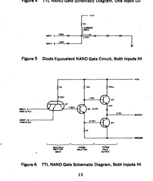
The basic gate of the M Series is a TTL NAND GATE. Figure 1 is the basic two input NAND gate schematic diagram. The circuit is divided into 3 major sections, the multiple emitter input, the phase splitter and the totem pole output circuit. The two diode model of a transistor shown in Figure 2 will be used in the analysis of the circuit. A forward biased silicon junction (Le. diode) gives a voltage drop of about 0.75 volts and a saturated silicon transistor has a collector emitter voltage of 0.4 volts average. These two figures will be used throughout the following discussion.
With either input at the La logic level (O.OV-O.SV) the multiple emitter input transistor will be ON with its base residing at about 0.75
+
0.4=
1.15 volts. The three diode string consisting of QI'S base collector diode, Q2'S base emit-ter diode, and Q/s base emitemit-ter diode will haye only 1.15 volts across it and will therefore be conducting only leakage currents (0.75+
0.75+
0.75=
2.25 volts required for forward bias). With no current flowing into ·the base emitter junction of Q2, the transistor will be OFF and its collector emitter voltage is alowed to rise. Similarly with no current flowing in the base emitter diode of Q4 the transistor is OFF and its collector emitter voltage is allowed to rise. When both Q2 and Q4 are OFF, QJ is freed to pull the output voltage to a HI level. The voltage levels present in the circuit with one or more lO. in-puts is shown in Figure 4.If both inputs are HI (2.4-3.6 volts) the head of the three diode string will re-side at about 2.25 volts and there will be a current path from the 4K base resistor on the input transistor through the diode string to ground as shown in Figure 5. With current flowing in the base emitter junctions of both Q2 and
~---,---,---+5V
Ql
INPUT A ----~_t:....~)'---_ti Q2
---~T
INPUT B - - - '
Q4
IK
~---~~---~
____
~~----J~~----~---J,\~----__
---J
MULnPLE EMITTER INPUT
PHASE
SPl..ITTER
TOTEM POLE OUTPUT
Figure 1 TTL NAND Gate Schematic Diagram
COUECTOR
lASE
I> eASE
EMITTER
Figure 2 Two Diode Model For Transistor
QUE Q48E
INPUT A ---~IO-""::'=~---*"-i----otf---4~---,
I
N"UT B (LOW) L.: _ _ _ _ _ _ _ _ _ .J t
[image:26.381.39.362.8.521.2]INPUT A HIGH INPUTB LOWIO.411)
4K 1.6K. 130 .... 03 3.511 04
______
---/~'---~--~MULTIPLE EMITTER
IfIIPIJT
PHASE
SPUTTER TOTEM POLE O\ITPUT
• !III
[image:27.381.22.331.193.557.2]OUTPUT
Figure 4 TTL NAND Gate Schematic Diagram. One Input LO
+ !ill
INPUT B ~HI;.:;GHc:..-IO-_ _ '"
Figure 5 Diode Equivalent NAND Gate Circuit. Both Inputs HI
INPUT A HIGH 12.4V)
INPUT B HIGHC2.4VI
4K I.GK I30A 03
0.4V 04
_______ ---/l~--..._---"~
MULTIPLE EMITTER INPUT
PHASE
SPUTTER
TOTEM POlE OUTPUT
+511
OUTPUT
OPERATING CHARACTERISTICS
Power Supply Voltage: 5 Volts ± 5%
Operating Temperature Range: 0° to 70°C
Speed: M Series integrated circuit modules are rated for operation in a sys-tem environment at frequencies up to 6 MHz. Specific modules may be oper-ated at higher frequencies as indicoper-ated by the individual module specifica-tions.
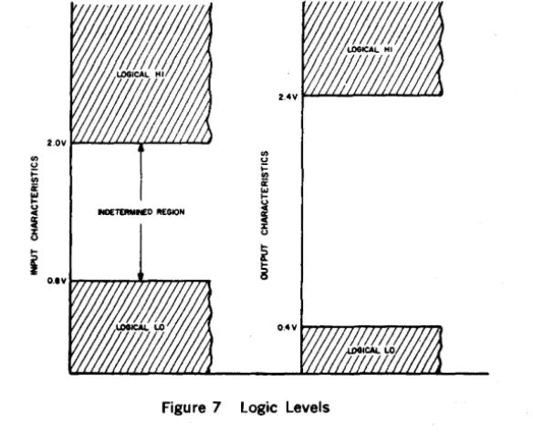
LOGIC LEVELS AND NOISE MARGIN
A gate input will recognize 0.0 volts to 0.8 volts as logical LO and 2.0 volts to 3.6 volts will be recognized as a logical HI. An output is between 0.0 volts and 0.4 volts in the logical LO condition. The logical HI output condition is between 2.4 volts and 3.6 volts. Figure 7 shows diagrammatically the accept-able transistor-transistor logic levels. The worst case noise margin is 400 millivolts that is, an output would have to make at least a 400 millivolt excur· sion to cause an input which is connected to it to go into the indetermined voltage region. For instance if an output were at 0.4 volts (worst case logical LO) there would have to be a
+
400 mv swing in voltage to cause inputs connected to it to go into their indetermined region.Input and Output Loading: The input loading and output drive capability of M Series modules are specified in terms of a specific numDer of unit loads. Typically the input loading is one unit, however certain modules may contain inputs which will, present greater than one unit load. The typical M Series module output will supply 10 unit loads of input loading. However, certain module outputs will deviate from a 10 unit load capability and provide more or less drive. Always refer to the individual module specifications to ascer· tain actual loading figures.
Unit Load: In the logic 0 state, one unit load requires that the driver be able to sink 1.6 milliamps (maximum) from the load's input circuit while main· taining an output voltage of equal to or less than +0.4 v(!)lts. In the logic 1 state, one unit load requires that the driver supply a leakage current 40 microamps (maximum) while maintaining an output voltage of equal to or greater than +2.4 volts.
Figure 7 logic levels
NAND Logic Symbol: logic symbology used to describe M Series modules is based on widely accepted standards. logic symbols and a truth table for the NAND gate are shown in Figure 8.
A~-OUTPUT
B~A.B
A~
O'-lTPUTB~i+B
AL L
H
H
B OUTPUT
L H
H H
L H
[image:29.384.48.340.23.260.2]H L
Figure 8 NAND Gate logic Symbol and Truth Table
The first symbol is visually more effective in applications where two high in-puts are ANDed to produce a low output. The second symbol better repre-sents an application where low inputs are ORed to produce a high output.
TTLAND/NOR GATE
r---~----_1---._---_O +vcc
A
B
C
D
. _ - -... _ 0 OUTPUT
Figure 9 TTL AND/NOR Gate Simplified Schematic
Circuit Operation: The basic elements of the TTL NAND gate are used with-out modification. The phase-splitter (Q2) is paralleled with an identical transistor (Q6), also controlled by multiple-emitter input transistor which receives two additional inputs, C and D. When either of the input pairs are high, the phase inverter operates to switch the output voltage low_ Circuit performance is essentially identical to the TTL NAND circuit.
AND/NOR logic Symbol: The logic symbols for the AND/NOR gate are shown and defined in Figure 10.
:~OUTPUT
c AB+CD
D
A B C 0 OUTPUT
H I H ANY L
ANY H H
L 'H L H
L H H L H
H, L H L
H L L H
A~
8
OUTPUT ~ IA+B1IC +01
Figure 10 AND/NOR Gate logic Symbols and Truth Table
:~OUTM
:=D-
OUTPUTANDI NOR INPUTS TIED RESULTING NOR SYMBOL
Figure 11 NOR Connection of AND/NOR Gate
NAND GATE FLlP·FLOPS
RS Fllp·Flop: A basic Reset/Set flip-flop can be constructed by connecting two NAND gates as shown in Figure 12.
S E T - - - Q
PREVIOUS INPUT
RESULT STATE CONDITION
1 0 SET RESET 1 0
L H L H H L
H L H L L H
L H H H NO CHANGE H L H H NO CHANGE H L L H NO CHANGE
o
L H H L NO CHANGE RESET---QL H L L H H*
H L L L H H*
Ambiguous state: In practice the input that stays low longest will assume control.
Figure 12 RESET/SET NAND Gate Flip-Flop
CLOCKED NAND GATE FLlp·FLOPS
The Reset-Set flip-flop can be clock-synchronized by the addition of a
two-input NAND gate to both the set and the reset two-inputs_ (See Figure 13.) One of the inputs of each NAN 0 is tied to a common clock or trigger line.
SET
CLOCK
o
RESET
A change of state is inhibited until a positive clock pulse is applied. The ambiguous case will result if both the set and reset inputs are high when the clock pulse occurs.
M SERIES GENERAL·PURPOSE FLlp·FLOPS
Two types of general-purpose flip-flops are available in the M Series, both of which have built·in protection against the ambiguous state characteristic of NAND gate flip·flops.
FLlP·FLOP CLOCK INPUT SYMBOLS
The D type flip-flop is a true leading (positive going voltage) edge triggered flip·flop and the D input is locked out until the clock input returns to low. The symbol to indicate this function will be as follows;
o
TYPE FLIP FLOP CLOCKThe operation of the J-K type flip-flop is to transfer the information present at the J and K inputs just prior to and during the clock pulse to the master flip·flop when the threshold is passed on the leading (positive going voltage) edge of the clock pulse. The information stored in the master flip-flop is transfered to the slave flip·flop. and consequentially to the outputs, when the threshold is passed on the trailing (negative going voltage) edge of the clock ~ulse. The symbol to indicate this function will be as follows;
J K TYPE FL I P FLOP CLOCK
o
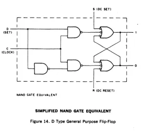
Type F1ip·Flop: The first of these is the D type flip-flop shown in Figure 14/ In this element, a single-ended data input (D) is connected directly to the set gate input. An inverter is provided between the input line (D) and the reset input. This ensures that the set and reset levels cannot be high at the same time.,---D---~---~
(SET)
C - - - - + - - - + (CLOCK)
I
I
I
I
L_
NAND GATE EQUIVALENT
$ (DC SET)
--,
>---+-~-O
I
_ ___ --.J
R (DC RESET!
SIMPLIFIED NAND GATE EQUIVALENT
Figure 14. D Type General Purpose Flip-Flop
The flip-flop proper employs three-input NAND gates to provide for de set ard reset inputs.
D type flip-flops are especially suited to buffer register, shift register and binary ripple counter applications. Note that D type devices trigger on the leading (or positive going) edge of the clock pulse. Once the clock has passed threshold, changes on the D input will not affect the state of the flip-flop due to 8 lockout circuit (not shown).
[image:33.380.36.327.40.322.2]"MASTER·SLAVE J·K FLlp·FLOP"
The two unique features of a J-K flip-flop are: A) a clock pulse will not cause any transition in the flip-flop if neither the J nor the K inputs are enabled during the clock pulse, and B) if both the J and the K inputs are enabled during the clock pulse, the flip-flop will complement (change states). There is no indeterminate condition in the operation of a J-K flip-flop_
A word of caution is in order concerning the clock input. The J and K inputs must not be allowed to change states when the clock line is high, the output will complement on the negative going voltage transition of the clock. It is for this reason that the clock line must be kept .Iow until it is desired to transfer information into the flip-flop and no change in the states of the J
and K inputs should be allowed when the clock line is high.
The J-K flip-flops used are master-slave devices which transfer information to the outputs on the trailing (negative going voltage) edge of the clock pulse. The J-K flip-flop consists of two flip-flop circuits, a master flip-flop and a slave flip-flop. The information which is present at the J and K inputs when the leading edge threshold is passed and during the clock high will be passed to the master flip-flop (The J and K inputs must not change after the leading edge threshold has been passed). At the end of. the clock pulse when the threshold of the clock is passed during the trailing (negative going voltage) edge, the information present in the master flip-flop is passed to the slave flip-flop_ If the J input is enabled and the K input is disabled prior to and during the clock pulse, the flip-flop will go to the "1" condition when the trailing edge of the clock occurs. If the K input is enabled and the J input is disabled prior to and during the clock pulse, the flip-flop will go to the "0" condition when the trailing edge of the clock pulse occurs. If both the
J and K inputs are enabled prior to and during the clock pulse, the flip-flop will complement when the trailing edge of the clock pulse occurs. If both the J and K inputs are disabled prior to and during the clock pulse, the flip-flop will remain in whatever condition existed prior to the clock pulse when the trailing edge of the clock pulse occurs.
J INPUT - - - + - - f
t OUTPUT
CLOCK
o OUTPUT K INPUT - - t - - - ;
Figure 16 shows a functional block diagram of 8 master slave J-K flip-flop using NAND gates. Gates C and D are the master flip-flop. Gates' G and Hare the slave flip-flop. Gates A and 8 are the steering •. network of the master flip-flop and the steering network for the slave flip-flop is comprised of gates E, F, and 1. The 1 output of the master flip-flop is point X. The operation of the flip-flop will be studied by examining the "I" to "0" transition of the flip-flops, with both the J and the K inputs enabled with a HI level before the clock pulse. When the leading edge of a HI clock pulse occurs, gate B wi" be enabled with three HI inputs. This will provide a RESET signal for t~e master flip-flop which will then go to the ~'O" condition. The slave flip-flop remains in the "1" condition while the clock pulse is HI because gate I is providing a LO signal to both gates E and F, thereby blocking inputs to the slave flip-flop. When the trailing edge of the clock pulse occurs, gate F will be enabled with a HI level at both its inputs and a RESET signal will be provided to the slave flip-flop, which will then go to the "0" condition. The next clock pulse, with both the J and K enabled, would cause the master flip-flop to go to the "1"
condition on the leading edge of the clock pulse and cause the slave flip-flop to go to the "1" condition on the trailing edge of the pulse. Figure 16 is a truth table for the J-K flip-flop showing all eight possible initial conditions_
INITIAL CONDITIONS FINAL CONDITIONS OUTPUTS INPUTS OUTPUTS
1 0 J K 1 0
L H L L L H
L H L H L H
L H H L H L
L H H H H L
H L L L H L
H L L H L H
H L H L H L
H L H H L H
UNUSED INPUTS (GATES AND FLfP·FLOPS)
Since the input of a TTL device is an emitter of .a multiple-emitter transistor, care must be exercised when an input is not to be used for logic signals. These emitters provide excellent coupling into the driving portions of the circuit when left unconnected. To insure maximum noise immunity, it is necessary to connect these inputs to a source of Logic I (High). Two methods are recommended to accomplish this:
1. Connect these inputs to a well filtered and regulated source of +3 volts. Pins UI and VI are provided on the MIl3, MIl7, M1l9, M121, M617, and M627 for this purpose.
2. Connect these inputs to one of the active inputs on the same gate. This results in a higher leakage current due to the parallel emitters and should be considered as an additional unit load when calculating the loading of the driving gate.
Connection of unused inputs to the supply voltage, Vcc, is not advisable, since power supplies are subject to transients and voltage excursions which could damage the input transistor.
TIMING CONSIDERATIONS
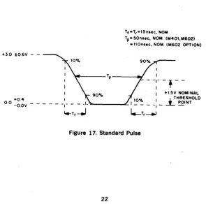
Standard Timing Pulse: In digital system design, a reference for system timing is usually required. The M Series modules M401 or M405 produces a standard pulse which provides such a reference. The standard pulse derived from each of these two modules is shown in Figure 17.
+3.0 j:O.6V -
-Tf- T,.15nsee. NOM.
Tp.50nsee, NOM. (M401,M602) -ll0nsee. NOM. (M602 OPTION)
I
... - -_ _ Tp _ _ _ ... " I
-
-:-
-
,
-
-I +1.5V NOMINAL
+0.4 I 10% I J. THRESHOLD
00 -O.OV - - - -,- - - .I- _ _ _ _ _ L 1 _ _ _ _ , _ - L POINT
~Tf...J
l.-Tr~
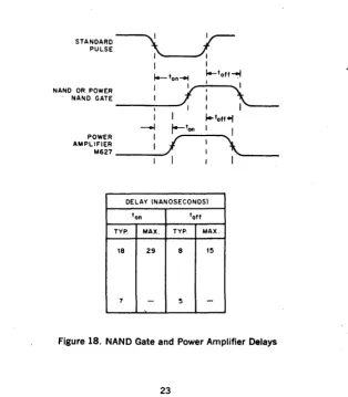
[image:36.381.38.334.263.555.2]NAND Gate and Power Amplifier Propaptlon Delays: The standard pulse (Figure 17) is distributed throughout a system in negative form to maintain the leading edge -integrity. (Since the TIL gate drives current in the logic
o
state, the falling edge is more predictable for timing purposes.) However, the standard pulse is of the wrong polarity for use as a clocking input to the type D and J·K flip-flops, requiring the use of a local inverter. Ordinarily, a NAND inverter is adequate. Where high fan-out is necessary, a M617 Power NAND is preferred.For applications requiring both high fan-out and critical timing the M627 Power Amplifier is available. This module contains extremely high-speed gates which exhibit turn-on times differing by only a few nanoseconds.
Simultaneity is desirable in clock or shift pulses distributed to extended shift registers or synchronous counters.
Delays introduced by inverting gates and power amplifiers are iUustrated in Figure 18. (Delays are measured between threshold points.)
STANDARD I
PULSE
NAND OR POWER NAND GATE
POWER AMPLIFIER
M627
I I
I I
le-ton----t I-toff~
I I_~-.... I I
--I
r-ton
:;
I
I
j.toff-i
I
I
,--
I
DELAY (NANOSECONDS)
ton toft
TYP. MAX. TYP. MAX.
1e 29 e 15
7
-
5-Figure 18_ NAND Gate and Power Amplifier Delays
[image:37.379.32.346.192.550.2]Flip-Flop Propagation Delays: D type flip-flops trigger on the leading or rising edge of a positive clock pulse; the propagation delay is measured from the threshold point of this edge. The set-up time of the D flop is also measured from this threshold point. Data on the D input must be settled at least 20 nanoseconds prior to the clock transition. The advantage of the D-flip-flop. however, is that the leading edge triggering allows the flip-flop AND gates to propagate while the clock pulse is still high. Figure 19 illustrates this situa-tion_
CLOCK
o TYPE FLIP FLOP
'-20 ... I·...---NS50EC~ I NSEC I
I ~~T I I
I I I
I +
I
I I
t---30----.t NSEC I
OUTPUT _ _ _ _ _
Figure 19. D Type Flip-Flop Timing
JK type flip-flops are, in effect, trailing edge triggering devices as explained previously. The only restriction on the J and K inputs is that they must be settled by the time that the rising edge occurs_ Timing is shown in Figure 20.
!..---J
AND K INPUTS MUST BE I STABLE BY THIS TIME ITRIGGER
PULSE
___ 1
\
----FLIP- FLOP OUTPUT
I
-.1
I
l.-
I_ _
y
Figure 20. J-K Flip-Flop Timing
[image:38.379.33.332.330.538.2]When using the dc Set or Reset inputs of either flip-flop type, propagation delays are referenced to the falling edge of the pulse. This is due to the inverted sense of these inputs. When resetting ripple type counters (where the output of one flip-flop is used as the trigger input to the next stage) the reset pulse must be longer than the maximum propagation delay of a single stage. This will ensure that a slow flip-flop does not introduce a false transi-tion,. which could ripple through and result in an erroneous count.
One-Shot Delay: Calibrated time delays of adjustable duration are generated by the M302 Delay Multivibrator. When triggered by a level change from a logical one to a logical zero, this module produces a positive output pulse that is adjustable in duration from 50 to 750 nsec with no added capacitance. Delays up to 7.5 milliseconds are possible without external capacitance. (See M302 specification.) Basic timing and the logic symbol are shown in Figure 21. The 100 picofarad internal capacitance produces a recovery time of 30 nsec. Recovery time with additional capacitance can be calculated using the formula;
OUTPUT (TYPICAL)
tr Nanoseconds
=
30 C Total (Picofarads) 100~
D
0.5.~
OUTPUTI I
L-1I-.J
LOGIC SYMBOL
I I
f4--
tr - - - . :, I
I
,
I
I I
---'1 i4--50 nsec TYPICAL I
,
jf'
: : 4 - ---~-':'
50 TO 750 nsec ____.__J,.
, I, TIMING
Figure 21. One-Shot Delay Timing and Logic Symbol
SYSTEM OPERATING FREQUENCY
[image:39.380.31.342.182.500.2]1. A standard clock pulse width of 50 nsec is assumed. This period is measured from the threshold point of the leading edge to the threshold pOint of the trailing edge.
2. One flip·flop propaga~ion delay of 35 nsec from the trailing edge of the clock pulse to the threshold pOint of the final state of the flip-flop is allowed.
3. Two gate-pair delays of 30 nsec each are assumed. (A gate-pair consists of two inverting gates in series.) Two gate-pair delays are usually re-quired to perform a significant logic function with a minimum of parallel operations. The two ga~e-pair delays total 60 nsec. '
[image:40.381.41.339.181.448.2]The time necessary to perform these operations before the next occurrence of the clock pulse is the sum of the delays; 50
+
35+
60, or 145 nsec. AII9W-ing 20 nsec for variations within the system, the resultAII9W-ing period is 165 nsec, corresponding to a 6 MHz clock rate. This timing is demonstrated in Figure 22.GATE GATE CLOCK F/F PAIR PAIR WIDTH DELAY DELAY DELAY IDLE
t -
n~
- t - -n~c
...n!~
...n!~c ~
n~~c--i
I I I I I I
I I I I
CLOCK
o
JK FLIP - FLOP
j
0---GATE PAIR 1
j
0---_ 0---_0---_0---_0---_
I:
GATE PAIR 2 .
o
Figure 22. Delays Determining System Operating Frequency
Substitution of a D type flip·flop results in a similar timing situation. In a system using both D and J-K flip-flops, note that the D flip-flop triggers on the leading edge of the clock pulse and the J-K flip-flop triggers on the trailing edge. When calculating system timing using D flip-flops, remember that the flip-flop inputs must be settled at least 20 nsec prior to the occurrence of the clock pulse.
M002
,
LOGIC HIGH SOURCE
Length: Standard Height: Single
Width: Single
+3V
SOURCE
Volts
+5 GND
Power mA (max.)
16
Pins
A2
C2. T1
MISCELLA-NEOUS
M SERIES
Price:
$10
I
M040
SOLENOID DRIVER
Length: Standard Height: Single
Width: Single
-v
o
-v
Volts+5
GND -15o
Power mA (max.) 47 9LOGIC
AMPLIFIERS
M SERIES
LOADS
---,
Price:
$39
---t-'l
_ _ _ ...II I
+r' - - - , - I
10-
-I
P~
I--_...J
~ L~.!.J
Pins A2
C2. Tl
82
The M040 contains two identical high-voltage driver circuits. Each consists of a 4-input positive NAND gate that controls a PNP transistor switch. The switch is capable of sinking up to 600 rna of current from an external power supply of up to -70 volts. One terminal of the load device (relay, etc.) must be connected to the external voltage, the other to the driver output. The positive terminal of the external supply connects to the module ground.
APPLICATIONS
The M040 can drive relays, solenoids, stepping motor windings and similar inductive loads.
Restrictions: Not recommended for
Indicator drive 115 V ac applications Logic level conversion
..
FUNCTIONSON Condition: Each driver sinks current from the external circuit when all four control inputs are HIGH. The amount of current is determined by the external voltage and load impedance. (The internal switch is a saturated PNP transis-tor.) Typical output voltage when sinking 0.6 A is -2 volts.
Anti-Kickback: Pin V2 of the driver module must be connected to the external supply so that the drivers will be protected from the back voltage generated by inductive loads. If the wire to the power supply is more than three feet long, it may have to be bypassed at the module with an electrolytic capacitor to reduce the pulse overshoot caused by the inductance of the wire.
Improving Recovery Time: If pin V2 is connected to the supply through a re-sistor, the recovery time of inductive loads can be decreased at a sacrifice in maximum drive voltage capability. Maximum rated supply voltage less actual supply voltage should be divided by load current to find the maximum safe resistance. When both circuits on a module are used, the load current for the above calculation is the sum of the currents.
PRECAUTIONS
Grounding: High current loads should be grounded directly at pin C2 of the M040, rather than at a frame or .bus ground.
Parallel Operation: No more than two circuits should be paralleled to drive loads beyond the current capabilities of single circuits.
SPECIFICATIONS
Current sinking capability: 600 mA per circuit, max.
External supply Yoltage: 70 V dc max.
Circuit Delay: Typical propagation delay for each circuit is 5 p'S (between
M050
AMPLIFIERS
LOGIC
50 MA INDICATOR DRIVER
Length: Standard Height: Single
Width: Single
2 +3 -v 01
2
*
o 0
~
L:.J - ~ - I.::.J
~
~. U-.~ L!!.J
2 +3 -v Rl
2
*
o
0M SERIES
Price:
$31
2 +3 -v L1 2 +3 -v El
2
*
2*
o 0 - 0
~
2 +3-V F12
*
o 0
2 +3 -v P1.
2
*
o 0
2 +3 -v Kl
2
*
o 0
* .
50 MA, -30V MAX.Volts
+5
GND
-15
Power mA (max.)
47 16 Pin A2 C2 82
~
~-~ ~+3 -v Jl
2 o 0
*
2 +3 -v 51
2
*
o 0
The M050 contains twelve transistor inverters that can drive miniature in-candescent bulbs such as those on an indicator panel.
APPLICATIONS
The M050 is used to provide drive current for a remote indicator, such as Drake 11-504, Dialco 39-28·375, or Digital Indicator type 4908, or as a level converter to drive 4917 and 4918 indicator boards.
Restrictions: Do not use to drive inductive loads (relays, solenoids). Note: For those applications requiring the sinking of current, refer to K Series.
fUNCTIONS
A LOW level on the input of the driver causes current to flow in the output.
SPECIFICATIONS
Length: Standard Height: Single Width: Single
Mill
INVERTER
Volts
+5
GNDPower mA (max.)
87 A2 Pins
C2, T1
Sixteen Inverters with input! output connections as shown.
APPLICATIONS
• Output Expansion • Logical Inversion
GATES
M SERIES
Price:
length: Standard Height: Single
Width: Single
Ml12
NOR GATE
~
AICl,O
1 8t
~
DlFl 10 t 1
~
DZF2 '0
1 E2
Kt
~
Ht1 J1 10
~
HZK2 t
t JZ
Power
GATES
M SERIES
Price:
$35
~
lZN2 '0 1 M
51
~
P1 .1 R1 10
~
P2 52RZ 1 1 :
~
TZ ., V2
,0
t UZ
+3V
I ::::
Volts
+5
GND
mA (max.)
50
Pins
A2
C2, T1
The M112 contains ten positive NOR gates. each performing the function A
+ B. Pins UI and VI provide two separate logic HIGH sources (+3V) each capable of holding up to 40 unused M Series inputs HIGH.
~
.M113, MIlS, M117, Ml19
NAND GATES
GATES
Length: Standard Height: Single
Width: Single
Power
M SERIES
Price: MI13-$IB MI15-$IB MI17-$19
"Ml19-$lB
Volts
+5
+5
+5
+5
GND
mA (max.) 71 M113 41 M115 41 M117 19 M119
Pins A2 A2 A2 A2
C2. T1
~
CI '0I B1
~
1M!~
FI '0t EI
~
~
FZ toI E2
. SI '0
~
I R'~
KI 10~
. S2t JI 1 R2 t
~
. K2~
tO V2
t J2 ,U2
M113 2-INPUT NAND GATES
S
1 ClE3
t F2E3
' K21 2
S
1 Ll1 Mt
~
1 R2E=i
' Rlt 51
M1t5 3-INPUT NAND GATES
M119 8-INPUT NAND GATES
These modules provide general-purpose gating for the M Series, and are most commonly used for decoding, comparison, and control. Each module per-forms the NAND function (A· B· C - - - N ) , depending upon the number of inputs.
APPLICATIONS
~ Logic gating
FUNCTIONS
M1l3-Ten two-input NAND gates that also may be used as inverters_ MIlS-Eight, three-input NAND gates.
MIl7-Six, four-input NAND gates.
MIl9-Three, eight-input NAND gates.
Unused inputs on any gate must be returned to a source of logic HIGH, for maximum noise immunity. In the M1l3, M1l7, M1l9, MI2I, M6I7 and M627 modules, two pins are provided (UI and VI) as source of +3 volts for this purpose. Each pin can supply up to 40 unit loads. MI03, MIll and M002 provide additional sources of logic HIGH level.
SPECIFICATIONS
M121
AND/NOR GATE
Length: Standard Height: Single
Width: Single
Volts
t~D
Power mA (max.)
50 Pins A2
C2. T1
GATES
M SERIES
Price:
$23
The M121 module contains six AND/ NOR gates which perform the function (AB
+
CD). By proper connection of signals to the AND inputs, the exclusive OR, coincidence, and NOR functions can be performed.APPLICATIONS
•
• Logic Gating
SPECIFICATIONS
,
MI33
TWO·INPUT NAND GATES
GATES
Length: Standard Height: Single
Width: Single
~
A1C1 10 1 B1
Ft
~
Dt1 E1 10
F2
~
D21 E2 '0
~
H'K1
to
, JI
~
H2. K2,O
1 J2
Volts
+5
GND
Power mA (max.)
160
M SERIES
Price:
$27
~
L1Nt 10
t M
~
l2 N2M2 W
1
~
P'S1 10
1R1
~
P2S2 '0
, R2
Pins A2
C2, Tl
This module provides general-purpose high-speed NAND gating.
APPLICATIONS
The high-speed characteristic of these gates frequently will solve tight timing problems in complex systems.
SPECIFICATIONS
Maximum output propagation delay to a logic HIGH or LOW is 10 ns.
Unused inputs on any gate must be returned to a source of logic HIGH for maximum speed and noise immunity.
Length: Height: Width:
M141
NAND/OR GATES
Standard Single Single
HIV
1.51<
Volts
+5
GNDPower mA (max.) 117
+5V
UK
Pins A2
C2. T1 ~U2
t V2
GATES
M SERIES
Price:
$29
+5V
t.5K
+5V
~r----~]~~--~:~~-- AB+CO+EF
By using one of the two inverters provided, a true AND/OR function can be realized. A maximum of four groups of gates can be connected together. Connection is made by merely connecting output pins together.
APPLICATIONS
• logic Gating
FUNCTIONS •
The M141 NAND/OR gate performs two levels of logic. The first is the NAND function which is identical to the M113 NAND gate. The second level is that of a wired OR for low logic levels. The two·input NAND gate which is used in the M141 does not have the standard TIL output circuit, but only the lower half of the totem pole output. This allows the outputs of these gates to be connected together and to share a common pun·up resistor.
SPECIFICATIONS
Propagation Delay: 70 ns max.
Vnlts
+5
<aNDPower mA (max.)
150
*=OPEN COLLECTOR-DRIVES 10 UNIT LDADS LOW
Pins A2
C2. T1
The M159 is fully cascadable. The CARRY OUT of the less significant M159 should be connected directly to the CARRY IN of the next more significant M159. The CARRY PROPAGATE and CARRY GENERATE output should be used with a carry look-ahead module or left unconnected.
The COMPARE output goes High whenever all the "F" outputs go High. This output is open-collector so that it can be wire-AND connected when M159 modules are cascaded. An example of how thisoutput can be used is shown
in the table below. .
When the arithmetic operation A minus B minus 1 is selected, the M159 can be used as a comparator.
A and B COMPARE CARRY
Data Inputs Output OUT
A>B 0 0
A
=
B 1 1A<B 0 1
[image:55.383.25.336.289.540.2]The maximum propagation delay ·from the "AN'" or "BN" bit input to the output bit "FN" in the logic mode is 48 nsec. which does not change as M159's are cascaded. In the arithmetic mode, the maximum delay from the "A" or "B" word input to the "F" word output, CARRY OUT, or COMPARE . is 50 nsec. which increases by 19 nsec. per additional cascaded M159 when carry look-ahead is not used. When carry look-ahead is used, the maximum additional delay is limited to 20 nsec. for up to three additional M159's.
Table of Logic Mode Operations
(MODE Input
=
1) (CARRY IN has no affect on Logic Mode Operations)Function NOTE that FN is com
pie-mented when the Function Selection Code is
comple-SELECTION CODE mented
53 52 51 50 Bit FN ~quals Bit F~ Equals
0 0 0 0 AN AN
0 0 0 1 AN AND BN AN OR BN
0 0 1 0 AN AND BN AN OR BN
0 0 1 1 0 1
0 1 0 0 AN OR BN AN AND BN
0 1 0 1 BN BN
(AN AND BN) (AN AND BN)
0 1 1 0 OR OR
(AN AND BN) (AN AND "BN)
0 1 1 1 ~ AND 'BN AN OR BN
Complemented Function
SELECTION CODE
S3 S2 SI SO
1 1 1 1
1 1 1 0
1 1 0 1
1 1 0 0
1 0 1 1
1 0 1 0
1
9
0 1S3
0
0 0
0 0 0 0
0 1 1 1 1 1
[image:56.386.33.351.35.447.2]1 1 1
Table of Most Useful Arithmetic Mode Operations
(MODE .nput =0)
Function Word F Equals
SELECTION CODE CARRY IN
=
1 CARRY IN=
052 SI 50
0 0 0 ,WORD A WORD A plus 1
0 0 1
0 1 0
0 1 1 Minus 1 (2's Comp.) ZERO
1 0 0
1 0 1
1 1 0 A Minus B Minus 1 A Minus B
1 1 1
0 0 0
0 0 1 A plus B A plus B plus 1
0 1 0
0 1 1
1 0 0 A Times 2 A Times 2 plus 1
1 0 1
1 1 0
S3
0
0 0
0
0 0
0
0 1
1
1
1
1
1 1
[image:57.385.11.341.39.448.2]1
Table of less Useful Arithmetic Mode Operations
(MODE Input
=
0)Function Word F Equals
SELECTION CODE
CARRY IN
=
1 CARRY IN=
0S2 S1 SO
0 0 0
0 0 1 A OR B A OR B plus 1
0 1 0 A OR
B
A OR 8 plus 10 1 1
1 0 0 A plus (A AND B) A plus (A AN 0 B) plus 1
1- 0 1 (A OR B) plus (A AND S) (A OR B) plus (A AND B)
plus 1
1 1 0
1 1 1 (A AND
B)
minus 1 A AND B0 0 0 A plus (A AND B) A plus (A AND B) plus 1
0 0 1
0 1 0 (A OR
B)
pIlls (A AND B) (A OR B) plu~ (A AND B)plus 1
0 1 1 (A AND B) minus 1 A AND B
1 0 0
1 0 1 (A OR B) plus A (A OR B) plus A plus 1
1 1 0 (A OR
B)
plus A (A OR B) plus A plus 1M160
ANDtNOR GATE
GATES
M SERIES
Length: Standard Price:
Height: Single
Width: Single $33
Volts
ct~D
Power
mA (max.)
30 A2 Pins e2. T1
The Ml60 module contains three general-purpose AND/NOR gates which perform functions similar to those of the M121.
APPLICATIONS
These gates can be used to select and place on a single output any of several input signals.
SPECIFICATIONS
M161
.
BINARY TO OCTAL/DECIMAL DECODER
Length: Standard Height: Single
Width: Single
Volts
+5
GNDENABLE
BCD TO
DECIMAL
DECODER
DECODED OUTPUT
Power
mA (max.)
120
Pins
A2
e2, T1
NUMERIC
M SERIES
Price:
$55