University of Windsor
Scholarship at UWindsor
Electronic Theses and Dissertations
2018
Mixed-Signal Neural Network Implementation
with Programmable Neuron
Bahar Youssefi
Follow this and additional works at:https://scholar.uwindsor.ca/etd
Mixed-Signal Neural Network Implementation
with Programmable Neuron
by
Bahar Youssefi
A Dissertation
Submitted to the Faculty of Graduate Studies through the
Department of Electrical and Computer Engineering in Partial Fulfillment
of the Requirements for the Degree of Doctor of Philosophy at the
University of Windsor
c
2018 Bahar Youssefi
All Rights Reserved. No Part of this document may be reproduced, stored or otherwise
retained in a retreival system or transmitted in any form, on any medium by any means
Mixed-Signal Neural Network Implementation with Programmable Neuron
by
Bahar Youssefi
APPROVED BY:
F. Mohammadi, External Examiner Ryerson University
A. Jaekel
School of Computer Science
K. Tepe
Department of Electrical and Computer Engineering
H. Wu
Department of Electrical and Computer Engineering
J. Wu, Co-Advisor
Department of Electrical and Computer Engineering
M. Mirhassani, Advisor
Declaration of Co-authorship / Previous
Publication
I. Co-authorship
I hereby declare that this thesis incorporates material that is result of joint research, as
follows:
Chapter 2 of the thesis was co-authored with A.J. Leigh, as an outstanding scholar under
under the supervision of Dr. M. Mirhassani. A.J. Leigh contributed to the layout design
and editing of the manuscript. Chapter 5 of this thesis was co-authored with S. Abdollahi,
as a research associate under the supervision of Dr. M. Mirhassani. S. Abdollahi provided
feedback on refinement of ideas.
In all cases, the key ideas, primary contributions, designs, schematics, block diagrams,
data analysis, interpretation, and writing were performed by the author.
I am aware of the University of Windsor Senate Policy on Authorship and I certify that
I have properly acknowledged the contribution of other researchers to my thesis, and have
obtained written permission from each of the co-author(s) to include the above material(s)
DECLARATION OF CO-AUTHORSHIP / PREVIOUS PUBLICATION
I certify that, with the above qualification, this thesis, and the research to which it refers,
is the product of my own work.
II. Previous Publication
This thesis includes 5 original papers that have been previously published/submitted for
publication in peer reviewed journals, as follows:
Thesis Chapter Publication Title Publication status
Chapter 2
Bahar Youssefi, Alexander J. Leigh, Mitra Mirhassani, and Jonathan Wu, “Tunable Neuron PWL Approximation Based on the Minimum Operator,”
IEEE Transactions on Circuits and Systems II: Express Briefs
Minor revisions requested
Chapter 3
Bahar Youssefi, Mitra Mirhassani, and Jonathan Wu, “Efficient Mixed-Signal Synapse Multipliers for Multi-Layer Feed-Forward Neural Networks,”IEEE International Midwest Symposium on Circuits and Systems, pp. 814-817, Oct.
2016.
Published
Chapter 4
Bahar Youssefi, Mitra Mirhassani, and Jonathan Wu, “Hardware Realization of Mixed-Signal Neural Networks with Modular Synapse-Neuron Arrays,”IEEE
International Symposium on Circuits and Systems, 2018
Submitted
Chapter 5
Bahar Youssefi, Siamak Abdollahi, Mitra Mirhassani, and Jonathan Wu, “Nonlinear Dynamics of Single Sigmoid Neural Network,”IEEE Transactions
on Neural Networks and Learning Systems
Submitted
Chapter 6
Bahar Youssefi, Mitra Mirhassani, and Jonathan Wu, “A Current-Mode Mixed-Signal Approach to Realize the Distributed-Arithmetic-Based FIR Filters,”IEEE Access Journal, The institution of engineering and technology
(IET)
Under revision for resubmission
I certify that I have obtained a written permission from the copyright owner(s) to include
the above published material(s) in my thesis. I certify that the above material describes
work completed during my registration as a graduate student at the University of Windsor.
III. General
I declare that, to the best of my knowledge, my thesis does not infringe upon anyones
copy-right nor violate any proprietary copy-rights and that any ideas, techniques, quotations, or any
DECLARATION OF CO-AUTHORSHIP / PREVIOUS PUBLICATION
are fully acknowledged in accordance with the standard referencing practices.
Further-more, to the extent that I have included copyrighted material that surpasses the bounds of
fair dealing within the meaning of the Canada Copyright Act, I certify that I have obtained
a written permission from the copyright owner(s) to include such material(s) in my thesis.
I declare that this is a true copy of my thesis, including any final revisions, as approved
by my thesis committee and the Graduate Studies office, and that this thesis has not been
Abstract
This thesis introduces implementation of mixed-signal building blocks of an artificial
neu-ral network; namely the neuron and the synaptic multiplier. This thesis, also, investigates
the nonlinear dynamic behavior of a single artificial neuron and presents a Distributed
Arithmetic (DA)-based Finite Impulse Response (FIR) filter. All the introduced structures
are designed and custom laid out.
A novel VLSI implementation of a reconfigurable neuron based on choosing the
min-imum operator utilizing the winner-take-all circuit is proposed. The neuron estimates the
Sigmoid-shape activation function using the piece-wise linear approximation method and
achieves the adaptability by taking advantage of the body effect of PMOS transistors. The
structure covers a variety of activation functions such as rectified linear, hard-limit, and
different precision sigmoid functions which aims to improve the generalization ability in
neural networks.
An area and power-efficient synaptic multiplier is proposed which works based on the
combination of the digital gates and weighted current mirrors. A 4-3-2 neural network
containing the modular synapse-neuron building blocks is successfully tested for pattern
recognition. The proposed artificial neural network addresses the area-efficiency
ABSTRACT
Moreover, the nonlinear behavior of a single sigmoidal neuron is investigated to
dis-cuss the oscillatory behavior of a single neuron and its possible applications in the future
generation of oscillators.
The proposed FIR filter is designed aiming to address the efficient VLSI
implemen-tation which works based on the distributed arithmetic. There is trade-off between the
computation efficiency of the DA-based processing and area-efficiency of multiply-and
ac-cumulate (MAC)-based ones. The proposed FIR filter reduces the required area for a
DA-based filter by employing mixed-signal approach. An 8-bit 16-tap FIR filter is designed
Acknowledgments
I wish to express my most sincere gratitude to my supervisor Dr. Mitra Mirhassani who
has been more than an advisor to me. During the past years, she was my mentor and the
source of motivation. I would like to thank my co-advisor Dr. Jonathan Wu for his constant
support throughout the course of this work.
In addition to my advisors, I would like to thank my committee members, Dr. Kemal
Tepe, Dr. Huapeng Wu and, Dr. Arunita Jaekel, and Dr. Farah Mohammadi for their
constructive comments and feedback.
I would also like to thank my friends and colleagues Parham H. Namin, Babak
Zaman-looy, Iman Taha, and Alexander Leigh for their support and all my colleagues in the ECE
department, ASM and RCIM labs.
Finally, my deepest gratitude goes to my husband, Siamak Abdollahi, and my dearest
Contents
Declaration of Co-authorship / Previous Publication iv
Abstract vii
Acknowledgments ix
List of Figures xiii
List of Tables xviii
List of Abbreviations xix
1 Introduction 1
1.1 Outline of the Dissertation and List of the Contributions . . . 5
References 7
2 Reconfigurable Neuron PWL Approximation Based on the Minimum Opera-
2.1 Introduction . . . 10
2.2 PWL approximation for a non-Monotonic function . . . 12
2.3 The proposed reconfigurable structure of the neuron . . . 16
2.4 The Reconfigurability and the simulation results . . . 19
2.5 Conclusion . . . 23
References 25 3 Mixed-Signal Synapse Multipliers for Feed-Forward Neural Networks 27 3.1 Introduction . . . 27
3.2 Neural Network Configurations . . . 28
3.3 Building block’s components . . . 30
3.3.1 Neuron . . . 30
3.3.2 Mixed-Signal Multiplier . . . 31
3.4 Conclusion . . . 36
References 38 4 Hardware Realization Of Mixed-Signal Neural Networks 40 4.1 Introduction . . . 40
4.2 Self-adjustable distributed Neuron . . . 42
4.3 distributed neural network . . . 44
4.3.1 Synaptic Multiplier . . . 45
4.4 Pattern recognition . . . 47
4.5 Conclusion . . . 49
References 52
5 Dynamic Behavior Of A Single Sigmoidal Neuron: Stable To Period Doubling 54
5.1 Introduction . . . 54
5.2 Background and Theory . . . 55
5.3 Stability Analysis of the single neuron structure . . . 57
5.4 Simulation Results . . . 64
5.5 Conclusion . . . 65
References 66 6 Low-Power Mixed-Signal Implementation of the DA-based FIR Filter 68 6.1 Introduction . . . 68
6.2 Distributed Arithmetic . . . 71
6.3 Proposed Current-Mode Distributed Arithmetic Structure . . . 72
6.4 Proposed Filter Implementation . . . 76
6.4.1 DAC . . . 79
6.4.2 Current-Mode Delay Cell . . . 84
6.5 Results Discussion . . . 90
6.6 Conclusion . . . 93
References 94 7 Conclusions and Future Works 96 7.1 Summary of Contributions . . . 96
7.2 Suggested Future Work . . . 98
List of Figures
2.1 The sigmoid function of 1+e19−0.1x and the corresponding 5- pieces PWL
approximation. . . 13
2.2 The reconfigurable neuron schematic. . . 14
2.3 (a) The output voltages VA (dashed line) and VB (solid line) for VG of 700mV, 730mV, and 800mV. (b) ideal sigmoid function, PWL approx-imation achieved from least fit method, and the simulation result of the
neuron output function (solid line). . . 15
2.4 The deviation error for the 5-piece PWL approximation of 1+eK
−0.1x for
K = 19,10, and5. . . 19 2.5 The PWL neuron outputs that show the reconfigurable sigmoid functions
for VG = 710mV and the linear functions for VG = 250mV. Different
shades of the sigmoid and the linear functions are shown for VS of 2V,
2.3V, 2.4V, and 2.5V. . . 20
2.6 2-bit voltage DAC corner analysis result for different conditions f f, ss,
f s, andsf. . . 20 2.7 Post-layout simulation results for different conditions off f,ss,f s, andsf
LIST OF FIGURES
2.8 The corner and temperature post-layout analysis for different conditions of
f f, ss, sf, andf s at temperatures of 27C, -55C, and 125C showing the deviation from the activation function at 27C. . . 23 3.1 System-level configuration of the proposed mixed-signal neural network. . 29
3.2 General configuration of the mixed-signal neural network[7]. . . 30
3.3 Non-linear neuron activation function which approximates the sigmoid
func-tion. . . 31
3.4 Multiplying the two less significant and the two most significant bits of Y
with the analog value of the input X . . . 31
3.5 The proposed modular mixed-signal multiplier to be used in distributed
feed-forward neural network . . . 32
3.6 MA/MB output result for Y=1111for corner analysis fast-fast (ff),
slow-slow (SS), slow-slow-fast (sf) and fast-slow-slow (fs) to show the process variation
effect. . . 34
3.7 Multiplication results for Y=0010, 0111, 1010, 1011, and 1100. Ideal and
simulation results are shown with dashed and solid lines respectively. . . . 34
4.1 The resistive-type neuron circuit modified to a robust current-mode
struc-ture. The synaptic multiplier’s output current is applied to the neuron asIin
via terminalT1. The output current is shaped by a self-adjustable sigmoid
function. . . 42
4.2 The variation of the neuron’s activation functions for the input ranges of
(−60µA,60µA) shown by the solid line,(−100µA,100µA) shown by dot-ted line, and (−200µA,200µA) shown by dashed line. . . 43 4.3 The 1000 runs Monte Carlo simulation results of the current-mode neuron’s
LIST OF FIGURES
4.4 The system level configuration of a 4-3-2 distributed neural network. Wij
and Cij are the digital synaptic weights corresponding to the second and
third layers respectively. I1 to I4 are the input currents representing the
input patterns. . . 45
4.5 The modular signed multiplying DAC that performs as the synapse [12].
T1 is connected to the terminal with the same name in Fig. 4.1 to build the
synapse-neuron module. . . 46
4.6 The corner analysis simulation results of tt (Typical NMOS Typical PMOS),
ff (Fast NMOS Fast PMOS), fs (Fast NMOS Slow PMOS), sf (Slow NMOS
Fast PMOS), and ss (Slow NMOS Slow PMOS) that show the process
vari-ation effect on the multiplicvari-ation performance for the input current of 1µA
that is multiplies to a digital weight that varies from -11111 to 11111. . . . 47
4.7 The structure of the current comparators that are connected to the O1 and
O2terminals of Fig. 4.4. . . 49
4.8 The input templates that are used to test the functionality of the neuron. . . 50
4.9 Simulation results of the 4-3-2 distributed neural network to prove the
pat-tern recognition capability. . . 50
4.10 The 4-3-2 mixed-signal network layout. . . 51
4.11 Simulation results of the 4-3-2 distributed neural network to show the
sen-sitivity regarding three critical paths. . . 51
5.1 A single sigmoidal neuron in a feedback configuration. . . 57
5.2 The stationary solution for the arbitrary values of µ = 2, β = 3, and
x0 = 0.55. . . 58
5.3 The bifurcation map of the structure shown in Fig. 5.2 whenx0 = 0.55and
y0 = 0.001728. . . 58
LIST OF FIGURES
5.5 Stability map achieved from the system eigenvalues which show the two
possible behaviours, stable and period doubling, for the system. . . 59
5.6 Time domain behavior of the system for two different arbitrary sets ofµan
β. (a)shows the oscillatory behavior forµ = 6andβ = 3. (b)shows the stable behavior forµ= 0.3andβ = 0.15. . . 63 6.1 The proposed DA architecture for a 16-tap 8-bit mixed-signal FIR filter.xij
is the jth bit of theith inputX
i. ICi is the ith filter coefficient andy[n]is
the final output current. (a) The compelete current-mode DA architecture
(b) The structure at thehigh state of the firstN −1clock cycles. (c) The structure at thelowstate of the firstN−1clock cycles (d) The structure at theNth clock cycle when the operation is done. . . 70
6.2 Multiplying stage of the proposed mixed-signal filter. . . 73
6.3 DA-based delay/division stage of the proposed current-mode mixed-signal
filter. . . 74
6.4 Overall conceptual operating waveforms of the proposed filter. The
nota-tions show the signal level at the specific clock cycle. . . 75
6.5 The 5-bit DAC structure [13] . . . 80
6.6 The 5-bit DAC output current ofICi(solid line), the exact error calculated
fromError(µA) = ICi−Iideal shown by dashed line, the error percentage
calculated from 100·(ICi−Iideal)
Iideal shown by dash-dotted line. . . 81
6.7 The family plot of the DAC output current vs. the analog equivalent of the
digital input achieved from 500 runs of Monte Carlo simulations. . . 81
6.8 The input and output currents of two cascaded delay cells and a current
divider for four random input currents of 4.98µA, 20.02µA, 60µA, and
LIST OF FIGURES
6.9 Corner analysis of tt (Typical NMOS Typical PMOS), ff (Fast NMOS Fast
PMOS), fs (Fast NMOS Slow PMOS), ss (Slow NMOS Slow PMOS), and
sf (Slow NMOS Fast PMOS) of the error percentage occurs in the feedback
branchs output current. . . 83
6.10 The 1000 runs Monte Carlo simulation family plot of the second delay cell
output current for four random input currents of100µ, 58µA, 24µA, and
6µA. . . 86 6.11 The frequency and phase responses of the DA-based BPF and LPF. . . 87
List of Tables
2.1 The neuron schematic transistors dimensions. . . 18
2.2 The intersection points of(x1, y1)and(x2, y2), the slopes, and the y-intercepts of the 5-piece PWL approximation. . . 18
3.1 Simulation and ideal multiplication result for Y=1111 at different input levels and the measured error. . . 35
3.2 Simulation and ideal multiplication result for Y=1111 at different input levels and the measured error. . . 36
4.1 Sizes of the transistors of the multiplier. . . 47
4.2 The comparison table of the proposed 4-3-2 distributed NN and other sim-ilar structures. . . 49
6.1 DAC transistors dimentions. . . 83
6.2 Filter’s Coefficients. . . 91
List of Abbreviations
ADC Analog to Digital Converter. ANN Artificial Neural Network. BPF Band-Pass Filter.
CMOS Complementary Metal Oxide Semiconductor. DA Distributed Arithmetic.
ff Fast NMOS Fast PMOS.
FIR Finite Impulse Response.
fs Fast NMOS Slow PMOS.
LPF Low-Pass Filter. LTA Loser-Take-All. LTI Linear Time-Invariant. MAC Multiply-Accumulate. MDAC Multiplying DAC.
NMOS Negative Metal Oxide Semiconductor.
NN Neural Network.
PMOS Positive Metal Oxide Semiconductor. PWL Piece-wise Linear .
ROC Region Of Convergence.
sf Slow NMOS Fast PMOS.
ss Slow NMOS Slow PMOS.
tt Typical NMOS Typical PMOS.
Chapter 1
Introduction
In this chapter, a brief overview of the mixed-signal approach towards different signal
pro-cessing building blocks especially the neural network implementation is presented. This
chapter shortly investigates diverse types of artificial neurons and the importance of
utiliz-ing an adjustable neuron. Also, the possible nonlinear behavior of the neural network is
explored briefly.
The mixed-signal approach integrates both analog and digital elements in a single
sili-con chip [1, 2]. There is an impressive attention drew to the mixed-signal ICs because of
the two trends in the design industry [3]. First, the transistor dimensions have been scaled
down to deep submicron levels to allow millions of transistor and complex systems
inte-grated into a solo die. Second, multifaceted, complex systems need to put the digital signal
processors and the analog circuitries together on a single chip by using the digital to analog
converters (DAC) and analog to digital converters (ADC).
These two trends in the IC industry, the upsurge in the number of the transistors
mixed-1. INTRODUCTION
signal circuit design a demandable approach in IC market [3]. Another attractiveness of the
mixed-signal approach is the ability to partially skip the disadvantages of both analog and
digital implementations when blending the advantages. Addition, subtraction, and division
by a constant number are examples of operations that can be done effortlessly in analog
domain [4].
Multipliers which are one of the essential building blocks of the filters and neural
net-works can be built by using multiplying DACs [5, 6, 7] which perform the multiplication in
the analog domain by digital controls. Some of the mixed-signal circuits can work with a
fewer number of DAC or ADC or avoid using any, by utilizing MDACs as multipliers. The
fewer number of DACs and ADCs means the inevitable reduction in the area and power
consumption.
Another multiplication method which can benefit from mixed-signal implantation is
Distributed Arithmetic (DA) [8]. Distributed arithmetic is a bit-serial computational method
that performs the inner product in a different fashion than multiply-accumulate (MAC)
op-erations [9]. Crosier et al. [10] introduced the DA concept for the first time; then the method
was used for digital implementation of FIR filters [11]. In the DA approach, the clock
cy-cles that are needed to compute the inner product is fixed and depends on the resolution of
the input data. This approach has been utilized in image coding [12], filter implementation
[8, 13], vector quantization [14], and discrete cosine transform [15]. Compared to MAC
operations, DA is more efficient regarding computations and mechanizations; the
advan-tage is more visible when the system needs to deal with a large length input vector [8, 9].
It should be noted that the previous structures of the DA replaced the multipliers by large
memories, shift registers, and adders which increased the area and power consumption.
The proposed mixed-signal implementation would be beneficial by eliminating the adders,
subtractors, and dividers. The details of the proposed architecture are presented in Chapter
6.
1. INTRODUCTION
the mixed-signal implementation. ANNs have the ability of being trained to provide
so-lution to different types of problems for which analytical soso-lutions do not exist or hard to
be calculated [16] such as pattern recognition [17], memories [18, 19], nonlinear signal
prediction, time-series prediction [20, 25], and action recognition [26].
ANNs have been drawing attention due to their generalization ability which leads to the
better prediction performance [20], therefore, a solution that could improve their
general-ization ability is critical.
Considering the capability of the neural network in solving unknown problems [16],
they can be used in some specific applications such as wearable sensors that are used to
control the patients conditions continuously [21] or as wireless sensor network (WSN) that
employ a network of several sensors to monitor environmental conditions [22].
These real-life applications can give us a view of the design characteristic that should be
considered in the neural network implantations. The first aspect that should be considered
in the neural network realization is that the design should be able to perform the parallel
computation to follow the network principles [23]. The area and power consumption are the
issues to be paid attention to in portable and battery-powered devices such as wearable
sen-sors and WSNs. Accuracy is a less of concern criteria in neural network implementations
since inaccurate elements performance can be modified during the training of the network
[23, 24]. In general, the analog implementation performs the parallel processing while
pro-vides more area and power-efficiency compared to the digital realizations whereas showing
less accuracy. The mixed-signal approach can benefit from the parallel calculation, area
and power-efficient characteristic of the analog design while it shows higher accuracy in
comparison.
Two basic composing blocks of an ANN are neuron and synapse. In the synapse, the
synaptic weight is multiplied to an input; then the result passes the neuron which shapes the
synapse output due to its activation function. In analog implementations [27, 28], synaptic
1. INTRODUCTION
usually providing a higher efficiency compared to digital implementation [6, 29].
Analog implementations can realize the highly parallel nature of the biological
neu-ral networks, however, they are not as accurate as the digital realizations. The inaccuracy
of analog implementations can be compensated by increasing the number of neurons [6].
Mixed-signal implementation can improve the accuracy compared to analog
implementa-tion while still benefiting from analog circuits advantages. A modular multiplying DAC can
adequately perform as a synapse module in which the digital synaptic weights are stored in
shift registers [29].
Another challenge of the ANNs implementation is the realization of the neuron
acti-vation function which can be sigmoid, hyperbolic tangent, hard-limit, Poslin, and linear.
Area, power consumption, and accuracy are the criteria that are considered in the
implan-tation. Reconfigurability of the neuron’s activation function is another specification that
give the neuron the ability to change shape post-fabrication. A programmable
(reconfig-urable) neuron is primarily can be used in multiresolution learning paradigm which has
been proposed as a method that improves the ANNs generalization feature significantly
[20, 25]. The multiresolution method works based on adjusting the activation function
cor-responding to the resolution they need, that means to start with the coarse tuning activation
functions and increase the resolution as going further [20, 25]. In this fashion, an
adapt-able analog implementation of a neuron activation function would be beneficial for analog
and mixed-signal applications that are aiming to achieve improvement in generalization
property.
To get a deeper knowledge of how the neural network performs, knowing the behavior
of a single neuron is an immense help. In this thesis, the nonlinear dynamic behavior of a
single sigmoidal neuron with a feedback synaptic weight is investigated and the possible
applications are proposed.
The analog and mixed-signal research lab at the University of Windsor has been
1. INTRODUCTION
networks. This thesis is motivated by the basic blocks that are used in pattern recognition
and challenges brought up in mixed-signal implementations.
1.1
Outline of the Dissertation and List of the
Contribu-tions
• In Chapter 2, A very large-scale integration (VLSI) prototype of a reconfigurable neuron is proposed and realized for the first time. The programmable neuron can
be used in analog and mixed-signal networks. The activation function of the neuron
can be accustomed off-chip or on-chip by a 2-bit voltage digital to analog converter
(DAC) to provide the hard-limit, linear, and variable slope sigmoid functions. Since
the proposed neuron is able to provide adjustable precision, it would be invaluable
for neural network applications such as signal prediction which use multi-resolution
learning paradigm to increase the efficiency of the system by improving the
general-ization ability of the network.
• In Chapter 3, an area and power-efficient synaptic multiplier is realized in TSMC CMOS 0.18µmtechnology. The mixed-signal MDAC is highly modular making it suitable to be used to multiply digital synaptic weights and the analog inputs. The
structure reduced the dimensions of the required transistors and decrease the need for
weighted current mirrors compared to conventional MDACs.
• In Chapter 4, a 4-3-2 mixed-signal neural network is employed for pattern recogni-tion applicarecogni-tion and a series of patterns are tested successfully. The network building
blocks are the proposed neuron introduced in Chapter 2 and the proposed synaptic
multiplier presented in Chapter 3.
1. INTRODUCTION
a neural oscillator for the first time. The frequency of oscillation only depends on
the propagation delay of the system which is promising to reduce the dependency of
VLSI implementations on the process and fabrication variations.
• In Chapter 6, the distributed arithmetic principles is used to implement a mixed-signal FIR table without need to us a lookup table. DACS with the current-mode
outputs are utilized to do the multiplication between digital inputs and the analog
coefficients. The current-mode multiplication eliminates the required adders and
di-viders, consequently, reduces the required area and power consumption. Two 16-tap
8-bit FIR filters (a BPF and an LPF) are realized by using the proposed architecture.
References
[1] M. Burns,G. W. Gordon, An introduction to mixed-signal IC test and measurement, New York: Oxford University Press, vol. 2001, Mar. 2001.
[2] S. Davidson “An Introduction to Mixed-Signal IC Test Measurement[Book Review],”
IEEE Design Test, vol. 30, no. 3, pp.94–96, Jun. 2013.
[3] B. Kaminska, K. Arabi,I. Bell, P. Goteti, J. K. Huertas,B. Kim, A. Rueda,M. Soma, “Analog and mixed-signal benchmark circuits-first release,” in Proceedings
Interna-tional Test Conference 1997,IEEE, pp.183–190, Nov. 1997.
[4] B. Razavi, Design of analog CMOS integrated circuits, Boston, MA:McGraw-Hill, 2001.
[5] E. I. El-Masry, H. K. Yang, M. A. Yakout “Implementations of artificial neural net-works using current-mode pulse width modulation technique,” IEEE transactions on neural networks, vol. 8, no. 3, pp.532–548, May. 1997.
[6] H. Djahanshahi,A robust hybrid VLSI neural network architecture for a smart optical sensor, University of Windsor, 1999.
[7] H. Djahanshahi, M. Ahmadi, G. A. Jullien, and W. C. Miller, “Design and VLSI imple-mentation of a unified synapse-neuron architecture,” in Proceedings of the 6th Great
Lakes Symposium on VLSI, pp.228-233, Mar. 1996.
[8] E. Zalevli, W. Huang, P. E. Hasler, and D. E. Anderson, “A Reconfigurable Mixed-Signal VLSI Implementation of Distributed Arithmetic Used for Finite-Impulse Re-sponse Filtering,” IEEE Transactions on Circuits and Systems I: Regular Papers, vol. 55, no. 3, pp.510–521, Mar. 2008.
[9] S. A. White, “Applications of distributed arithmetic to digital signal processing: A tutorial review,”IEEE ASSP Magazine, vol. 6, no. 3, pp.4–9, Jul. 1989.
En-REFERENCES
[11] A. Peled and B. Liu “A new hardware realization of digital filters,”IEEE Transactions on Acoustics, Speech, and Signal Processing, vol. 22, no. 6, pp.456-462, Jun. 1974.
[12] S. N. Merchant and B. V. Rao“Distributed arithmetic architecture for image coding,”
Fourth IEEE Region 10 International Conference, vol. 55,no. 3, pp.7477, Nov. 1989.
[13] D. J. Allred, H. Yoo, V. Krishnan, W. Huang, and D. V. Anderson“LMS adaptive filters using distributed arithmetic for high throughput,” IEEE Transactions on Circuits and Systems I: Regular Papers, vol. 52, no. 7, pp.1327–1337, Jul. 2005.
[14] H. Q. Cao and W. Li“VLSI implementation of vector quantization using distributed arithmetic,”IEEE International Symposium on Circuits and Systems. Circuits and
Sys-tems Connecting the World, vol. 2, pp. 668-671, May 1996.
[15] M. T. Sun, T. C. Chen, and A. M. Gotlieb,“VLSI implementation of a 16x16 discrete cosine transform,” IEEE transactions on circuits and systems, vol. 36, no. 6, pp.610-617, Jun. 1989.
[16] J. Heikkonen, J. Lampinen, and A. M. Gotlieb,“Building industrial applications with neural networks,”InProceedings of the European symposium on intelligent techniques, pp.3-4, 1999.
[17] J. Schmidhuber, “Deep learning in neural networks: An overview,”Neural networks, vol. 61, pp.85–117, Jan. 2015.
[18] J. A. Anderson, “A simple neural network generating an interactive memory,” Math-ematical biosciences, vol. 14, no.3-4, pp. 197–220, Aug. 1972.
[19] T. Kohonen,“VLSI implementation of a 16x16 discrete cosine transform,” IEEE transactions on computers, vol. 100, no. 4, pp.353–359, Apr. 1972.
[20] M. T. Sun, T. C. Chen, and A. M. Gotlieb, “Improving signal prediction performance of neural networks through multiresolution learning approach,” IEEE Transactions on Systems, Man, and Cybernetics, Part B (Cybernetics), vol. 36, no. 2, pp.341–352, Apr. 2006.
[21] S. Rhee, B. H. Yang, and H. H. Asada, “Artifact-resistant power-efficient design of finger-ring plethysmographic sensors,” IEEE Transactions on Biomedical Engineer-ing, vol. 48, no. 7, pp.795–805, Jul. 2001.
[22] I. F. Kakkar, W. Su, Y. Sankarasubramaniam, and E. Cayirci, “Wireless sensor net-works: a survey,” Computer Networks, vol. 38, no. 4, pp.393-422, Mar. 2002.
[23] V. Kakkar, “Comparative study on analog and digital neural networks,”IJCSNS
Inter-national Journal of Computer Science and Network Security, vol. 9, no. 7, pp.14-21,
REFERENCES
[24] J. Van der Spiegel, P. Mueller, D. Blackman, P. Chance, C. Donham, R. Etienne-Cummings, and P. Kinget, “An Analog Neural Computer with Modular Architecture for Real-Time Dynamic Computations,” IEEE Journal of Solid-State Circuits, vol. 27, no. 1, pp.82-92, Jan. 1992.
[25] Y. Liang and E. W. Page, “Multiresolution learning paradigm and signal prediction,”
IEEE Transactions on Signal Processing, vol. 45, no. 11, pp.2858-2864, Nov. 1997.
[26] Y. Du, W. Wang, and L. Wang, “Hierarchical recurrent neural network for skeleton based action recognition,” In Proceedings of the IEEE conference on computer vision and pattern recognition, pp.1110–1118, 2015.
[27] D. Anguita, A. Boni, “ Neural network learning for analog VLSI implementations of support vector machines: a survey,”Neurocomputing, vol. 55, no. 1, pp.265-283, Sep. 2003.
[28] J. Cosp, J. Madrenas, and D. Fernndez,“Design and basic blocks of a neuromorphic VLSI analogue vision system,” Neurocomputing, vol. 69, no. 16, pp.1962–1970, Oct. 2006.
Chapter 2
Reconfigurable Neuron PWL
Approximation Based on the Minimum
Operator
2.1
Introduction
Hardware implementation of neural networks relies on efficient implementation of
neu-rons [1, 2, 3] and their synapses [4]. A challenge in the implementation and application of
the neural networks is to enhance their generalization capability which leads to the better
prediction performance. Multiresolution learning paradigm is a relatively new approach
which improves the neural network generalization ability significantly [5]. The method
works based on tuning the neurons activation function during the training process;
con-sequently, a neuron with an adaptable transfer is required in this method. Although the
2. RECONFIGURABLE NEURON PWL APPROXIMATION BASED ON THE MINIMUM OPERATOR
faces challenges in creating adjustable neurons.
In this paper, a universal and programmable analog neuron is proposed that can change
the shape of its transfer function on demand without the need to redesign the neuron circuit.
There are several very large-scale integration (VLSI) implementations and applications for
various activation functions such as sigmoid function [1], hard-limit [2] and linear
activa-tion funcactiva-tions [3]. However, to the best of the authors knowledge, a reconfigurable analog
structure that can provide different transfer functions on demand without redesigning the
neuron circuit is not proposed. The neuron can generate the various sigmoid functions, as
well as hard-limit, and linear activation functions.
The proposed neuron can be distributed in the network, where each node is composed
of several sub-neurons. This type of neurons has been shown to improve the network
per-formance [6]. Moreover, the distributed sub-neurons scaled over the input range, therefore
prevented the neuron to become a band-limiting or a low gain linear function. However, the
sub-neuron activity was not the result of training, rather the range of input values caused the
scaling effect. On the other hand, the proposed neuron can generate the desired functions
based on the multiresolution training algorithm and under the control of the designer.
The desired function of the proposed neuron is generated by choosing the minimum
operator based on the piecewise linear (PWL) approximation method. The PWL
approxi-mation of an exponential function utilizing a Winner-Take-All (WTA) circuit was presented
for the first time in [7]. However, the method cannot provide a solution for estimating
non-monotonic functions.
The architecture proposed in this chapter works based on choosing the minimum basis
function (operator) to provide the PWL approximation of the looked-for neuron activation
function. Therefore, it can be suitably called a Loser-Take-All (LTA) structure. The design
method is suitable for the PWL approximation of different non-monotonic functions; in this
chapter, the proposed method is used to estimate a tunable sigmoid function. The proposed
2. RECONFIGURABLE NEURON PWL APPROXIMATION BASED ON THE MINIMUM OPERATOR
linearones.
2.2
PWL approximation for a non-Monotonic function
The sigmoid function, defined by 1+Ke−ax, is the base of the PWL approximation in this
paper. It should be mentioned that the proposed method can be used to estimate other
non-monotonic functions as well.
The general approach to PWL approximation is to divide the input range into several
subintervals and to define a linear basis function that fits the curve in each subinterval. A
WTA-based approach suggested in [7] uses the fact that the exponential function increases
monotonically to approximateeaxfunction in a positive interval of[0, X
N]. However, most
neuron activation functions, including the hard-limit, hyperbola, poslin, and sigmoid
functions are defined in the interval of[−XN, XN]and are not monotonic [8].
In the proposed approach, the first step is to find the best estimation which fits the curve
with the minimum error. The least square fit is a curve fitting modeling method that is
widely used for a different variety of functions and is a routine approach for optimized
approximation [9].
Fig. 2.1 shows a case study of the sigmoid function of 1+e19−0.1x and its 5-pieces PWL
approximation achieved by applying the least square curve-fitting method. In each
subinter-val, the minimum operator is the one which fits the original function. Reasonably, a
Loser-Take-All (LTA) circuit that chooses the minimum correspondence function in a subinterval
among all the basis functions can successfully approximate the circuit. In the positive
interval, the output can be described as follows:
K
e−ax+ 1 ≈yapx =min[m1x+b1, m2x+b2, ..., mnx+bn] (2.1)
in whichmnandbnare the slope and the y-intercept of each basis function respectively.
2. RECONFIGURABLE NEURON PWL APPROXIMATION BASED ON THE MINIMUM OPERATOR
0 20 40 60
0 5 10 15 20
x0 x1
x2
x4
x3
1
2
3
4
5
minimum
operator
IC
Figure 2.1: The sigmoid function of 1+e19−0.1x and the corresponding 5- pieces PWL
approx-imation.
with respect to the dimensions of the input transistor,Win/Lin, as follows:
mn=
Wn/Ln
Win/Lin
= K
(xn−xn−1)(1 +e−axn)(1 +e−axn−1)
(2.2)
The y-intercept is a DC current offset that is added to the output of the corresponding
current mirror.
It should be noticed that this function is symmetric with respect to the point x0. By
means of this symmetry, the function in the negative interval, (−65µA,0), is generated from the function in positive interval,(0,65µA), by subtractingf(x)from a constant cur-rent, such that(g(x) = IC−f(x)). The constant currentICis equal to the higher horizontal
asymptote of thesigmoidfunction as shown in Fig. 2.1.f(x)andg(x)define thesigmoid
function in the positive and the negative intervals respectively. As shown in Fig. 2.1 the
2. RECONFIGURABLE NEURON PWL APPROXIMATION BASED ON THE MINIMUM OPERATOR
m1Iin
Iin
Min
M3
M1
M2
M10 M11
M12
M13
M14 M15 M16 M17
M18
M5
M6
M7
M8 M9
M4
b1
I1 I3 I2
Ibias Vs Vdd Vdd WTA Voltage DAC Io Iout
b3-Io
Vdd Vdd Vdd
Vdd
VG
VA
Vo1 Vo2
VA
b3 b3
b3
S1
S2S 3 S4 Vdd VG VB VB
Vdd Vdd Vdd
VA
m1Iin
Vs Vs
Vs
b2=β(b1+b3) m2Iin=αm1Iin
AND AND VB VA VB Sign Sign Sign Sign x0 x1 x0
x1 x1 x0 x0x1
Figure 2.2: The reconfigurable neuron schematic.
generate these basis functions are as follows:
m1 =K
e−ax0 −e−ax1
(x1−x0)(1 +e−ax0)(1 +e−ax1)
=K 1−e
−a∆x
(2∆x)(1 +e−a∆x) (2.3)
m2 =K
e−ax1 −e−ax2
(x2−x1)(1 +e−ax1)(1 +e−ax2)
=K e
−a∆x(1−e−ap∆x)
(p∆x)(1 +e−a∆x)(1 +e−a(p+1)∆x) (2.4)
m3 =0 (2.5)
2. RECONFIGURABLE NEURON PWL APPROXIMATION BASED ON THE MINIMUM OPERATOR
0 20 40 60
0 5 10 15 20
I
in
(
µ
A)
I
out(
µ
A)
Sigomid PWL Neuron0 10 20 30 40 50 60
0 0.5 1 1.5 2 2.5
I
in
(
µ
A)
V
A, V
B(V)
V G=700m V G=730m V G=800m(
a
)
(
b
)
25 30 35 40 45 50 17
17.5 18 18.5 19
2. RECONFIGURABLE NEURON PWL APPROXIMATION BASED ON THE MINIMUM OPERATOR
The DC offset of the current mirrors are achieved as follows:
b1 =
K
2
b2 =
K p(p+e
−a∆x((p+ 1)e−ap∆x−1))
(2.6)
b3 =K
To simplify the structure, the second basis function is generated from the combination of
the first and the third ones such thatm2 =α(m1+m3)andb2 =β(b1+b3). By substituting
these equations in to the equations 5.4 to 5.7,αandβare achieved as follows:
α= 2e
−a∆x(1−e−ap∆x)
p(1−e−a∆x)(1 +e−a(1+p)∆x) (2.7)
β = 3p
2(p+e−a∆x((p+ 1)e−ap∆x−1))
In this section, the structure and the design method of the current-mode neuron activation
function of 1+e19−0.1x in the input range of [−65µA,65µA] is represented. Achieving the
second basis function from the averaging of the first and the third ones not only leads to
a simpler structure but keeps the activation function smooth. That means any mismatch
or process variation that may arise in the first or the third current mirror block cells
dur-ing fabrication would similarly affect the result of the average and thus would eliminate
discontinuity in the PWL approximation result.
2.3
The proposed reconfigurable structure of the neuron
Fig. 2.2 shows the structure of the proposed reconfigurable neuron with the sigmoid
activa-tion funcactiva-tion. A two-secactiva-tion WTA (shown in the dashed box) is employed to compare the
mirrored currents corresponding to the first basis function,I1 = m1Iin+b1, and the third
2. RECONFIGURABLE NEURON PWL APPROXIMATION BASED ON THE MINIMUM OPERATOR
In the case thatI1 < I3 the voltage ofVA goes low whileVB goes high. The voltagesVA
andVB are used to control the switches which let the minimum operator pass through the
output transistor,M13. N OT gates are used as the push-pull amplifiers to generateVAand
VB that are able to reach the absolute value of0andVdd.
In the conventional WTA circuits, M3 and M6 work in the saturation region and the
voltages VA orVB can be high or low because even a small difference between their
cur-rents reduces the drain voltage of the transistor with the lower current, in a chain loop this
reduction goes further untilVo2 becomes almost0andVo1 becomes1[10]. WhenM3 and
M6 work in the triode region, an overlap region is generated at which VA or VB can be
low at the same time due to the higher dependency of the current to the drain voltage. The
bias voltage ofVGdetermines the range of input currents at which the overlap occurs. Two
cascaded NOT gates are used to pushVA/VBto zero or pull them toVdd. In this way, the
de-pendency of these voltages to the effective threshold voltages ofN OT gates is neglectable. Fig. 2.3(a)shows the overlap range variation for different values ofVG. As shown in this
figure, the overlapping gap increases when the lowerVGis applied to the circuit.
The signals,VA,VB, andVA·VBare used to control the switches which allow one of the
basis functions to pass through to the output. At the positive input range,signis 1 which closes theS1; in this case, the output current would be equal toIoas shown in Fig. 2.2. At
the negative input range, S2, S3, andS4 which are controlled bySignare closed, and the
output current would be equal toIout=b3−Io.
Fig. 2.3(b)illustrates the simulation result forVGof710mV, the ideal sigmoid function,
and the PWL approximation from Fig. 2.1. The voltage VG is chosen in a way that it
provides the most similar subintervals to the sigmoid approximation shown in Fig. 2.1.
The transistors dimensions and ratios are selected considering formulas (5.4) to (5.8) and
are summarized in Table 2.1.
The accuracy of this method can be shown by using the standard deviation which is
defined as E = K
2. RECONFIGURABLE NEURON PWL APPROXIMATION BASED ON THE MINIMUM OPERATOR
and are chosen to provide the best fit to the curve. If the first subinterval(x1−x0)is chosen
to be the reference and is considered to be equal to∆x, the subinterval(xn−xn−1)can be
assumed to be p∆xwhile the xn−1 −x0 = q∆x. In this case, the standard deviation,E,
for the subinterval of(xn, xn−1)is achieved as follows:
E K =
1 1 +e−ax −
xe−aqx(1−e−ap∆x) +p∆x+
p∆x(1 +e−aq∆x)(1 +e−a(p+q)∆x) (2.8) × q∆x
−aqx(e−ap∆x−1) +p∆xe−a(q+p)∆x ∆x(1 +e−aq∆x)(1 +e−a(p+q)∆x)
As shown in the above equation, the standard deviation depends on the subinterval,a, and
K. The maximum standard deviation occurs at the two ends of the subinterval, xnor/and
xn−1. Consequently, it is simplified to:
Emax
K =
2q∆xe−aq∆x
p∆x(1 +ee−aq∆x)(1 +e−a(p+q)∆x) (2.9)
Table 2.1: The neuron schematic transistors dimensions.
Win/Lin= 7.5/1 W2/L2=W3/L3= 4/1
W1/L1=W8/L8= 3.5/1 W4/L4=W5/L5= 4/1
W9/L9= 1/1 W6/L6=W7/L7= 0.25/0.18
Table 2.2: The intersection points of (x1, y1) and (x2, y2), the slopes, and the
y-intercepts of the 5-piece PWL approximation.
Basis function intersection points (x,y) Slope y-intercept 1
(-12.4,3.698), (12.4,15.4) 0.47 9.555 2
(12.4,15.4), (37.2,19.01) 0.145 13.6 3
(37.2,19), (37.2,18.99) 0 19 4
(-12.4,3.698), (-37.2,0.094) 0.145 5.5 5
(-37.2,0.094), (-62,0.112) 0 0.0112
The intersection points (x0 toxn) of the PWL approximation of thesigmoidfunction
2. RECONFIGURABLE NEURON PWL APPROXIMATION BASED ON THE MINIMUM OPERATOR
0 20 40 60
0 0.1 0.2 0.3 0.4
x
Standard deviation
K=19
K=10
K=5
Figure 2.4: The deviation error for the 5-piece PWL approximation of 1+eK
−0.1xforK = 19, 10, and5.
PWL approximation of 1+eK−0.1x the deviation error only depends onK. Fig. 2.4 shows the
deviation error for three different values ofK. The intersection points, the slopes, and the y-intercept of each basis function are shown in Table 2.2.
2.4
The Reconfigurability and the simulation results
The main advantage of the proposed neuron over the previously proposed structures is that
it provides the ability to be controlled off or on-chip to generate a wide variety of transfer
functions based on the requirements and applications. The form and slope of the neuron can
get adjusted by externally changing voltages and programming it during the training when
the neuron is used for a chip-in-the-loop or online configuration. The proposed structure is
implemented in CMOS 0.18µm technology and uses the power supply of 2.5V. The area and power of the structure are measured 94.4µm2 and 0.92mW respectively.
The reconfigurability of the neuron is realized by controlling the substrate voltage ofVS
of the PMOS transistors as shown in Fig. 2.2. The voltage difference between the substrate
2. RECONFIGURABLE NEURON PWL APPROXIMATION BASED ON THE MINIMUM OPERATOR
0 20 40 60
0 5 10 15 20
I
in(µA)
I out
(
µ
A)
a=1.2,V
S=2
a=0.3,V
S=2.3 a=0.1,V
S=2.5
a=0.2,V
S=2.4
V
S=2
V
S=2.5
V
S=2.4
V
S=2.3
Figure 2.5: The PWL neuron outputs that show the reconfigurable sigmoid functions for
VG = 710mV and the linear functions forVG = 250mV. Different shades of the sigmoid
and the linear functions are shown forVS of 2V, 2.3V, 2.4V, and 2.5V.
Vout
tt ff fs
sf ss
2. RECONFIGURABLE NEURON PWL APPROXIMATION BASED ON THE MINIMUM OPERATOR
the corresponding transistors due to the body effect. The variation of the substrate-source
voltage affects the drain current as a function ofVth. Consequently, the current ratios
be-tween the transistors of the three basis functions and the input transistor vary corresponding
to the variations in the substrate voltage.
Fig. 2.5 shows the post-layout simulation results of the neuron transfer function for
different values of the substrate voltage of VS while the bias voltage, VG, is 250mV for
linear functions and 710mV for variable sigmoid functions. As shown in this figure, the lower VS results in a higher slope for the first and the second basis functions. At
VG = 710mV and VS = 2V the slopes change to the point that the sigmoid function
ultimately reshapes to ahard-limit. That means the parameterawhich controls the shape of 1+e1−ax can be controlled off-chip via the substrate voltage. For VS = 2V,2.3V,2.4V,
and2.5V theais realized1.2,0.3,0.2, and0.1as shown in Fig. 2.5.
When the voltage VG is lower than 300mV, both VA and VB go high. Consequently,
only the second basis function can go through to the output, results in generating alinear
activation function. The linear transfer functions shown in Fig. 2.5 are generated atVG of 250mV andVS of2V,2.3V, 2.4V, and2.5V. The highest slope is correspondent toVS of 2V as expected.
The substrate voltage of the mentioned PMOSs is controlled by a 2-bit voltage digital
to analog converter (DAC) which is shown in the dashed-dotted box in Fig. 2.2. The output
voltage of this block is VS and depends on which of the transistors are on at the time. If
and only if thex1x0 is00, the transistorM18 turns off and shows a high impedance at the
output node providing the output voltage ofVS =Vdd = 2.5V. Whenx1x0 is equal to01,
10, and11, transistorsM16−18turn on respectively to provide the correspondingVS of2V, 2.3V, and2.4V. The output voltage of the voltage DAC vs. different values of x1x0 is
shown Fig. 2.6.
2. RECONFIGURABLE NEURON PWL APPROXIMATION BASED ON THE MINIMUM OPERATOR
125
125
125
-55
-55
-55
Figure 2.7: Post-layout simulation results for different conditions off f,ss,f s, andsf for the temperatures of -55C, 27C, and 125C.
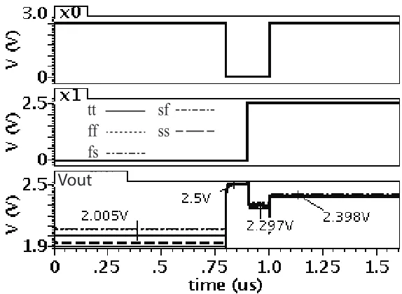
is performed, and the result of that is shown in Fig. 2.6 as well to investigate the process
variation effect on the output result. The maximum output fluctuation of the voltage DAC
happens forx1x0 = 01 whereVS changes from1.93V at f f to 2.07V at f s conditions.
In this case, VS is supposed to be equal to 2V and is correspondent to the hard-limit
neuron shape and does not affect the neuron shape significantly. Moreover, the hard
-limitneuron shape is considered the coarse tuning when used in multiresolution learning paradigm [5]; meaning that small variations in the transfer function can be compensated
during the fine-tuning stages. The dimensions of transistorsM14−18are 0.225, 1.225, 1.225, 42.2,
and 32.8 respectively.
The process and temperature variations impact on the neuron function is investigated
by performing the corner analysis for the neuron transfer function. The post-layout
sim-ulations are shown in Fig. 3.6 for a = 0.1, a = 1.2 at VG = 800mV and for the linear
function atVG = 200mV and at the temperatures of 27C, -55C, and 125C. The deviation
from thett(Typical NMOS Typical PMOS) condition at the room temperature of 27C is represented in Fig. 2.8. As shown in this figure, the maximum deviation occurs at thef f
2. RECONFIGURABLE NEURON PWL APPROXIMATION BASED ON THE MINIMUM OPERATOR
Er
ror
125,
ff
-55,
ff
-55,
sf
Figure 2.8: The corner and temperature post-layout analysis for different conditions off f,
ss, sf, and f s at temperatures of 27C, -55C, and 125C showing the deviation from the activation function at 27C.
Similar to other analog structures, the proposed neuron is disposed to mismatch.
How-ever, the parametric analysis simulation results show that the circuit works well by
con-sidering 10% mismatch of transistors. It should be noted that the proposed neuron when used in an on-chip or a chip-in-the-loop configuration, can enjoy some flexibility because
the adaptation of the synapses during the training will be based on the actual and physical
characteristics of the fabricated neuron. Moreover, the mechanism for adjusting the neuron
transfer function allows more flexibility in the transistor mismatches while the network is
getting trained.
2.5
Conclusion
A novel reconfigurable neuron is proposed in this paper to be used in analog and
mixed-signal neural networks with different requirements. The shape of the neuron can be changed
2. RECONFIGURABLE NEURON PWL APPROXIMATION BASED ON THE MINIMUM OPERATOR
function and the controllability is obtainable by adjusting the substrate voltage of PMOS
transistors. A 2-bit voltage DAC is used to adjust the shape of the neuron on or off-chip.
The proposed structure is an invaluable part of the analog or mixed-signal networks that
References
[1] C. H. sai, Y. T. Chih, W. H. Wong, and C. Y. Lee, “A Hardware-Efficient Sigmoid Func-tion With Adjustable Precision for a Neural Network System,” IEEE Trans. Circuits Syst. II, vol. 62, no. 11 pp. 1073–1077, Nov. 2015.
[2] Q. Liu, and J. Wang, “Finite-Time Convergent Recurrent Neural Network with a Hard-Limiting Activation Function for Constrained Optimization with Piecewise-Linear Ob-jective Functions,”IEEE Trans. Neural Netw., vol.22, no.4, pp. 601–613, Mar. 2001.
[3] T. Qiu, X. Wen, and F. Zhao, “Adaptive-Linear-Neuron-Based Dead-Time Effects Compensation Scheme for PMSM Drives,”IEEE Trans. Power Electron., vol. 31, no.3, pp. 2530–2538, Mar. 2016.
[4] Yang Zhang, Yi Li, Xiaoping Wang, and Eby G. Friedman, “Synaptic Characteristics of Ag/AgInSbTe/Ta-Based Memristor for Pattern Recognition Applications,IEEE Trans. Electron. Dev., vol. 64, no. 4, pp. 1806-1811, Apr. 2017.
[5] Y. Liang and X. Liang, “Improving signal prediction performance of neural networks through multiresolution learning approach,” IEEE Trans. Syst., Man, Cybern. B, vol. 36, no. 2, pp. 341–352, Apr. 2006.
[6] G. Khodabandehloo, M. Mirhassani, and M. Ahmadi, “A Prototype CVNS Distributed Neural Network Using Synapse-Neuron Modules,”IEEE Transactions on Circuits and Systems I: Regular Papers, vol. 59, no. 7, pp. 1482–1490, 2012.
[7] D. Moro-Frias,C. A. De La Cruz-Blas, and M. T. Sanz-Pascual,“PWL Current-Mode CMOS Exponential Circuit Based on Maximum Operator,” IEEE Antennas Wireless Propag. Lett., vol.5, no.1, pp. 450-453, Dec. 2006.
[8] H. B. Demuth, M. H. Beale, O. De Jess,M. T. Hagan,Neural network design, 1996.
REFERENCES
Chapter 3
Mixed-Signal Synapse Multipliers for
Feed-Forward Neural Networks
3.1
Introduction
In Analog Neural Networks (Analog NN) [1, 2, 3] neurons can be realizing with simple and
elegant non-linear analog circuits and with only a few transistors. Moreover, the addition
of values can be performed by simple nodal summation of currents as long as it can drive
the circuit of the next stage. However, the accuracy of analog circuits has always been a
limiting factor for the realization of large size multi-layer Analog NNs. A multi-layer
net-work requires storing a large number of synaptic values. In analog circuits, these values are
typically stored on capacitors which may change due to leakage currents; hence, periodic
refreshments are required. The issue of storage has been proven to cause limitation in size
and complexity of such networks.
imple-3. MIXED-SIGNAL SYNAPSE MULTIPLIERS FOR FEED-FORWARD NEURAL NETWORKS
mentations [4, 5, 6, 7]. In such systems, advantages of both analog and digital [9, 10, 11, 8]
domains are gathered in one place in order to overcome the design challenges to accomplish
smaller area, lower power consumption, higher speed, and smoother activation function
re-alization.
One of the most efficient approaches to implement the synapse in mixed-signal circuitry
is based on the Multiplying Analog to Digital Converter (MDAC) which is used to multiply
the synapse value by the neuron input. Conventional MDACs work based on the weighted
summation of currents, that means weighted current mirrors are required in the network.
Therefore, in each layer of the network with N neurons, N2 MDAC units are required.
Optimization of the size of the multiplier would significantly affect the feasible size of the
network and hence its performance.
In this chapter, a programmable mixed-signal MDAC multiplier is proposed to be used
in the feed-forward neural network. The proposed structure is modular and easy to be
adopted for different network configurations while the area is reduced by using digital gates
to ease the multiplication and avoid using large-size transistors. Moreover, synaptic weights
are stored in registers which eliminate the need for capacitors and refreshing circuitries.
3.2
Neural Network Configurations
In this section, the general configuration of one layer of the mixed-signal neural network
is presented. There are three main building blocks for the mixed-signal implementation of
neural networks: programmable MDACs for synapse multipliers, adders, and non-linear
neurons that create an integrated synapse-neuron building block.
In the proposed architecture, multiplication operation between the synaptic weights and
the network inputs is performed by the MDAC, where synaptic weights are stored in digital
registers and are multiplied by the analog inputs. Multiplication result of each multiplier
3. MIXED-SIGNAL SYNAPSE MULTIPLIERS FOR FEED-FORWARD NEURAL NETWORKS
Figure 3.1: System-level configuration of the proposed mixed-signal neural network.
from other blocks.
Fig. 3.1 shows the block diagram of a sample 2-2-1 network. As it can be seen in this
figure outputs of n building blocks are connected in parallel to generate a neuron. The number of MDACs in each layer is equal to the number of inputs to that layer.
The digital registers store the value of the synaptic weight and are programmable based
on the network training. The weights are denoted by Ymn in this figure, where m and n
represent the number of corresponding neuron and inputs of each layer, respectively.
Since the circuit design is based on the current-mode operation, addition in the network
is based on the summation of currents. Neurons are resistive non-linear functions which
are distributed in the network.
The proposed network is trained off-line, where weights and network parameters are
calculated off the chip and downloaded later into the weight registers. However, the
net-work can be easily adjusted for on-line training by adding extra hardware for weight
3. MIXED-SIGNAL SYNAPSE MULTIPLIERS FOR FEED-FORWARD NEURAL NETWORKS
I
inBias2
Bias1
V
outM
1M
4M
3M
2Figure 3.2: General configuration of the mixed-signal neural network[7].
3.3
Building block’s components
Neuron and its simulation result are presented in this section, followed by the proposed
multiplier structure that plays an important role in reliability and accuracy of the network.
3.3.1
Neuron
Neurons for this network are resistive-type and distributed in order to increase the signal
to noise ratio of the network [7, 5]. The neuron transfer function self-adjusts, preventing
the saturation of neurons when the total number of input increases. The neuron uses the
fundamental nonlinearity in V-I characteristics of the MOS transistors to approximate the
sigmoid-like function. Fig. 3.2 represents the resistive-type neuron. The 6-transistor design
[7] is biased to operate in both triode and saturation regions and has an accurate
approxi-mation to the original sigmoid function. The simulation result of the transfer function of
3. MIXED-SIGNAL SYNAPSE MULTIPLIERS FOR FEED-FORWARD NEURAL NETWORKS
Figure 3.3: Non-linear neuron activation function which approximates the sigmoid func-tion.
y
0x
0x
1x
2x
3y
1y
2y
3y
0y
1y
2y
3y
0y
1y
2y
3y
0y
1y
2y
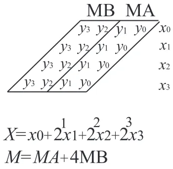
3X=x
0
+
2
x
1+
2
x
2+
2
x
3
M=MA
+
4MB
2
1
3
MA
MB
Figure 3.4: Multiplying the two less significant and the two most significant bits of Y with the analog value of the input X
3.3.2
Mixed-Signal Multiplier
In its most general form, multiplication between two binary values (X, and Y) can be
3. MIXED-SIGNAL SYNAPSE MULTIPLIERS FOR FEED-FORWARD NEURAL NETWORKS
y1
y0 S 0A
y1
y0 S 2A
y1
y0 S 1A
y3
y2 S 0B
y3
y2 S 2B
y3
y2 S 1B
Wp/Lp Wp/Lp
S2A
S0A
1 3 2
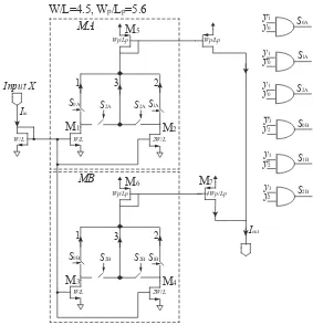
S1A S2A Input X MA 4Wp/Lp W/L W/L 2W/L Iin Iout
W/L=4.5, Wp/Lp=5.6
M1 M5 M7 M2 Wp/Lp S2B S0B
1 3 2
S1B S2B MB W/L 2W/L M3 M6 M4
Figure 3.5: The proposed modular mixed-signal multiplier to be used in distributed feed-forward neural network
wherexi andyj areithandjthbit of X and Y respectively. In mixed-signal multiplication,
one of the numbers (X) is an analog value. the synapse receives an analog input and
mul-tiplies it by a digital weight in the first layer. The multiplication result passes the S-shaped
nonlinear neuron; then it is added to other multiplication results come from other branches
in the first layer.
In conventional MDACs, the principle of multiplying is to use weighted current mirrors.
That means that if the size of the first transistor in a weighted current mirror is W/L, we
need transistors of the size of twice, four times, and eight times of W/L are required to
per-form the digital to analog multiplication and conversion. The proposed modular multiplier
multi-3. MIXED-SIGNAL SYNAPSE MULTIPLIERS FOR FEED-FORWARD NEURAL NETWORKS
plication. In the proposed approach, the analog input is multiplied to two bits of the digital
weight (Y). Fig. 3.4 represents the concept of multiplication of two least and most
signif-icant bits of the weight (Y) to the analog input of X separately. Based on this separation,
the multiplication result from (1) can be rewritten as:
M A= (y0+ 2y1)·(x0+ 2x1+ 22x2+ 23x3) (3.2)
M B = (y2+ 2y3)·(x0+ 2x1+ 22x2+ 23x3) (3.3)
As it can be seen in equation (2), the output of the MA block can be 0, X, 2X, or 3X
depending on what the value of y0 andy1 are. In this method, combinations ofy0 andy1
are used to generate controlling signals that let 0, X,2X or the addition of them (3X) pass
through to the output. The MB block has the same structure as the MA but it’s controlling
signals are generated by combinations ofy2 andy3.
Fig. 3.5 represents the modular architecture for a 4-bit to 4-bit equivalent mixed-signal
multiplier. In this figure,SiAandSjB are controlling signals generated by pair ofy0andy1
and pair ofy2 andy3. Respectively. S0A(S0B) lets the same value of input X pass through
M1 (M3) ify1y0 (y3y2)=01. Due to the same logic, twice of the value of X passes through
M2(M4) when y1y0 (y3y2)=10. When y1y0 (y3y2)=11, passes 1 and 2 are open and the
addition of M1 (M3) and M2(M4) passes through M5 (M6) which is output of MA (MB)
block.
To confirm the validity and accuracy of the operation, the simulation result and ideal
expected multiplication result for Y=1111 are compared in Table I. In case of Y=1111,
MA and MB reach their maximum values that fully load the multiplier. In this case, the
error and power consumption are at their maximum levels. Also, they have the same value
because of the modularity of the design. As it can be seen in this table the maximum error
3. MIXED-SIGNAL SYNAPSE MULTIPLIERS FOR FEED-FORWARD NEURAL NETWORKS
0 5 10 15
0 10 20 30 40 50
Input current (X)
Multiplication result (MA/MB)
tt ff ss sf fs
Figure 3.6: MA/MB output result for Y=1111for corner analysis fast-fast (ff), slow-slow (SS), slow-fast (sf) and fast-slow (fs) to show the process variation effect.
0 1 2 3 4 5 6 7 8 9 10 11 12 13 14 15
0 50 100 150
Input Current (X)
Multiplication Resul
t y=1011
y=1100
y=0111 y=0010
y=1010
Figure 3.7: Multiplication results for Y=0010, 0111, 1010, 1011, and 1100. Ideal and simulation results are shown with dashed and solid lines respectively.
percentage is 1.3% for 4µA. Corner analysis results represented in Fig. 3.6 shows the result considering process variations.
The multiplication results for more five digital weights and the ideal multiplication
results for an input range of 0 to 15µA is shown Fig. 4.6. The maximum error of 0.24µA which is one-fourth of the multiplier accuracy of 1µA. That means the error is not only within the acceptable range but also it can increase the accuracy to 5 bit.
To confirm the validity and accuracy of the operation, the simulation result and ideal


![Figure 3.2: General configuration of the mixed-signal neural network[7].](https://thumb-us.123doks.com/thumbv2/123dok_us/1363574.1169163/50.612.230.419.103.266/figure-general-conguration-mixed-signal-neural-network.webp)
![Figure 4.5: The modular signed multiplying DAC that performs as the synapse [12]. Tis connected to the terminal with the same name in Fig](https://thumb-us.123doks.com/thumbv2/123dok_us/1363574.1169163/66.612.179.470.109.396/figure-modular-signed-multiplying-performs-synapse-connected-terminal.webp)

