Study the Development and Operation of
Discrete Vertical Drain Lateral-Diffused MOS
(VDMOS) Power Transistors
Deepika Sharma1, Bal krishan2
Student, Dept. of Electronics Engineering, YMCA University of Science and Technology, Faridabad, India Assistant Professor, Dept. of Electronics Engineering, YMCA University of Science and Technology, Faridabad,
India
ABSTRACT: Due to scaling limitations, a conventional MOSFET cannot be used in high power applications. So for increasing RF application demand, a MOSFET was created known as VDMOSFET. This paper gives a brief review of VDMOSFET’s construction and its working. Various parameters affecting its operation have also been discussed.
KEYWORDS: VDMOS, Threshold voltage, Gate oxide thickness, Threshold implantation, Channel doping
I. INTRODUCTION
A conventional lateral MOSFET structure cannot be easily scaled for high power applications due to two main reasons. First, a large spacing between drain and source is required to achieve a high voltage blocking capability. To get this, channel length must exceed the thickness of the space charge (SC) region on the channel side of the drain junction to avoid punch through. This results in wastage of larger surface area of the semiconductor using a lateral structure to reinforce the high drain voltage and to avoid punch through. Also having a longer channel will increase channel resistance and reduce the current rating of the device. Second, in the lateral MOSFET structure metallisation becomes complicated because all the connections i.e. source, drain and gate are created on the same upper surface. Both effects consume more area, resulting in a low silicon utilization factor. Due to these reasons, the simple lateral MOSFET structures are seldom used as power distinct devices. Conventional mosfets cannot be used for power applications by simply decreasing channel length of the device. Fig1 shows the diagram of conventional lateral mosfet.
Fig.1 The cross-sectional view of a conventional MOS transistor
II. DEVELOPMENTOFPOWERMOSDEVICES
groove in the semiconductor surface after the p-body region and n+ diffusion an anisotropic etch was used. By connecting many individual devices in parallel during the metallization process a large current rating can be achieved. From the two sources (each sides of the groove) each gate of the vmosfet controls the current. Fig 2 shows the structure of vmosfet.
Fig. 2. Cross-sectional view of a VMOSFET [6]
As the current is overfilling at the spike of gate, it can decrease the useful current rating of the device as well as the voltage rating. This problem can be lowered by using the truncated vmosfet. Fig 3 shows the structure of truncated vmosfet.
Fig. 3. The cross-sectional view of a truncated VMOSFET[7]
To expound two closely placed pn junctions at different depths below the silicon surface a vmosfet utilizes two successive diffusion steps. This dual diffusion technique can be used laterally in the same manner. The device structure called LDMOS. In this structure the channel length does not depend on the lithography step as in conventional lateral mosfets; rather it depends on the diffusion processes. Fig 4 shows the cross sectional view of LDMOS.
The power mosfet design incorporates the proposal of VMOSFET and LDMOS. This structure is known as the vertical-diffused mosfet. The vdmos structure exploits the dual diffusion technique to determine the lateral surface channel length as in LDMOS and supports the drain voltage vertically in the n- epilayer as in VMOSFET. The electrons first flow laterally from the source through the channel and then flow vertically down through the n- epilayer to the substrate drain contact. Fig 5 shows the complete structure of vdmosfet.
Fig. 5. The cross-sectional view of a VDMOS [7]
III.DEVICECHARACTERISTICS:STATICOPERATION
VDMOS characteristics are much like those of conventional mosfets. It has four distinct operation regions formed between the source (formed by n+ diffused region) and the substrate (n+ drain region) when it is working in active mode. Region A is the surface layer of the body region. At a given gate voltage the channel will form at this region. Region B is the surface layer of the body region between the source diffusions. Region C is the regions between body regions. Region D is the drain drift region in the epilayer. Any blocking voltages are developed across the region D whereas region A controls the flow of current in the device [7]. Fig 6 is showing all active regions of vdmos.
Fig. 6. The cross sectional view of a VDMOS showing the active region.[7]
A. Threshold Voltage:
change in VT. So, it is important to grow the gate oxide layer under extremely clean condition. Threshold voltage has negative temperature coefficient. Fig 7 is showing the variation in VT in accordance with NA and Qox at room temperature.
Fig. 7. The effect of NA and Qox on VT at room temperature
B. On Resistance
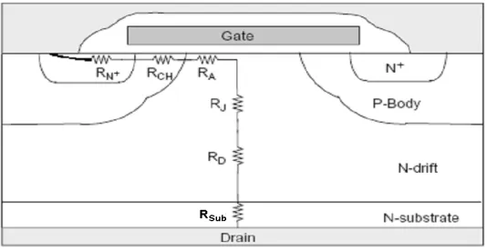
The total on state resistance (RDS(on)) of a vdmos is defined as the sum of various different resistances i.e. the resistance of the inverted channel (RCH), the spreading resistance of the accumulation region formed in the surface of the epilayer (RA), the resistance of the bulk semiconductor – the drain region (RD0), and the resistance of the substrate (RSub).
RDS(on) = RCH + RA + RD0 + RSUB eq. (1)
where RD and RJ, affects the on state resistance more at high voltages because higher resistivity (low doped) and thickness values in the epilayer are required for higher voltage devices. RSUB can be ignored at higher voltages. RCH affects more RDS at lower voltages. At lower value of RDS(on), on-state power loss is minimum and current rating is maximum of the device. It results with superior power-switching performance since the voltage drop from drain to source is also minimized for a given value of drain-to-source current [4]. RDS(on) is dependent on the temperature as the mobility of holes and electrons decreases as temperature increases
Fig. 8. A VDMOS transistor showing its internal resistances (RDS(on))[6]
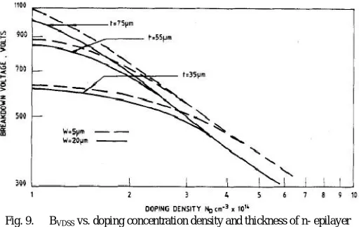
Breakdown voltage (BVDSS) is the maximum voltage between drain to source that a MOS transistor can hold without causing avalanche breakdown of the pn junction formed at the body-drain region in the off-state. There are five important elements that controls breakdown i.e. avalanche, reach-through, punch-through, Zener and dielectric breakdown [6].
Voltage blocking in vdmos is structured between the p- body region and the n- epilayer region (region C and D in Fig. 6). In the case of an n-channel, enhancement mode vdmos, almost all the blocking voltage (breakdown voltage limit) is supported by n-epilayer that is why BVDSS depends doping profile and thickness of n-epilayer. To produce a higher breakdown voltage, both the resistivity and the thickness of the n- epilayer need to be increased [12]. Fig.9 shows the effect of doping concentration and thickness for the n- epilayer on the BVDSS.
Fig. 9. BVDSS vs. doping concentration density and thickness of n- epilayer
Breakdown voltage also depends on the shape of the junction and the structure of the region where the junction encounter the semiconductor surface. This is due to the change in electric field at the edge of junctions. As the electric field is increased, the breakdown voltage of a device decreases.
IV.CAPACITIVEELEMENTS&DYNAMICBEHAVIOR
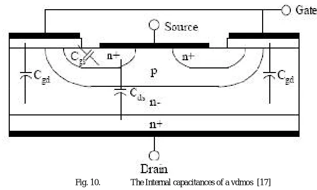
The high frequency interpretation of a vdmos is decided by the time required to create voltage changes across capacitances. That is why having knowledge about the internal capacitance of a vdmos is important. The capacitances incorporate CGS (the capacitance between gate electrodes to the source region; independent of applied voltage), CDS(the capacitance between the n+ drain to source region; inversely proportional to the square root of VDS), and CGD (the capacitance between the gate electrodes to the n+ drain region is a nonlinear function of voltage due to variation in n- depletion). Three capacitances mostly used are the input capacitance (CISS), the output capacitance (COSS), and the reverse transfer (or Miller) capacitance (CRSS). CISS is the parallel combination of CGD and CGS. COSS is the parallel combination of CDS and CGD. CRSS is same as CGD.
Fig. 10. The Internal capacitances of a vdmos [17]
The maximum operating frequency of power MOS transistors can be found using equation
f
max≤
( )eq. (3)
where ton is the overall turn-on time and toff is the overall turn-off time [1]. Before the device begins to turn on, CISS must be charged to the threshold voltage and discharged to the certain voltage before the device turns off. For this reason, CISS has a direct effect on the turn-on and turn-off time of the device. If CGS and CGD can be reduced, it is possible to work in the high frequency regime. Fmax is directly proportional to GFS and inversely proportional to CISS. Fig 10 shows the internal capacitance of vdmos.
V.VDMOSPARASITICBJT
A vdmos has a parasitic BJT as an internal element of its structure. The n+ source terminal correlates with the n-type emitter, the p- body region correlates with the p-n-type base, and the n-n-type drain correlates with to the n-n-type collector. Vdmos will completely short –circuit if the parasitic BJT turns on. So it must be made certain that the parasitic device is in cut-off mode at all times. By shorting the source (emitter) and body (base) regions, parasitic device conquers in static mode of operation resulting in stopping the device from ever creating an emitter-base voltage [7]. However, the parasitic BJT can commence during the high-speed switching operation of the vdmos. The rate of the rise of the VDS can be very high in the inductive load circuits.
Fig. 11. The cross-section of a VDMOS showing a parasitic BJT
VI. CONCLUSION
The parasitic BJT effect in vdmos can be reduced by implanting higher doping diffusion in p-region which reduces the RBB value. This extra implantation has no effect on the other characteristics of the device. This extra implant is known as UIS (unclamped inductive switching) implant. It is used to verify the vdmos operation and resistance against this parasitic effect.
REFERENCES
1. V. Benda, J. Gower , and D. A. Grant, Power Semiconductor Devices: Theory and Applications, Chichester: John Wiley & Sons, Inc, 1999. 2. K. S. Oh, “IGBT Basics 1: Application Note 9016,” Fairchild Semiconductor, February 2001.
3. V. Barkhordarian. “Power MOSFET Basics: AN1084,” International Rectifier, July 2000.
4. “Understanding Power MOSFETs: Application Note An-7500,” Fairchild Semiconductor, October1999. 5. C. G. Jambotkar. “Power Field Effect Transistor.” U.S. Patent 4,145,700, March20, 1979.
6. K. S. Oh, “MOSFET Basics: AN9010” Fairchild Semiconductor, July 2000.
7. D. A. Grant and J. Gowar, Power MOSFET: Theory and Applications, New York: John Wiley & Sons, Inc, 1989.
8. Y. Tarui, Y. Hayashi, and T. Sekigawa, “Diffusion self-aligned MOST: A new approach for high speed devices.” Proc. Conf. Solid State Devices 1, 105 110,1969.
9. P. H. Wilson. “A Novel High Voltage RF Vertical MOSFET for High Power Applications,” IEEE, pg 95-100, 2002. 10. M. Trivedi and K. Shenai. “Comparison of RF Performance of Vertical and Lateral DMOSFET,” IEEE, pg 245-8, 1999. 11. “The RF MOSFET Line. RF Power Field-Effect Transistor: N-Channel Enhancement-Mode,” Tyco Electronics. 12. “Power Semiconductor Applications,” Philips Semiconductors, pg 21.
13. D. A. Neamen. Semiconductor Physics and Devices. Boston: McGraw-Hill, 2003.
14. M. N. Darwish and K. Board. “Optimization of Breakdown Voltage and On- Resistance of VDMOS Transistors,” IEEE Transactions on Electron Devices, Vol. ED-31, No. 12, pg 1769-1775, 1984.
15. J. Dodge. “Power MOSFET Tutorial,” Application Note: APT-0403, pg. 1-12, March 2006.
16. S. K. Leong. “Obtaining DMOS Power RF Transistor Information from Published Data Sheets.” RF featured technology, pg. 26-32, 1993. 17. A. Grimaldi, A. Schiliaci, A. Vitanza, and E. Romano. “Ruggedness Improvement of RF DMOS Devices: AN1232,” July 2000. 18. F. Frisina. “Fabrication of VDMOS Structure with Reduced Parasitic Effects,” U.S. Patent 6,391,723, May 21, 2002.
19. L. A. Goodman and A. M. Goodman. “Method for Making Vertical MOSFET with Reduced Bipolar Effects,” U.S. Patent 4587,713, May 13, 1986. 20. C. Contiero, A. Andreini, and M. Galbiati. “Self-Aligned Process for Fabricating small DMOS Cells,” U.S. Patent 4,774,198, Sep. 27, 1988. 21. J. D. Plummer, M. D. Deal, and P. B. Griffin. Silicon VLSI Technology .Fundamentals, Practice and Modeling. New Jersey: Prentice Hall, 2000.
BIOGRAPHY
Deepika Sharma is a M.Tech.Student (VLSI Design) in Electronics Engineering Department, YMCA University of Science and Technology, Faridabad. Her research interests are fabrication and simulation of nanoscale devices.
![Fig. 2. Cross-sectional view of a VMOSFET [6]](https://thumb-us.123doks.com/thumbv2/123dok_us/1452379.1177928/2.595.192.409.626.757/fig-cross-sectional-view-vmosfet.webp)
![Fig. 5. The cross-sectional view of a VDMOS [7]](https://thumb-us.123doks.com/thumbv2/123dok_us/1452379.1177928/3.595.169.429.545.696/fig-cross-sectional-view-vdmos.webp)