Electronic Theses and Dissertations Theses, Dissertations, and Major Papers
2011
Arithmetic with the Two-Dimensional Logarithmic Number
Arithmetic with the Two-Dimensional Logarithmic Number
System (2DLNS)
System (2DLNS)
Mahzad Azarmehr University of Windsor
Follow this and additional works at: https://scholar.uwindsor.ca/etd
Recommended Citation Recommended Citation
Azarmehr, Mahzad, "Arithmetic with the Two-Dimensional Logarithmic Number System (2DLNS)" (2011). Electronic Theses and Dissertations. 430.
https://scholar.uwindsor.ca/etd/430
by
Mahzad Azarmehr
A Dissertation
Submitted to the Faculty of Graduate Studies through
the Department of Electrical and Computer Engineering in Partial Fulfillment
of the Requirements for the Degree of Doctor of Philosophy at the
University of Windsor
Mahzad Azarmehr
APPROVED BY:
D. Al-Khalili
Department of Electrical and Computer Engineering, Royal Military College
A. Edrisy
Department of Mechanical, Automotive and Materials Engineering, University of Windsor
R. Muscedere
Department of Electrical and Computer Engineering, University of Windsor
M. Khalid
Department of Electrical and Computer Engineering, University of Windsor
M. Ahmadi
Department of Electrical and Computer Engineering, University of Windsor
A. T. Alpas
Department of Mechanical, Automotive and Materials Engineering, University of Windsor
This thesis includes 2 original papers that have been previously published/submitted for
publication in peer reviewed journals, as follows:
Thesis Chapter Publication title Publication status
Chapters 4 and 5 High-Speed and Low-Power Reconfigurable Architecture of 2-digit 2DLNS-based Recursive Multipliers Published Chapter 6 Low-Power Finite Impulse Response (FIR) Filter Design using Two-Dimension Logarithmic Number System (2DLNS) Representations Submitted
There are several people who deserve to be acknowledged for their generous contributions to this project. I would first like to express my sincere gratitude and appreciation to Dr. Majid Ahmadi, my supervisor, for his invaluable guidance throughout the course of this thesis work. I would also like to thank my committee members: Dr. Afsaneh Edrisy, Dr. Roberto Muscedere, Dr. Mohammed Khalid, and Dr. Dhamin Al-Khalili from the Royal Military College for reviewing my thesis and their constructive comments. Special thanks to Dr. Roberto Muscedere for his expert guidance and constant support throughout my study.
Declaration of Previous Publication iv
Abstract vi
Dedication viii
Acknowledgments ix
List of Figures xiv
List of Tables xvi
List of Abbreviations xvii
1 Introduction 1
1.1 Introduction . . . 1 1.2 Thesis Objectives . . . 5 1.3 Thesis Organization . . . 5
2 The Multi-Dimensional Logarithmic Number System 7
2.4 Conversion . . . 12
3 2DLNS Arithmetic 14 3.1 2DLNS Addition/Subtraction . . . 14
3.2 2DLNS Multiplication . . . 19
3.2.1 2DLNS Multiplier with Binary Addition . . . 20
3.2.2 2DLNS Multiplier with 2DLNS Addition . . . 20
3.2.3 Synthesis Results and Comparison . . . 21
3.2.3.1 8-bit by 8-bit Multiplier . . . 22
3.2.3.2 16-bit by 16-bit Multiplier . . . 22
3.2.3.3 32-bit by 32-bit Multiplier . . . 23
3.2.3.4 Conclusions . . . 24
4 2DLNS Recursive Multiplication 25 4.1 Overview of the Recursive Multiplication Algorithm . . . 25
4.2 One-level Recursion . . . 26
4.3 Two-level Recursion . . . 29
4.4 Synthesis Results and Comparison . . . 30
4.5 Conclusions . . . 33
5 Reconfigurable Multiplier Architectures 35 5.1 Reconfigurable Architectures . . . 36
5.2 Reconfigurable 2DLNS-based Multipliers . . . 36
5.3 Synthesis Results and Comparison . . . 44
5.4 Conclusions . . . 46
6 Finite Impulse Response (FIR) Filter Design 47 6.1 FIR Filter Architecture . . . 48
6.2.1 Binary-based Design . . . 50
6.2.2 2DLNS-based Design . . . 52
6.2.3 Recursive 2DLNS-based Design . . . 56
6.2.4 Synthesis Results and Comparison . . . 59
6.3 32-bit Input Signal . . . 61
6.3.1 Binary-based Design . . . 62
6.3.2 2DLNS-based Design . . . 63
6.3.3 Recursive 2DLNS-based Design . . . 63
6.3.4 Synthesis Results and Comparison . . . 65
6.4 Conclusions . . . 66
7 Conclusions and Future Works 68 7.1 Conclusions . . . 68
7.2 Suggestions for Future Works . . . 69
References 71 A Hardware Description Codes 75 A.1 Packages . . . 75
A.2 The Filter Modules . . . 83
A.2.1 TheFilter. . . 84
A.2.2 The Input Register . . . 88
A.2.3 The Binary / 2DLNS Converter . . . 89
A.2.4 The Binary / 2DLNS Conversion Register . . . 121
A.2.5 The Multiply and Accumulate unit (MAC) . . . 122
A.2.5.1 The Exclusive-or unit . . . 129
A.2.5.2 The First Exponent Adders . . . 130
A.2.5.3 The Second Exponent Adders . . . 131
A.2.5.5 24-bit Adder / Subtractor . . . 139
A.2.5.6 25-bit Adder / Subtractor . . . 140
A.2.5.7 18-bit Adder / Subtractor . . . 141
A.2.5.8 34-bit Adder / Subtractor . . . 142
A.2.5.9 50-bit Adder / Subtractor . . . 144
A.2.5.10 Accumulator Register . . . 145
A.2.6 The Controller . . . 145
A.3 The Filter Test . . . 151
A.3.1 TheFilterTest Bench . . . 151
A.3.2 The Test Bench Clock Generator . . . 154
A.3.3 The Test Bench Coefficient Memory . . . 155
A.3.4 The Test Bench Data Memory . . . 157
A.3.5 The Test Bench Input Data Reader . . . 161
3.1 The 1-digit 2DLNS Adder . . . 17
3.2 The 1-digit 2DLNS Subtractor . . . 18
3.3 The 1-digit 2DLNS Multiplier . . . 19
3.4 The 2-digit 2DLNS Multiplier with Binary Adders . . . 20
3.5 The 2-digit 2DLNS Multiplier with 2DLNS Adders . . . 21
4.1 One-Level Recursive Multiplier . . . 27
4.2 The 2-digit 2DLNS-based Recursive Multiplier (One-Level Recursion) . . . 28
4.3 Two-Level Recursive Multiplier . . . 30
4.4 The 2-digit 2DLNS-based Recursive Multiplier (Two-Level Recursion) . . 31
5.1 The Reconfigurable 2-digit 2DLNS based Recursive Multiplier (One-Level Recursion) . . . 37
5.2 The Reconfigurable 2-digit 2DLNS based Recursive Multiplier (Two-Level Recursion) . . . 38
5.3 Double Precision Multiplier (One-Level Recursion) . . . 40
5.4 Double Precision Multiplier (Two-Level Recursion) . . . 40
5.5 Single Precision Multiplier (One-Level Recursion) . . . 41
5.6 Single Precision Multiplier (Two-Level Recursion) . . . 41
5.7 Dual Single Precision Multiplier (One-Level Recursion) . . . 42
5.9 Single Precision Fault Tolerant Multiplier (One-Level Recursion) . . . 43
5.10 Single Precision Fault Tolerant Multiplier (Two-Level Recursion) . . . 43
6.1 The Systolic Structure for a FIR Filter . . . 48
6.2 The Magnitude Response of a Band Pass Filter . . . 49
6.3 The Filter Input Signal . . . 50
6.4 The Binary Filter Output Signal . . . 52
6.5 The Filter and Auxiliary Modules . . . 53
6.6 The Filter RTL Components . . . 54
6.7 The MAC Unit Structure . . . 55
6.8 The 2DLNS Filter Output Signal . . . 56
6.9 The MAC Unit Structure in Recursive Architecture . . . 57
6.10 The Recursive 2DLNS Filter (Split Coefficients) Output Signal . . . 58
6.11 The Recursive 2DLNS Filter (Genuine Coefficients) Output Signal . . . 59
6.12 The Filter Input Signal . . . 61
6.13 The Binary Filter Output Signal . . . 62
6.14 The 2DLNS Filter Output Signal . . . 63
6.15 The Recursive 2DLNS Filter (Split Coefficients) Output Signal . . . 64
3.1 8×8bit Multiplier Synthesis Results . . . 22
3.2 16×16bit Multiplier Synthesis Results . . . 23
3.3 32×32bit Multiplier Synthesis Results . . . 23
4.1 64×64bit Recursive Multipliers Synthesis Results . . . 32
5.1 Reconfigurable Recursive Multipliers Synthesis Results . . . 44
6.1 16-bit Binary-based Designs Synthesis Results . . . 51
6.2 2DLNS-based Designs Synthesis Results . . . 56
6.3 16-bit FIR Filter Designs Synthesis Results . . . 60
6.4 32-bit Binary-based Designs Synthesis Results . . . 62
ADC Analog to Digital Converter ALU Arithmetic and Logical Unit
ASIC Application Specific Integrated Circuit
BIBO Bounded Input-Bounded Output
CMOS Complementary Metal-Oxide-Semiconductor
DFT Discrete Fourier Transform DSP Digital Signal Processing
FIR Finite Impulse Response
I/O Input/Output
IEEE Institute of Electrical and Electronics Engineers IIR Infinite Impulse Response (IIR)
LNS Logarithmic Number System
LUT Look Up Table
MAC Multiply and Accumulate
MDLNS Multi-Dimensional Logarithmic Number System RALUT Range Addressable Look Up Table
RAM Random Access Memory
ROM Read Only Memory
RTL Register Transfer Level
SBD Single Base Domain
TSMC Taiwan Semiconductor Manufacturing Company.
VHDL VHSIC Hardware Description Language
VHSIC Very High Speed Integrated Circuit VLSI Very Large Scale Integration
Introduction
1.1
Introduction
In most real-time Digital Signal Processing (DSP) applications, high performance is a prime target. Here, performance may be interpreted as a combination of speed, power consumption, precision, and VLSI area efficiency.
The dynamic range of the data usually used in DSP may be best suited to floating-point representations, but the dynamic range of floating-point comes to the cost of lower preci-sion and increased complexity.
cost of complicated and inexact addition and subtraction, as well as the need to convert between binary and logarithmic formats [3].
Using Analog to Digital Converters (ADC), that benefit from the exponential current-voltage characteristics of bipolar transistors or MOS transistors operating in weak inver-sion, provides a natural logarithmic input to an LNS system.
In this regard, two techniques were presented in [8]; linear approximation by using different-sized approximation intervals and non-linear compression, which reduces table spaces by sorting the difference between the exact value of the function and a linear approximation across smaller regions where the function is more non-linear. In [9], the error caused by interpolation is simultaneously evaluated and accumulated into the result; thereby the error is corrected with a delay of one extra carry save adder stage.
Coleman et al. were the first research group to start with the design and implementation of an LNS Arithmetic and Logical Unit (ALU) [9]. They examined some practical DSP appli-cations and then applied it to an LNS Microprocessor [10]. The essence of their work was to develop an efficient algorithm for logarithmic addition and subtraction. It has been claimed that their European Logarithmic Microprocessor (ELM), as the first microprocessor de-vice to use the LNS instead of floating-point for real arithmetic, delivers approximately two fold improvements in speed and accuracy [11]. The main idea in ELM is that given an LNS addition and subtraction procedure capable of operating with speed and accuracy at least equivalent to that of floating-point, the system can offer an overall advantage for arithmetic operations [12].
Another LNS ALU design has been presented in [13]. This design takes benefit from an interpolator that accepts both positive and negative arguments with a new addition scheme which reduces the critical path and provides a shorter latency. The three methods of in-terpolation, multipartite tables and co-transformation for LNS addition and subtraction have been compared in [14]. In this research work, a library for a novel version of co-transformation was also proposed that provides more accurate results at the cost of an increase in the latency of the hardware.
the latter design is superior.
Considering all the above, it can be concluded that LNS architectures are perfectly suited for low-power and low-precision DSP problems. The major drawback of LNS are the needs to implementing efficient techniques for data conversion and logarithmic addi-tion and subtracaddi-tion. This will be a major challenge, particularly in double-precision data widths.
The Multi-Dimensional Logarithmic Number System (MDLNS), which has some sim-ilar properties to the classical LNS, provides more degrees of freedom by the virtue of having multiple orthogonal bases, and the added advantage of the use of multiple dig-its. The MDLNS provides a larger dynamic range compared to binary representation with more precise mapping of binary data. Therefore, it has found initial applications in the im-plementation of special DSP systems, where the parallel operations on independent bases greatly reduces both the hardware and the connectivity of the architecture [16].
In MDLNS the conversions will be performed using some special look-up tables, which are considerably smaller than their LNS counterparts. By combining MDLNS architectures with “Recursive Structures” [17], both conversion and MDLNS arithmetic are efficiently accomplished, even for double-precision data widths.
In this research work new and efficient techniques to perform arithmetic operations on 2DLNS representations will be presented. The concept of recursive multiplication has been applied to 2DLNS structures, resulting in efficient digital multipliers in terms of VLSI area and power consumption. The application of these structures toreconf igurable architectures have been implemented. The term reconf igurable architecture in this
are shut down when they are not in use, which leads to lower power consumption and, in special cases, some times less latency and better performance. Finally, a 2DLNS Finite Impulse Response (FIR) filter is implemented using the 2DLNS-based recursive multipli-cation structure. These applimultipli-cations demonstrate the superiority of 2DLNS designs in terms of VLSI area and power consumption.
In order to maintain simplicity in our designs, we have restricted our representations to 2 orthogonal bases (2DLNS), which are sufficient to provide desired precision in most applications [18].
1.2
Thesis Objectives
The work presented in this thesis conforms to the following objectives:
1. Developing new and more efficient 2DLNS-based multiplication schemes on 2DLNS platform
2. Implementing reconfigurable architectures relying on 2DLNS multiplication due to its structural modularity
3. Examining potential applications in multiplication intensive algorithms in a variety of data widths
1.3
Thesis Organization
The Multi-Dimensional Logarithmic
Number System
In this chapter, the most important concepts in MDLNS will be reviewed, including data representation, and mathematical operations. Conversion between MDLNS and binary representations is also discussed.
2.1
Introduction
amount of hardware and power.
An active area of research is therefore to find techniques for performing multiplication with lower hardware complexity and attendant power reduction. Furthermore, some DSP appli-cations require a more precise mapping of data, particularly for smaller values, such as less than 1 coefficients in an FIR filter, which requires either a large integer (binary) word, or the use of a more flexible floating point arithmetic. The latter represents a non-linear approach to number representation with a finite word length, and there are alternatives to such an approach for dedicated applications [1, 19–23]. One of these alternatives, the classic Logarithmic Number System (LNS), has been extensively studied for dedicated applications such as DSP. It allows representation of a much larger dynamic range than the equivalent number of bits in integer binary, along with the property of more accurate representations of smaller values within the dynamic range. The LNS also simplifies mul-tiplication, division and exponentiation operations, which incur a high hardware cost in the case of using binary arithmetic, and so are quite suited to low-power and low-precision DSP problems [1,20,21].
reduced hardware complexity, simplified arithmetic operations, and the non-linear nature of the representation, make MDLNS suitable for some DSP applications [23], particularly those which rely heavily on multiplication. Since the MDLNS was introduced in 1996 [24], it has been increasingly used in some DSP and cryptography applications [25–27].
2.2
Representation
The MDLNS is obtained from an index calculus implementation of the double-base number system [26]. A representation of the real number,X, in the form:
X = n X
i=1
si b Y
j=1
pej(i)
j (2.1)
where si ∈ {−1,0,1}, pj are real numbers, and ej(i) are integers, is called a multi-dimensional n-digit logarithmic (MDLNS) representation of X, where b is the number
of bases used (at least two). In order to have hardware consistency, the first base always will be assumed to be 2 [28] and the other bases can be optimized in accordance with the specific application characteristics. Although the values of these bases do not affect the hardware structure and just specify the contents of the look-up tables, they contribute to provide the desired accuracy of data mappings as well as precision of computational re-sults. The work of this thesis is restricted to 2DLNS representations where only two bases (b = 2) are used. The second base, that we refer to as the optimal base, is the value which
provides the most precise mapping of its equivalent binary data over the entire dynamic range. A previously developed algorithm in [18] operates based on an exhaustive search, where a range of data is encoded with different options for the size of exponents to find a second base with the minimum overall data representation error. Previously published work [18] also shows that there is a very substantial reduction in the hardware complexity as well as more precise mapping of binary data for the 2-digit case.
logarithmic properties of the MDLNS allow for a reduced-complexity multiplication. The use of more than one base facilitates more precise mapping of binary data. This leads to a dramatic reduction in the size of the exponents, and consequently to hardware savings [27]. MDLNS is a redundant number system, the majority of real numbers in the dynamic range of the number system have more than one error-free representations. This redundancy can be useful in order to choose the most suitable representation for a specific application. Par-ticularly, the redundant values of 1 in MDLNS can be used as a coefficient to decrease the values of exponents, which is an easy way to prevent overflow in calculations and conse-quently to save hardware.
2.3
Mathematical Operation
Every 2DLNS digit is realized in hardware with a triple,{si, ai, bi}, wheresiis the sign bit,
ai, andbiare the exponents of the binary and non-binary bases respectively. In general, the second base, or the optimal base, is shown withD. Dis a real number, but not a multiple
of 2, which is chosen in a way to provide a certain accuracy for each specific application. Thus, a numberx, can be represented in 2DLNS as:
x= n X
i=1
si·2ai·Dbi (2.2)
wherebi ∈ {−2R−1, ...,2R−1 −1}andRis the number of bits needed to representbin bi-nary. The number of required bits to represent the binary exponent is usually shown byB.
Although the range ofais self limiting, there is also some restriction based onBto specify
the range ofain binary, which isai ∈ {−2B−1, ...,2B−1−1}[29].
represen-tation ofx={sx, ax, bx}andy={sy, ay, by}, are:
x·y ={sx.y, ax+ay, bx+by} (2.3)
x/y ={sx/y, ax−ay, bx−by} (2.4)
These equations show that single-digit 2DLNS multiplication / division can be imple-mented in hardware using two independent binary adders / subtractors and simple logic for the sign computation. For example, in the case of single-bit sign representation, 0 for positive and 1 for negative numbers, this logic is simply an XOR gate.
Unfortunately, addition and subtraction operations are not as simple as multiplication and division operations. They must be handled through a set of identities and look-up tables. The identities are:
2ax ·Dbx + 2ay ·Dby = (2ax·Dbx)·(1 + 2ay−ax·Dby−bx) (2.5)
' (2ax·Dbx)·Φ(a
y −ax, by −bx)
2ax ·Dbx
−2ay
·Dby = (2ax ·Dbx)
·(1−2ay−ax
·Dby−bx) (2.6)
' (2ax ·Dbx)
·Ψ(ay −ax, by−bx)
The ΦandΨfunctions may be precomputed for all possible values ofax, ay, bx, and
2.4
Conversion
Most often DSP data are available in a binary representation and most system requirements will also need the output data to be transferred to the external world in binary format. Therefore, some methods for converting data between binary and 2DLNS are required. Furthermore, as mentioned above, in order to perform logarithmic addition and subtraction, it is more practical to convert logarithmic numbers to binary, and perform these operations using a binary representation. The conversion techniques, which have been developed in [16], use a special memory device referred to as a Range Addressable Look-Up Table (RALUT). Conceptually, standard look-up tables use an address decoder to match an input to a series of unique address values. A RALUT differs from the classic look-up table by changing the address decoder system to provide a match on a range of values rather than exact values. Logically, the input address is compared within the range of two neighbour addresses [29].
To perform conversion to binary, in a single-digit 2DLNS number which is in this form:
X =s·2a·Db (2.7)
bis used as an index address to a RALUT to find a floating-point representation forDb:
Db =µ(b)·2(b) (2.8)
Here, µ(b)is the mantissa ( 1≤ µ(b) < 2) and (b) is the exponent. This way, the final
floating-point representation ofX is:
X =s·µ(b)·2(a+(b)) (2.9)
For a two-digit 2DLNS to binary conversion, both 2DLNS digits are converted separately using the single-digit method, and their results are accumulated to produce the final binary representation.
For the reverse conversion, the input to the RALUT is the mantissa, µ(b), and the
mantissa is easily achieved in hardware with a conditional feedback bit-shifter and counter, or a priority encoder [29]. When the number of performed shifts,shifts, obtained, it is used
to generate the binary exponent:
a=shifts−(mantissa) (2.10)
For the binary to 2-digit 2DLNS conversion, four methods have been developed [16]. 1. TheQuick methodchooses the first-digit nearest to the target, and generates the
second-digit to reduce the error, a simple greedy algorithm.
2. TheHigh/Low methodchooses the two nearest approximations to the target as the
first-digits, generates two associated second-digits for the error, and selects the combination with the smaller error.
3. TheBrute-Force methodoperates by selecting the combination with the smallest error,
but it uses all possible mantissa ofDb as the first-digits instead of just one (Quick) or two (High/Low).
4. The Extended-Brute-Force method improved upon the Brute-Force method by using
first-digit approximations above 2.0 and below 1.0.
Each method ranges from simple implementations and fairly accurate approximations to difficult implementations and very accurate approximations. All of these methods have been implemented in fully parametrized Verilog HDL codes, which can be found in [29]. This reference also includes the serial and parallel implementations of the converters. In this thesis, the modified and improved version of the High/Lowconverters have been
2DLNS Arithmetic
In this chapter, we discus the main 2DLNS arithmetic operations, including addition, sub-traction, multiplication, and division. In this regard, their implementation algorithms and hardware realizations will be explained.
3.1
2DLNS Addition/Subtraction
Considering single-digit representation for both operands, similar to LNS, 2DLNS addition and subtraction are computed by:
2x1 ·Dx2+ 2y1 ·Dy2 = (2x1 ·Dx2)·(1 + 2y1−x1 ·Dy2−x2) (3.1)
' (2x1 ·Dx2)·Φ(y
2x1 ·Dx2 −2y1 ·Dy2 = (2x1 ·Dx2)·(1−2y1−x1 ·Dy2−x2) (3.2)
' (2x1 ·Dx2)·Ψ(y
1−x1, y2−x2)
In these equationsΦandΨare functions of the difference of corresponding exponents.
These functions may be precomputed and stored in some memory units such as look-up tables. Since these tables should include the results for all possible values ofy1,x1,y2, and
x2, they may become very large in size. Therefore, 2DLNS addition and subtraction are
considered costly functions since they require LUTs whose sizes depend exponentially on the bit widths of the 2DLNS indices. Although converting 2DLNS data to binary for addi-tion is a soluaddi-tion, when an applicaaddi-tion is mostly dominated by multiplicaaddi-tion operaaddi-tion, it is preferred to continue processing in 2DLNS domain. An algorithm has been developed in [29] to perform single-digit 2DLNS addition and subtraction. The main idea in this algorithm is using the so called Slide Rule method, which is finding a multiplying factor for one of the addends, in such a way that the multiplication give the same result as addi-tion or subtracaddi-tion. By extending the Slide Rule method to operate in single-digit 2DLNS operands:
2x1 ·Dx2 + 2y1 ·Dy2 = 2x1·Dx2 ·2z1 ·Dz2 (3.3)
1 + 2y1−x1·Dy2−x2 = 2z1 ·Dz2
2x1 ·Dx2 −2y1 ·Dy2 = 2x1·Dx2 ·2w1·Dw2 (3.4)
1−2y1−x1 ·Dy2−x2 = 2w1·Dw2
The problem is that z1, z2, w1, and w2 are not easily derivable. These values can be
computed for each pair ofy1, x1,y2, andx2 and stored in a look-up table. The LUT input
be very large.
To reduce the size of the LUT, a direct mapping between the representations of a single-digit 2DLNS and LNS is derived. This process starts with a single-base domain conversion for both operands. At first, each operand is represented by a power of 2, similarly to classic LNS, but this time the exponent is a real number:
2v = 2x1 ·Dx2 (3.5)
where the real numberv is single-base domain index:
v =x1+ (x2×log2D) (3.6)
By finding an appropriate way to represent and process the real exponents in hardware, again multiplying two operands leads to a simple addition. To minimize the hardware realization of v and all connecting circuits,v should be represented in an integer form. In
order to makevan integer, we find an integermso thatlog2D×mis near an integer:
v·m=x1·m+ (x2 ×log2D)·m (3.7)
Oncem has been chosen, an efficient hardware implementation is required to convert
single-digit 2DLNS indices into a single-digit base index. When data are converted to single base format, again by using the Slide Rule method, we will have:
Dx+Dy =Dx·Dz (3.8)
Dz = 1 +Dy−x
z = logD(1 +Dy−x)
and addition in single base domain will be obtained from:
2x/m·2z/m= 2x/m+ 2y/m (3.9)
2z/m = 1 + 2(y−x)/m
The multiplying factor (2z/m) is calculated from1 + 2(y−x)/m for all the possible
com-binations of addends for a particularm. It is worth mentioning that not all the possible
ad-dends need to be included into the table, because any multiple of 2 applied to both adad-dends will also apply to the sum; furthermore, the cases with one addend considerably larger than the other one can also be omitted. Again, using RALUTs, the size of corresponding look-up tables can be kept reasonably small. The Fig. 3.1 shows the block diagram of a 2DLNS adder. In this diagram, the greater exponent is assigned tox.
Figure 3.1: The 1-digit 2DLNS Adder
Similarly for subtraction, using the Slide Rule method, we will have:
Dx+Dy =Dx·Dw (3.10)
Dw = 1−Dy−x
Figure 3.2: The 1-digit 2DLNS Subtractor
Subtraction in single-base domain will be:
2x/m·2w/m= 2x/m−2y/m (3.11)
2w/m = 1−2(y−x)/m
w=m·log2(1−2(y−x)/m)
Once the perfect addition table is found (the correct m), the subtraction table may be
generated using the samem. With the same assumption of assigning the greater exponent
tox, Fig. 3.2 shows the block diagram of a 2DLNS subtractor.
3.2
2DLNS Multiplication
As mentioned before, every 2DLNS number is recognized in hardware with its sign and its first and second base exponents. The 2DLNS multiplier can be implemented in hardware using two independent small binary adders, which reduces the hardware cost of implemen-tation even further.
As Fig. 3.3 shows, in a 1-digit 2DLNS multiplier, two parallel adders determine the corresponding exponents of the product. Since 1-bit sign representations [18] are assumed, 0 for positive and 1 for negative signs, an XOR gate is used to generate the sign of the prod-uct. As it can be seen from Fig. 3.3, the both input and output are in 2DLNS representations.
Figure 3.3: The 1-digit 2DLNS Multiplier
3.2.1
2DLNS Multiplier with Binary Addition
For this architecture, as shown in Fig. 3.4, each of partial products is converted to a binary representation for the final summation. Since the binary adders act on two operands, two stages of adders are required.
Figure 3.4: The 2-digit 2DLNS Multiplier with Binary Adders
This way, the final result is produced in binary format. Therefore, it may be more suitable for the last stage of the hardware structures.
3.2.2
2DLNS Multiplier with 2DLNS Addition
Figure 3.5: The 2-digit 2DLNS Multiplier with 2DLNS Adders
3.2.3
Synthesis Results and Comparison
3.2.3.1 8-bit by 8-bit Multiplier
Table 3.1 shows the synthesis results for 8-bit operands.
8×8bit Binary 2DLNS Binary 2DLNS
Multiplier Addition Addition Addition Addition
Clock Frequency (MHz) - - 250 250
Overall Area(µm)2 17,328 29,735 18,457 33,930
Dynamic Power (mW) 0.169 0.340 0.721 1.740
Data Arrival Time (ns) 9.76 6.40 3.70 3.76
Data Converters Area 84.00% 40.70% 86.04% 40.16%
Table 3.1: 8×8bit Multiplier Synthesis Results
As this table shows, the architecture with 2DLNS adders consume 70% ∼ 84%more
area and2∼2.4times more power. Without timing constraint, the architecture with binary
adders is about 50% slower, while with applying a clock frequency of 250 MHz, the delays are almost equal. The number of binary converters in the architecture with binary adders are quadrupled, but their sizes are smaller. However, the main area of the binary structures are consumed by the converters. Meanwhile, the 2DLNS adders are the most area consuming components in the 2DLNS architectures.
3.2.3.2 16-bit by 16-bit Multiplier
In this case, as Table 3.2 shows, the architecture with 2DLNS adders consume62%∼68%
more area and 2.3 ∼ 2.7 times more power. Again, the binary architecture is about 70%
16×16bit Binary 2DLNS Binary 2DLNS
Multiplier Addition Addition Addition Addition
Clock Frequency (MHz) - - 250 250
Overall Area(µm)2 48,101 77,753 56,947 95,625
Dynamic Power (mW) 0.254 0.587 1.300 3.520
Data Arrival Time (ns) 16.07 9.28 3.75 3.74
Data Converters Area 89.25% 34.74% 91.15% 31.86%
Table 3.2: 16×16bit Multiplier Synthesis Results
3.2.3.3 32-bit by 32-bit Multiplier
Table 3.3 shows the synthesis results for 32-bit operands. The architecture with 2DLNS adders, consume23%∼135%more area and5.8%∼9.8%times more power. On contrary
to the previous data widths, the delays are equal for both timing conditions. However, the maximum clock frequency for both architectures is less than 250 MHz.
32×32bit Binary 2DLNS Binary 2DLNS
Multiplier Addition Addition Addition Addition
Clock Frequency (MHz) - - 189 133
Overall Area(µm)2 1,966,867 2,419,797 1,557,885 3,663,843
Dynamic Power (mW) 1.520 8.890 7.44 72.55
Data Arrival Time (ns) 619.47 608.94 4.99 5.22
Data Converters Area 99.39% 34.98% 66.60% 30.38%
3.2.3.4 Conclusions
2DLNS Recursive Multiplication
4.1
Overview of the Recursive Multiplication Algorithm
The term “Recursive Multiplication” refers to the multiplication algorithm published by Danysh and Swartzlander [17]. The main advantage offered by this technique is the use of several small multipliers to implement larger word length multiplications. It is worth mentioning that although it seems the term “Nested Multiplication” is more suited for this algorithm, we still use the same term used in the literature. For 2DLNS recursive multipli-cation, the binary data is split into smaller parts, then each part is converted to its equiva-lent 2DLNS value. In this way, smaller size RALUTs for conversion are required, which greatly reduces the VLSI area and power consumption of the multiplier. The architectures presented in this chapter operate on 64-bit binary data. The following discussion is limited to two recursive multiplication architectures based on one and two levels of recursion us-ing32×32bit and16×16bit base multipliers respectively. The optimal base algorithm
2 in [18]) with a precision of 64-bit floating point, or 17 decimal digits. This process
is memory intensive and time consuming. Thus, software with which we implement the algorithm has been written to run on multiple workstations in our research centre.
4.2
One-level Recursion
In a recursive multiplication scheme [17], then-bit operands are split into two sections, then
fourn/2-bit multiplications are executed in parallel and summed to form the result. In this
way, a large multiplication is carried out using a recursion of smaller multiplier modules. In a recursive multiplier the multiplicandA and the multiplierX, as two unsigned n-bit
operands, can be represented as:
X= n−1 X
k=0
xk·2k , A= n−1 X
k=0
ak·2k (4.1)
By splitting each operand into twon/2-bit values:
X= n/X2−1
k=0
xk·2k+ n−1 X
k=n/2
xk·2k (4.2)
A= n/X2−1
k=0
ak·2k+ n−1 X
k=n/2
ak·2k
Therefore,XandAmay now be written as:
X =XH +XL , A=AH +AL (4.3)
and the multiplication ofAbyX is given by:
P = A·X (4.4)
= (AH +AL)·(XH +XL)
Hence, the overall multiplication is reduced to four smaller multiplications. The four
n-bit intermediary products, as shown in Fig. 4.1, are summed to give the 2n-bit final
product.
Figure 4.1: One-Level Recursive Multiplier
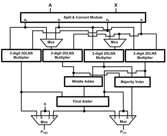
Using 11 bits to represent the binary-base exponent and 11 bits for the second-base expo-nent in a 2-digit 2DLNS representation, an acceptable mapping of 32-bit binary data has been achieved. In a one-level 2DLNS recursive multiplier structure, the binary operands are split into two parts, denoted by high and low sections. Each section is converted to its 2-digit 2DLNS equivalent representation and multiplication is performed by using four 2-digit 2DLNS multiplier modules. In this manner, the size of required look-up tables is smaller than would be required by a non-recursive structure, with the added advantage of fewer and shorter interconnects. The partial products are summed in two stages. In the middle adder, the two operands have the same range, while in the final adder, the operands need to be adjusted. Fig. 4.2 shows this structure. As shown, both the input and output data are in binary representations.
4.3
Two-level Recursion
Having the samen-bit operands, this time split into fourn/4-bit values:
X = n/X4−1
k=0
xk·2k+ n/X2−1
k=n/4
xk·2k+
3n/X4−1
k=n/2
xk·2k+ n−1 X
k=3n/4
xk·2k (4.5)
A= n/X4−1
k=0
ak·2k+ n/X2−1
k=n/4
ak·2k+
3n/X4−1
k=n/2
ak·2k+ n−1 X
k=3n/4
ak·2k
X andAmay now be written as:
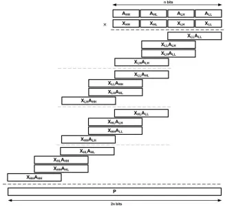
X =XHH+XHL+XLH+XLL , A=AHH +AHL+ALH +ALL (4.6)
and the multiplication ofAbyX will be:
P = A·X (4.7)
= (AHH +AHL+ALH +ALL)·(XHH+XHL+XLH +XLL)
= XHH·AHH +XHH·AHL+XHH ·ALH +XHH ·ALL
+ XHL·AHH+XHL·AHL+XHL·ALH +XHL·ALL
+ XLH·AHH+XLH ·AHL+XLH ·ALH +XLH ·ALL
+ XLL·AHH+XLL ·AHL+XLL·ALH +XLL·ALL
Now, the overall multiplication is reduced to sixteen smaller multiplications. As Fig. 4.3 shows, these partial products are summed to give the2n-bit final product. The partial
prod-ucts can be organized in four distinct groups, each group corresponds to one of the partial multipliers. This arrangement simplifies the overall design of the recursive multiplier ar-chitecture.
Figure 4.3: Two-Level Recursive Multiplier
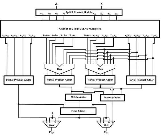
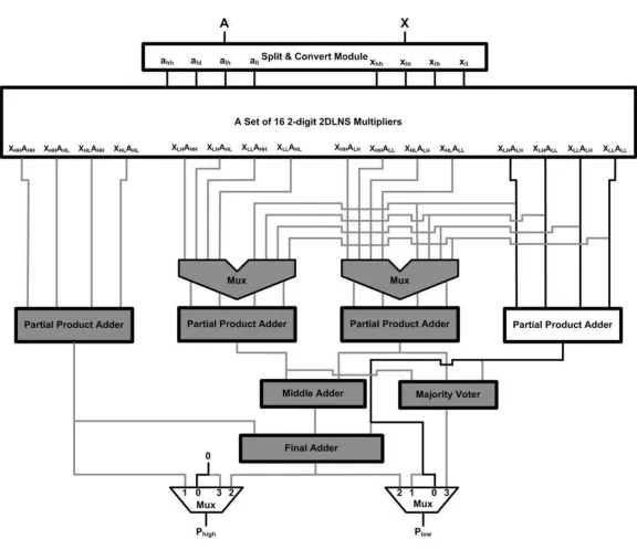
this architecture by splitting the high and low sections into two parts, where each part is converted to its equivalent 2-digit 2DLNS representation. A special module, called the partial product adder, has been implemented to produce the output of four resulting partial multipliers. Again, these values are summed using two stages of adders to arrive at the final result. Fig. 4.4 illustrates this architecture.
4.4
Synthesis Results and Comparison
Figure 4.4: The 2-digit 2DLNS-based Recursive Multiplier (Two-Level Recursion)
is mostly consumed by converters. The first architecture (Proposed-1) applies one level of recursion, and therefore acts on 32-bit values. In the second architecture (Proposed-2), with two levels of recursion, the size of RALUTs are much smaller than the first architecture, but more of them are required to realize the fully parallel structure. In our designs, both data conversion modules (Binary-to-2DLNS and 2DLNS-to-Binary), are used in parallel to convert all operands concurrently. Since as always there is a trade off between delay and area in these designs, for each 2DLNS converter, the serial version of the structure has been used, which is more appropriate for area-limited applications. A recursive digital multiplier architecture has been previously presented in [32], and includes a new column compression scheme to alleviate interconnection irregularity. Since this design has been implemented using TSMC-CMOS 0.18 µm technology, we can use it in a comparison study with the
in order to minimize the area, has been used to demonstrate the superiority of a recursive scheme ( with optimum level of recursion ) in terms of power consumption and speed.
Architecture
2DLNS-based 2DLNS-based 2DLNS-based Binary-based Synopsys Architecture Architecture Architecture Architecture Multiplier
(Proposed-1) (Proposed-2) (Proposed-2) [32]
Level of Recursion One Two Two One None
Technology STM-CMOS 90nm STM-CMOS 90nm STM-CMOS 90nm TSMC-CMOS 0.18µm STM-CMOS 90nm
Clock Frequency (MHz) 182 355 200 200
-Overall Area(µm)2 4,449,996 536,648 534,715 360,417 64,308
Dynamic power (mW) 15.39 10.01 4.86 582.31 62.72
Energy (mW/MHz) 0.085 0.028 0.024 2.912
-Data Arrival Time (ns) 5.25 2.57 4.71 8.51 35.52
Table 4.1: 64×64bit Recursive Multipliers Synthesis Results
archi-tectures we see that the 2DLNS-based structure, with an increase in area due to conversion, is about 45% faster while consuming 120 times less power. The clock frequency of this architecture can be increased up to 350 MHz, as shown in the third column of Table 4.1. Having this faster clock frequency adds about 0.36% to the area, which is negligible. How-ever, with a cost of doubling the power consumption, the delay is reduced by 1.8 times to 2.57 ns. Comparing this architecture with the binary-based architecture shows that with a 48% increase in area, delay is reduced 3.3 times and dynamic power is decreased 58.2 times. Therefore, both proposed architectures show excellent results in terms of delay and power consumption comparing to their binary counterpart. The Table 4.1 summarizes the synthesis results of these architectures.
4.5
Conclusions
In this chapter, two recursive 2DLNS-based multiplier architectures along with the perfor-mance results of their 64-bit implementations have been presented. These architectures benefit from 2DLNS properties, including more precise mapping of data and smaller size of data representations that lead to a reduction in hardware. Furthermore, since every mul-tiplication structure is conducted through 2-operand smaller size adders, no special column compression scheme is necessary. Contrary to binary structures, the recursion process in 2DLNS-based multipliers can be repeated as many times as needed to reach an optimum size for the look-up tables. In this regard, the second proposed architecture shows outstand-ing results as a low-power and high-speed multiplier. In recursive architectures, multipli-cation is carried out at maximum efficiency in terms of area, performance and power. The modern DSP processors provide optimistic context for the future of recursive architectures. The applications which will be discussed in the next chapters of this research work will benefit from these architectures.
Reconfigurable Multiplier Architectures
and dynamic power consumption.
5.1
Reconfigurable Architectures
We now discuss the application of two presented 2DLNS techniques in the previous chap-ter to the implementation of reconfigurable multiplier architectures in order to achieve im-proved performance under various conditions. Some modern hybrid architectures (such as controller/DSP chips) use variable width data buses which may lead to variable preci-sion arithmetic. If we use a fixed precipreci-sion arithmetic unit this will be inefficient in cases where the required precision is not the same as the fixed precision [32]. An example is the use of a fixed single precision unit to perform double precision arithmetic. Designing a reconfigurable hardware architecture definitely enhances the performance. Augmenting a data path with extra execution units provides computational parallelism, which increases processing performance and further provides an appropriate context for fault tolerant pro-cessing. The increasing complexity of electronic devices makes embedded fault detection and correction units a commercially wise decision. Checking hardware functionality is currently a more practical approach to fault tolerance [32]. The essence of fault tolerance lies in redundancy. Fault tolerance in our designs is realized through hardware redundancy when duplicate hardware implements parallel multiplication channels. Our new architec-tures combine the concepts of variable precision multiplication, high-speed and low-power design, fault tolerant computation, and high throughput arithmetic in one design.
5.2
Reconfigurable 2DLNS-based Multipliers
The 2-digit 2DLNS based recursive multiplier structures, presented in the previous chapter, are used as foundation blocks for the reconfigurable architectures.
re-Figure 5.1: The Reconfigurable 2-digit 2DLNS based Recursive Multiplier (One-Level Recursion)
configurable architecture may be of any size, merely with the restriction that the single precision mode must be exactly one half of the double precision mode, in our architectures all data widths, data buses and look-up tables have been designed for a 64-bit multiplication in double precision mode. The schematics of the reconfigurable architectures are provided in Fig. 5.1 and Fig. 5.2 corresponding to one and two levels of recursion respectively.
The architectures are regulated by a 2-bit control signalc1c0 to select one of the four
modes of operation. The bitc0 acts as the partial multiplier input selector for both
multi-plexers, while the complete control signal is used to select the lower and higher parts of the final output:
• Double Precision (64-bit) Multiplication (c1c0 = “10”)
Figure 5.2: The Reconfigurable 2-digit 2DLNS based Recursive Multiplier (Two-Level Recursion)
The outputs are summed in two stages of middle and final adders.
• Single Precision (32-bit) Multiplication (c1c0 = “00”)
For this mode, three of the base multipliers, in addition to the middle and final adders, half of the multiplexers and the majority voter circuitry are shut down. Since the final binary output is also partitioned, the higher portion is directly set to zero to avoid unnecessary transitions. In this case, the latency of the architecture is equal to that of the 2-digit 2DLNS multiplier or the partial multiplier, which leads to faster operation than in the double precision mode. The power reduction is important here because more than 75% of the hardware is disabled.
• Dual Single Precision Multiplication (c1c0 = “01”)
order bits of the bus. In this case, two of the base multipliers operate on two different sets of operands concurrently, while the remainder of the circuitry is inactive. This effectively doubles the system throughput, with the same latency as that of the single precision mode.
• Single Precision Fault Tolerant Multiplication (c1c0= “11”)
In this architecture, fault tolerance is realized through majority voting between three duplicate values. Here, three of the base multipliers are used in conjunction with a majority voter circuitry to form a simple single precision fault tolerant multiplier. The first level of multiplexers selects the appropriate signals as operands of the partial multipliers.
Figure 5.3: Double Precision Multiplier (One-Level Recursion)
Figure 5.5: Single Precision Multiplier (One-Level Recursion)
Figure 5.7: Dual Single Precision Multiplier (One-Level Recursion)
Figure 5.9: Single Precision Fault Tolerant Multiplier (One-Level Recursion)
5.3
Synthesis Results and Comparison
Two reconfigurable 64-bit 2-digit 2DLNS-based recursive multipliers have been imple-mented using STMicroelectronics CMOS 90nm process, facilitated by CMC Microsys-tems. The first architecture (Proposed-1) applies one level of recursion, and therefore acts on 32-bit values. The design circuitry include four 2-digit 2DLNS based multipliers, four multiplexers, two 64-bit and 128-bit adders, and a special majority voter module. At first, a split and convert module divides the 64-bit binary operands to two 32-bit values and then converts them to 2-digit 2DLNS representations. The Binary/2DLNS converters use look-up tables which consume about 90% of the overall area. In this design, again both data conversion modules (Binary-to-2DLNS and 2DLNS-to-Binary), are used in parallel to convert all operands concurrently; this would appear to be a reasonable trade off between chip area (and power) and speed, where high performance is the goal.
64×64bit 2DLNS-based 2DLNS-based 2DLNS-based Binary-based
Architecture Architecture Architecture Architecture Architecture
(Proposed-1) (Proposed-2) (Proposed-2) [32]
Level of Recursion One Two Two One
Technology 90nm 90nm 90nm 0.18µm
Clock Frequency (MHz) 200 350 200 200
Overall Area(µm)2 4,504,491 533,723 471,783 443,323
Dynamic Power (mW) 30.41 9.85 4.80 753.01
Energy (mW/MHz) 0.152 0.028 0.024 3.765
Data Arrival Time (ns) 4.75 2.63 4.73 9.00
Table 5.1: Reconfigurable Recursive Multipliers Synthesis Results
com-pressor distribution scheme in partial product reduction trees. This structure alleviates some of the problems associated with interconnection irregularities comparing to standard column compression multipliers, while avoiding the linear latency of array multipliers. Again, since this design has been implemented using TSMC 0.18µmCMOS standard cell
libraries, applying some scaling factors may be required. Although by scaling the tech-nology from 0.18µm to 90nm, a reduction in overall area, dynamic power and delay is
generally expected, the reduction factor for each figure is highly dependent on the design characteristics. In this design, the area utilization figure is calculated as 62.15% and 6 layers of metals are used [34], which shows that a considerable portion of the chip area is occupied by interconnects. In this case, scaling technology to 90nm does not affect area, power and delay figures considerably. This design is included to Table 5.1 and is used as a reference.
Our first architecture (Proposed-1) is 47% faster than its binary counterpart, and con-sumes 25 times less power. The second architecture (Proposed-2) includes two levels of recursion and acts on 16-bit words. The structure consists of the split and convert module, a set of sixteen 2-digit 2DLNS based multipliers, four partial product adders, four multiplex-ers, two 64-bit and 128-bit addmultiplex-ers, and again the majority voter module. Since the size of conversion tables depends on the size of the first and second base exponents, the RALUTs used in the binary to 2DLNS converters are almost 128 times smaller than the RALUTs used in the previous architecture. As we mentioned before, the number of RALUTs in this architecture is quadrupled, but we are still looking at a 32 times reduction to first order.
of doubling the power consumption; however, the delay is reduced by 1.8 times to 2.63 ns. Comparing this architecture with the binary-based architecture shows that with a 25% increase in area, delay is reduced by 29.2% and dynamic power is decreased 76.4 times.
Therefore, both proposed architectures show excellent results in terms of delay and power consumption comparing to their binary counterpart. Table 5.1 summarizes the syn-thesis results of these architectures and clearly shows the superiority of logarithmic based designs in terms of delay and power consumption. In particular, applying two levels of recursion allows the use of considerably higher clock frequencies.
5.4
Conclusions
Two reconfigurable recursive multiplier architectures have been presented, along with the performance results of their 64-bit implementations. The architectures benefit from both 2DLNS properties and recursive multiplications, which leads to a reduction in hardware. The architectures can be reconfigured in real time for both single and double precision arithmetic, as well as fault tolerant and dual single precision multiplications. Both single and double precision operations are carried out at the maximum efficiency in terms of area, performance and power. Modern DSP processors, such as those used in hand-held devices, may find considerable benefit from these high-performance, low-power, and high-speed reconfigurable architectures.
Finite Impulse Response (FIR) Filter
Design
6.1
FIR Filter Architecture
A digital filter uses a digital processor to perform numerical calculations on the sampled values of a signal. A FIR ( non-recursive ) filter is a digital filter whose output depends on the present and previous values of the input. The general difference equation for a FIR filter is:
Y[n] = N X
k=0
bk×X[n−k] (6.1)
whereY[n]is the filter output,X[n−k]is the filter input signal delayed byksamples,
andN is the order of the filter. The order of a FIR filter specifies the number of coefficients
and the number of iterations in the computations. FIR filters are simple to design, linear and guaranteed to be Bounded Input-Bounded Output (BIBO) stable. The order of an FIR filter is considerably higher than that of an equivalent Infinite Impulse Response (IIR) filter meeting the same specifications, which leads to higher computational complexity for the FIR filter. As it can be seen from the difference equation, each output sample depends on the previous N input samples which are multiplied by a set of coefficients, bks. Fig. 6.1 shows the systolic architecture for a FIR filter:
Figure 6.1: The Systolic Structure for a FIR Filter
The set of coefficients are generated based on the design specifications. These speci-fications are usually required in the frequency domain on magnitude response of the filter and in addition to the order of the filter and frequency range include the maximum pass band ripple and the minimum stop band attenuation, as it is shown in Fig. 6.2.
Figure 6.2: The Magnitude Response of a Band Pass Filter
coefficients around the intermediate point considered equal, a linear phase response is ob-tained. Furthermore, for relatively higher values of the order of filter, FIR filters have a low sensitivity to filter coefficient quantization errors. FIR filtering requires the use of in-ner product computations, which is based on Multiply and Accumulate (MAC) operations. When 2DLNS is applied to the implementation of a typical FIR filter, every multiplication is converted to addition or subtraction that greatly reduces the hardware complexity. In this chapter, a band pass FIR filter with the following specifications is implemented: The order of the filter is 74 and the frequency edges of the pass band are 2857Hz and 4KHz. The maximum allowed ripple in pass band is 0.01dB and the minimum attenuation required in stop band is 60dB. Based on the above design characteristics, the filter coefficients have been generated in MATLAB and then converted to 2’s complement binary representations. A chirp signal has been also generated in MATLAB to be applied to the filter architecture as the input signal. A chirp is a signal in which the frequency increases or decreases with time. In our sinusoidal chirp signal, the frequency increases from 0Hz to 8KHz in a 1 sec-ond time period.
results. Executing this program generates the corresponding output graphs.
6.2
16-bit Input Signal
In this case, the original values of both input signal and filter coefficients are 16-bit binary values. Here, the amplitude of the chirp signal is equivalent to 16-bit, 2’s complement binary representation. Fig. 6.3 shows this signal:
0 0.1 0.2 0.3 0.4 0.5 0.6 0.7 0.8 0.9 −3
−2 −1 0 1 2 3
x 104 Chirp Input
Signal (16−Bit)
Time (s)
Figure 6.3: The Filter Input Signal
If the 16-bit binary coefficients generated by MATLAB program along with this chirp signal apply to the MATLAB internal FIR filter functions, the worst case stop band attenua-tion is -60.5116dB and pass band ripple is +0.0119dB. The obtained stop band attenuaattenua-tion perfectly satisfies the design criterion, but the pass band ripple is slightly more than the specified value with an acceptable precision. However, we continue with this set of filter coefficients.
6.2.1
Binary-based Design
data are read from a file. A MAC structure operates on two sequences of data and coef-ficients, multiplies corresponding elements of the sequences and accumulates the sum of products in an optimized scheme. In this scheme (Optimized-1), in order to reduce the size of the product, firstly the sign bits of the operands are examined. The negative operands are converted to their positive 2’s complement representations and based on the sign of the product, it will be added to or subtracted from the accumulator. A sufficient number of extra bits have been considered in order to avoid overflow in accumulation. In order to show the efficiency of our optimized design, another binary-based filter has been designed, this time with the multiplier from the Synopsys internal library cells. Both designs are syn-thesized in their maximum speed, our design is also synsyn-thesized with the same frequency as of Synopsys design (Optimized-2):
FIR Filter Binary-based Binary-based Binary-based
Architecture by Synopsys Optimized-1 Optimized-2
Clock Frequency (MHz) 204 308 204
Overall Area(µm)2 672,860 639,471 469,019
Dynamic power(mW) 11.98 18.79 11.43
Data Arrival Time (ns) 4.70 3.03 4.69
Table 6.1: 16-bit Binary-based Designs Synthesis Results
As it is noticeable from the Table 6.1, the optimized design is advantageous in terms of VLSI area, delay, and maximum applicable clock frequency. Therefore, we will compare this design with the logarithmic filtering results at the end of this chapter.
0 0.1 0.2 0.3 0.4 0.5 0.6 0.7 0.8 0.9 −3
−2 −1 0 1 2 3
x 104 Filter Output for Chirp Input
Output Signal (34−Bit)
Time (s)
Figure 6.4: The Binary Filter Output Signal
6.2.2
2DLNS-based Design
Regarding the prior research in [31], considering 0.9202438884391765 as optimal second base in a 2-digit 2DLNS representation provides a good error-free mapping of 16-bit signed binary data. We have also considered 6 bits to represent the binary-base exponent for both input data and coefficients while to represent the second-base exponent for data and coefficients, 5 bits and 3 bits have been considered respectively. Here, the filter coefficient values are firstly converted to 2DLNS representations and then pre-stored in a coefficient memory. On the other hand, the input samples are converted to 2DLNS values during run time and then placed in a data memory. The main module in our 2DLNS design, which we will refer to asFilter, employs a couple of auxiliary modules through its external interface.
This structure is shown in Fig. 6.5.
The signal clk is the master clock signal that drives the Filter implementation. The
resetsignal is used to manage the whole operation of filtering. It resets all control signals
Figure 6.5: The Filter and Auxiliary Modules
file. The remaining connections of theFilterare its interface with the coefficient and data
memories. The signalscoef-mem-addressanddata-mem-addressprovide the addresses
to access memories. The coefficient memory contents are pre-stored and can only be read. The Data Memory has separate data lines to read data from memory, data-mem-data-in,
and to write data into memory, data-mem-data-out. Enable signals are used to enable
main module to access both memories, and the signal data-mem-write-enable is set by
the controller whenever data memory is accessed to be written.
At the Register Transfer Level (RTL) structure, theFiltermodule is composed of an Input
Register, a Binary/2DLNS Converter and its corresponding output register, a Multiply and Accumulate (MAC) unit, and a sequential Controller. The RTL level organization of the
Filtermodule is shown in Fig. 6.6.
Figure 6.6: The Filter RTL Components
done with the previous one and has asserted a ready signal to accept a new input sample. The output of the converter is transformed to an appropriate format by the converter output register in order to be stored into the data memory.
At the start of a filtering iteration, the source operands which are 2-digit 2DLNS values of input samples and coefficients are placed on the input ports of the MAC unit, and the operation commences. As it is shown in Fig. 6.7, the main part of the MAC architecture ac-tually is a sign-magnitude 2-digit 2DLNS multiplier, and another adder which is instructed by the control unit, accumulates the products in an iteration and forms the output signal. The MAC operation is accomplished in one clock cycle.
At the end of operation, the result is written into an output file. The control unit specifies the sequence and timing of the operations. The control ports of the data path component instances are connected to the control signals managed by the control unit. The output of this structure is shown in Fig. 6.8.
Figure 6.7: The MAC Unit Structure
consumption.
There are two 2DLNS-based FIR filterbank designs in literature [29] and [36]. In our design, the modified versions of 2DLNS/Binary conversions programs in [29] have been used. Table 6.2 shows some properties of these designs. This table also includes our 2DLNS-based design characteristics, when it is synthesized for a low clock frequency as 4.8 MHz. Since these designs both have been implemented using 0.18µmTSMC CMOS
0 0.1 0.2 0.3 0.4 0.5 0.6 0.7 0.8 0.9 −3
−2 −1 0 1 2 3
x 104 Filter Output for Chirp Input
Output Signal (20−Bit)
Time (s)
Figure 6.8: The 2DLNS Filter Output Signal
FIR Filter Architecture [29] [36] Proposed
The Order of the Filter 74 74 74
Technology CMOS TSMC 0.18µm TSMC 0.18µm STM 90nm
Clock Frequency (MHz) 4.8 4.8 4.8
Overall Area(µm)2 53,716 184,965 32,132
Dynamic power(µW) 316 708 34
Table 6.2: 2DLNS-based Designs Synthesis Results
6.2.3
Recursive 2DLNS-based Design
are doubled in this architecture. The output of these converters are placed in one word in the corresponding output register. Similarly, data values are stored in the data memory with the same pattern, four 2DLNS digits in each memory cell. In this architecture four parallel MAC units are required to perform MAC operations on 2-digit operands.
At the start of a filtering iteration, the source operands, which are four couple of 2-digit 2DLNS values of input samples and coefficients, are placed on the input ports of four MAC units, and the operation begins. The output result of these units are summed in two stages to yield the output of the iteration. The accumulator along with its corresponding register provide the final output of the MAC operation. This structure is shown in Fig. 6.9.
Figure 6.9: The MAC Unit Structure in Recursive Architecture
Since coefficients are pcomputed, sometimes the conversion hardware overhead re-garding the split coefficients may be excluded from the recursive design considerations. This way, while the input data are split, the genuine coefficients will be still applicable. In any case, the same optimal base should be used to represent both data and coefficients. This fact may impose some limitations to the recursive filter design. However, the recursive architecture has been implemented in two approaches:
• Split input data and split coefficients
then converted to 2-digit 2DLNS values and pre-stored in a look-up table, which we refer to as coefficient memory. Having split data and coefficients, the full structure of the MAC unit consisting of four parallel similar channels is utilized. The outputs of these channels should be shifted properly and summed up to yield the final product of each iteration. For this structure, 5 bits to demonstrate the binary index and 2 bits to represent the second base exponent are considered. The optimal base for this case is calculated as 0.8087001487814504. After addition of corresponding exponents, we will have 3 bits to represent the second base index. This time, the optimal base is calculated as 0.808750023022608 which is close enough to the previous value. Therefore, with a good approximation, we use the same second base for conversion to binary. The output of this structure is shown in Fig. 6.10. In this case, the average stop band attenuation is -65.0279dB and maximum pass band ripple is 0.0275dB.
0 0.1 0.2 0.3 0.4 0.5 0.6 0.7 0.8 0.9 1 −3
−2 −1 0 1 2 3
x 104 Filter Output for Chirp Input
Output Signal (36−Bit) (Split Coefficients)
Time (s)
Figure 6.10: The Recursive 2DLNS Filter (Split Coefficients) Output Signal
• Split input data and genuine coefficients
we consider the same configuration for conversion to 2DLNS values as of 16 bit case; 6 bits and 3 bits for binary and second base indices respectively. Since these values for data conversion are still 6 bits and 5 bits respectively, the same optimal base that is 0.9202438884391765 can be used for both conversions. Having genuine coefficients, two of the channels in MAC unit are eliminated. Furthermore, there are some reduction in the adder stages of the MAC unit. The output of this structure is shown in Fig. 6.11. In this case, the average stop band attenuation is -79.0385dB and maximum pass band ripple is 0.0130dB.
0 0.1 0.2 0.3 0.4 0.5 0.6 0.7 0.8 0.9 1 −3
−2 −1 0 1 2 3
x 104 Filter Output for Chirp Input
Output Signal (28−Bit) (Genuine Coefficients)
Time (s)
Figure 6.11: The Recursive 2DLNS Filter (Genuine Coefficients) Output Signal
6.2.4
Synthesis Results and Comparison
design. If this design is synthesized with a clock frequency of 250 MHz, both area and power will be reduced to 513,743(µm)2 and 14.36(mW)respectively, but delay will be
increased to 3.79 ns. This way, the 2DLNS-based design consumes about 14% area and 34% power as that of the binary-based architecture, when both running in a clock frequency of 250 MHz.
FIR Filter Binary-based 2DLNS-based Recursive Recursive
Architecture 2DLNS-based 2DLNS-based
Split Coefficients Genuine Coefficients
Clock Frequency (MHz) 308 256 188 189
Overall Area(µm)2 639,471 72,941 65,606 118,913
Dynamic power(mW) 18.79 5.26 7.10 6.62
Energy(mW/M Hz) 0.061 0.021 0.038 0.035
Data Arrival Time (ns) 3.03 3.70 5.13 5.05
Data Representation (bit) 16 2×(1,6,5) 2×2×(1,5,2) 2×2×(1,6,5)
Coefficient Representation (bit) 16 2×(1,6,3) 2×2×(1,5,2) 2×(1,6,3)
Table 6.3: 16-bit FIR Filter Designs Synthesis Results
and consequently data can not be converted to 2DLNS values with a smaller representation. In recursive architectures area and power are more than we expected due to an increase in interconnections. Therefore, using recursive architectures has no added advantage in this case.
Nevertheless, the synthesis results show the superiority of 2DLNS-based design in terms of VLSI area and power consumption and confirm that 2DLNS is the platform of choice for low-power FIR filter design. It seems the recursion process in 2DLNS arithmetic yields the maximum efficiency whenever it practically leads to smaller size data representations and conversion RALUTs. In order to resolve this problem with recursive designs in this application, the 32-bit architectures will be implemented in the next section.
6.3
32-bit Input Signal
Here, the amplitude of the chirp signal is equivalent to 32-bit, 2’s complement binary rep-resentation. Fig. 6.12 shows this signal. This signal will be applied to the four FIR filter architectures which are modified to work on 32-bit data and coefficients.
0 0.1 0.2 0.3 0.4 0.5 0.6 0.7 0.8 0.9 −2
−1.5 −1 −0.5 0 0.5 1 1.5 2
x 109 Chirp Input
Signal (32−Bit)
Time (s)