Design and Implementation of Central
Processing Unit based Programmable
Reversible Gate
Shachchidanand Nagagach, Deepak Kumar
M. Tech. Scholar, Department of Electronics and Communication Engineering, Vidhyapeeth Institute of Science & Technology, Bhopal, India
Assistant Professor, Department of Electronics and Communication Engineering, Vidhyapeeth Institute of Science & Technology, Bhopal, India
ABSTRACT: Reversible computing spans computational models that are both forward and backward deterministic. These models have applications in program inversion and bidirectional computing, and are also interesting as a study of theoretical properties. A reversible computation does, thus, not have to use energy, though this is impossible to avoid in practice, due to the way computers are build. It is, however, not always obvious how to implement reversible computing systems. The restriction to avoid information loss imposes new design criteria that need to be incorporated into the design; criteria that do not follow directly from conventional models.
In this paper, investigate garbage-free reversible central processing unit computing systems to physical gate-level implementation. Arithmetic operations are a basis for many computing systems, so a proposed the design of adder, sub tractor, multiplexer, encoder and work towards a reversible circuit for general circuit are important new circuits. In all design implemented Xilinx software and simulated VHDL text bench.
KEYWORDS: Reversible Gates, Central Processing Unit (CPU), Ancilla Input, Delay
I. INTRODUCTION
controlling single Quantum systems have been developed. For example, methods have been developed for trapping a single atom in an ‘atom trap’, isolating it from the rest of the world and allow us to probe many different aspects of its behavior with incredible precision [4]. Quantum computation and Quantum information provide a useful series of challenges at varied levels of difficulty for people devising methods to better manipulate single quantum systems, and simulate the development of new experimental techniques. The ability to control single quantum systems is essential if we are to harness the power of quantum mechanics for applications to Quantum computation and Quantum information. Despite this intense interest, efforts to build Quantum information processing systems have resulted in modest success to date. Small Quantum computers, capable of doing dozens of operations on a few qubits represent the state of the art in Quantum computation. However, it remains a great challenge to physicists and engineers to develop techniques for making large-scale Quantum information processing a reality [5].
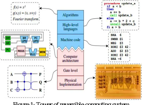
Figure 1: Tower of reversible computing system
In his 1961 paper, Landauer wrote that “we shall label a machine as being logical reversible, if and only if all its individual steps are logically reversible” [6]. This is a very grand challenge and we know from Bennett (and later work) that, theoretically, such machines do exist – even when we add the requirement that the final result must not include garbage. But is it possible to realize such machines in practice and can it is done with the fabrication technology that exists today? And will we actually be able to achieve the expected reduced heat dissipation? The MicroPower research project [7], which started in 2009, has as objective to develop a proof-of-concept reversible computing system and the computer science theory behind it. To do this all parts of the reversible computation tower (Figure 1.1) must be investigated. More specifically, the project investigates whether reversible computing can be applied in a power-limited application (specifically hearing aids) with the future hope to either reduce power consumption or increase functionality [8].
II. ARITHMETIC LOGIC CIRCUITS
garbage bit. Several reversible adder designs used this ripple structure; e.g. reversible binary-coded decimal adders have received some interest.
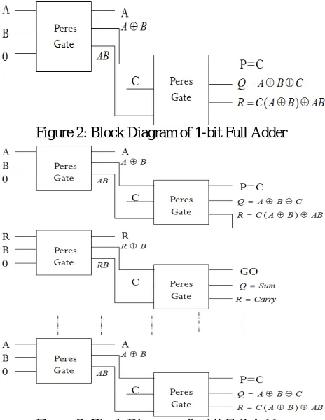
Figure 2: Block Diagram of 1-bit Full Adder
Figure 3: Block Diagram of n-bit Full Adder
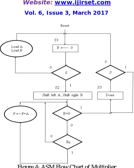
Figure 4: ASM Flow Chart of Multiplier
Multimedia transforms are an interesting application area for reversible circuits. In small battery-powered devices (e.g. smartphones and mp3-players) they are often included as part of an ASIC to reduce power consumption and a key property of many such transforms is that they are information-lossless (and thus invertible). There exist many application areas of such transforms and even the earliest quantum algorithms make use of a quantum implementation of the Fourier transform. Also a implementation of the fast Fourier transform in reversible logic has been investigated.
Figure 6: Proposed Diagram of 4×1 Multiplexer
The first approach to reversible logic synthesis is actually a very beautiful example of how mathematics can be related to reversible circuits. Based on work by Rayner and Newman, Storme and De Vos used that reversible gates and cascading of these by serial composition forms a group, with the result that it is possible to use the known methods from group theory. Specifically, one of these methods can be used to decompose an arbitrary reversible circuit into a cascade of simpler circuits that only updates one input wire.
Figure 7: Proposed 1-bit Memory Store Element
Reversible logic synthesis have since been much researched and often with an interest to also apply the methods to quantum circuits. Many of the approaches is based on techniques known from Boolean logic synthesis. There exists many more, but common to these are that they are based on truth tables as input and that they actually try to solve an NP-hard problem.
According to base paper, the use different technique used for central processing unit (CPU) using arithmetic logic unit (ALU) and different types of reversible logic gate. In base paper generally concentrate on the number of slice (area), number of look up table (LUT) and maximum combination path delay (MCPD) of the central processing unit. In this dissertation proposed central processing unit based TR gate and used to multiplier, adder, sub tractor, multiplexer and encoder. So step by step explain proposed design is below:
Layout the data bus to handle all of the operations of the reversible CPU. Design the reversible realizations of the flip-flops.
Design the reversible memory circuits (such as buffer registers and counter circuits) using the proposed reversible flip-flops of the previous step.
Design the arithmetic circuits such as adder, multiplier, divider, comparator etc. Design the reversible realization of ALU.
Design the reversible control unit of the processor by designing an efficient instruction decoder.
III. SIMULATION RESULT
More specifically, we have developed new garbage-free circuits for addition and are working towards a general multiplication circuit. We have also combined multiple operations together to implement a reversible arithmetic logic unit. With these and other garbage-free arithmetic circuits it is possible to design larger reversible computing systems. As an example, we have implemented discrete lossless transforms by redesigning these with a lifting scheme. We have also shown the design of a reversible computing architecture and implemented this using only reversible logic gates. While, these are still small systems, with further development it should be possible to use similar strategies to implement even larger systems.
From our own design experience, we know that designing logic gate-level circuits quickly becomes complicated when the functionality and number of wires involved are increased. To make the design process easier, we have developed two hardware description languages. Using examples from known reversible circuits, we have shown that circuits can be described reasonably concisely. These are, however, still small examples and we need to implement a larger system to show the usefulness of the languages.
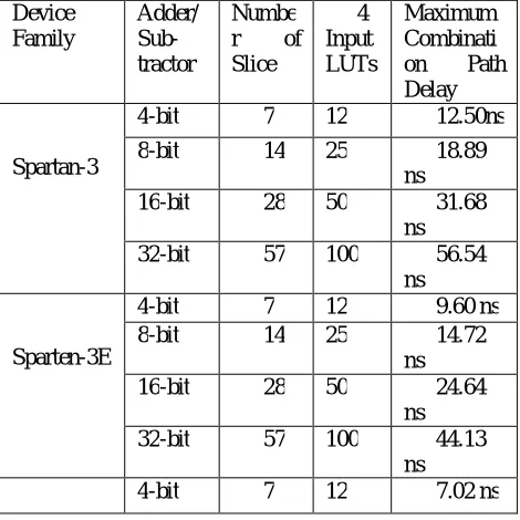
Table 1: Syntheses Result for Reversible 4-bit, 8-bit, 16-bit and 32-bit Adder/Sub tractor with different Device Family Device Family Adder/ Sub-tractor Numbe r of Slice 4 Input LUTs Maximum Combinati on Path Delay
Spartan-3
4-bit 7 12 12.50ns
8-bit 14 25 18.89
ns
16-bit 28 50 31.68
ns
32-bit 57 100 56.54
ns
Sparten-3E
4-bit 7 12 9.60 ns
8-bit 14 25 14.72
ns
16-bit 28 50 24.64
ns
32-bit 57 100 44.13
ns
Spartan-6
8-bit 14 25 9.55 ns
16-bit 28 50 14.50
ns
32-bit 57 100 24.17
ns
Figure 9: RTL view of 4-bit Adder/Sub tractor
Figure 11: Output waveform of the 4-bit Adder/ Sub-tractor Circuit
Figure 12: Output waveform of the 32-bit Adder/ Sub-tractor Circuit
Figure 13: Timing Summary of 32-bit Adder/ Sub-tractor in Spartan-6 device family Table II: Comparative Results of Existing Algorithm and Proposed Algorithm in 4-bit
Parameter 4-bit Reversible
Full Adder [1]
Reversible FA using
Peres Gate
4-bit Reversible
Full Sub tractor [1]
Reversible FS using TR Gate
AI 12 4 12 4
GO 8 8 8 8
QC 72 32 80 48
Delay 66 48 66 40
Figure 14: Bar Graph of the Previous and Proposed Reversible Full Adder
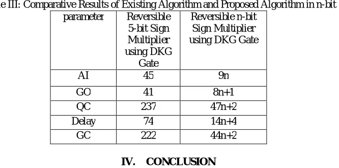
Figure 15: Bar Graph of the Previous and Proposed Reversible Full Adder Table III: Comparative Results of Existing Algorithm and Proposed Algorithm in n-bit
parameter Reversible 5-bit Sign Multiplier using DKG
Gate
Reversible n-bit Sign Multiplier using DKG Gate
AI 45 9n
GO 41 8n+1
QC 237 47n+2
Delay 74 14n+4
GC 222 44n+2
IV. CONCLUSION
REFERENCES
[1] Lafifa Jamal and Hafiz Md. HasanBabu, “Design and Implementation of a Reversible Central Processing Unit”, 2015 IEEE Computer Society Annual Symposium on VLSI 2015 IEEE.
[2] Md. Shamsujjoha and Hafiz Md. HasanBabu, “A Low Power Fault Tolerant Reversible Decoder Using MOS Transistor”, 2013 26th International Conference on VLSI Design and the 12th International Conference on Embedded Systems.
[3] Michael Nachtigal, and NagarajanRanganathan, “Design and Analysis of a Novel Reversible Encoder/Decoder”, 2011 11th IEEE International Conference on Nanotechnology Portland Marriott August 15-18, 2011, Portland, Oregon, USA.
[4] Noor MuhammedNayeem, Md. Adnan Hossain, Md. MutasimulHaque, Lafifa Jamal, Hafiz M. HasanBabu, “Novel Reversible Division Hardware”, 978-1-4244-4480-9/09/$25.00 ©2009 IEEE.
[5] Matthew Morrison and NagarajanRanganathan, “Design of a Reversible ALU based on Novel Programmable Reversible Logic Gate Structures”, 2013 IEEE Computer Society Annual Symposium on VLSI.
[6] LekshmiViswanath and Ponni. M, “Design and Analysis of 16 Bit Reversible ALU”, ISSN: 2278-0661 Volume 1, Issue 1 (May-June 2012), PP 46-53
[7] Akanksha Dixit and VinodKapse, “Arithmetic & Logic Unit (ALU) Design using Reversible Control Unit”, International Journal of Engineering and Innovative Technology (IJEIT) Volume 1, Issue 6, June 2012.
[8] Mr. Abhishek Gupta, Mr. UtsavMalviya and Prof. VinodKapse, “Design of Speed, Energy and Power Efficient Reversible Logic Based Vedic ALU for Digital Processors”, 2012 IEEE Computer Society Annual Symposium on VLSI.
[9] H. Thapliyal and N. Ranganathan, "A New Reversible Design of BCD Adder," To appear in Proc. Design Automation and Test in Europe (DATE), 2011.