Copyright to IJIRSET DOI:10.15680/IJIRSET.2017.0607136 13736
Hardware Implementation of SEPIC based
LED driver using Hysteresis current controller
Jeevan Kishore N
1, Raghumanth A
2, Dr.Venugopal N
3P.G. Student, Department of Electrical Engineering, PESIT College, Banashankari, Bengaluru, India1
Associate Research Fellow, Department of Electrical Engineering, PESIT College, Banashankari, Bengaluru, India2
Professor, Department of Electrical Engineering, PESIT College, Banashankari, Bengaluru, India3
ABSTRACT:Nowadays the LED’s are effectively dominating and replacing the usage of traditional incandescent and
fluorescent lighting devices in commercial and domestic applications due to their higher efficiency, low power consumption, flicker free operation and longer life. In order to enhance the higher efficiency and longer life of this LED’s, the lower ripple current and performance improvement is obtained by controlling the output current with suitable current controller technique. This paper aims at hardware implementation of a SEPIC based LED driver with Hysteresis controller for constant output current with lower ripple current. The SEPIC converter can be used for wide variation in the input voltage where usually fed from the battery source. At present this type of converters are being used as the SMPS with higher switching frequency which reduces the filter size and the efficiency of the converter can be improved. In this paper the hardware implementation of 10 W prototype SEPIC converter using Hysteresis controller has been done with switching frequency of 20kHz.
KEYWORDS: SEPIC; Hysteresis controller; SMPS;LED’s.
I. INTRODUCTION
In order to save the energy and to have advancement in the field of green energy industry, and also taking the environment friendliness into the account Light Emitting Diode(LED) is widely used in domestic and commercial lighting applications. So the traditional incandescent and fluorescent lights are replaced by the LED lamps. A light emitting diode is a two terminal semiconductor light source. High brightness LED’s are spreading all over the lighting application due to its longer life and less power consumption. But the life of LED based lamps mainly depends on the life of the driver integrated with it. So a high performance converter is required to produce low ripple with constant output current.
The forward operating current of typical high bright LED is found to lie between 0 to 350mA and forward voltage drop Of 3.2 volts. In order to obtain the sufficient illumination number of LED chips are connected in series or parallel combination depending on the driver used. The illumination of these LED chips connected in series or parallel main depends on the forward current of the LED’s. So the brightness can be controlled by varying the current but usually the LED’s are driven with constant current with reduced ripple, this can be done by using the converter with small size and less EMI. Various topologies have been used, but these converters have their own pro’s and con’s.
Copyright to IJIRSET DOI:10.15680/IJIRSET.2017.0607136 13737
A hysteresis controller is used here to controller the SEPIC converter in closed loop operation. In this controller the actual value of input current is compared with the reference value and the resultant error signal is given to the hysteresis band which maintains the current within the hysteresis band using the switch.
II. BLOCKDIAGRAM
(a)
Typical Block diagram of the proposed SEPIC LED driver using Hysteresis is as shown in Fig1 (a).
1. Battery-Is used as the source of energy to drive the LED strings.
2. SEPIC converter-The stored energy in the battery is used as input to the converter to have desired output
voltage and current.
3. LED-This project mainly aims on the lighting applications, so the LED’s is used as the load.
4. Hysteresis controller-Basically the LED should be operated with constant current so this is achieved using
hysteresis controller.
III. CIRCUITDIAGRAMANDMODESOFOPERATION
SEPIC converter – It is one of the DC -DC converter which is capable of operating in step down mode or step up mode depending on the duty cycle of gate signal and modes of operation is as follows.
MODE 1-Fig (b) shows the switch turn ON i,e When switch S is closed then current ILi increases and the current ILo
also increases in the negative direction. Since S is a short while closed then instantaneous Voltage VCi is
approximately VS and the voltage VLo is Approximately -VS. Therefore, the capacitor supplies the energy to
Copyright to IJIRSET DOI:10.15680/IJIRSET.2017.0607136 13738
(b)
Mode 2- Fig (c) shows the switch turn OFF i,e When switch S is open then current which flows in the capacitor Ci i.e
Ici becomes the same as the current ILi . The current will continue in the negative direction. It can be seen from the
diagram that a negative ILo will add to the current to increase the current ILi delivered to the load. Then S is off, power
is delivered to the load from both Lo and Li. Ci however is being charged by Li during this off cycle, and will in turn
recharge Lo during the on cycle.
(c)
IV.MATHEMATICALDESIGN
Duty cycle of the SEPIC converter is given by
D=Vo/(Vin+Vo)
Inductor Selection is done by,
Iripple = Iout * Vo/Vin *40%
Iout = P/Vo
L1=L2=L=Vin/(Iripple*fs)*D
IL1(peak) = Iout * Vo/Vin*(1+ (40%)/2)
IL2(peak) = Iout * (1+ (40%)/2)
Coupling capcitor selection is given by,
ICS(rms) = IOUT *Sqrt(VO/Vin)
Copyright to IJIRSET DOI:10.15680/IJIRSET.2017.0607136 13739
ΔVCS = (Iout*D)/(Cs*fs)
Output capacitor selection is given by,
Cout ≥ (Iout*D)/(Vripple*0.5*fs)
ICout(rms) = Iout*sqrt(Vo/Vin).
V. CONTROLSTRATERGY
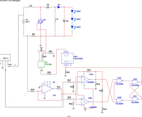
Figure (d) shows the schematic circuit diagram of proposed SEPIC based LED driver using Hysteresis current controller technique.
(d)
Hysteresis controller-Basically the LED should be operated with constant current control so this is achieved using hysteresis controller. There are many control technique, but Hysteresis current control is very much efficiently used in non linear and time variant systems. A hysteresis controller is used to control the output current of SEPIC converter during closed loop operation.
U1A 74LS00D U1B 74LS00D U1C 74LS00D U1D 74LS00D U2 741 3 2 4 7 6 5 1 U3A LM339N 5 4 3 2 12 U3B LM339N 7 6 3 1 12 U4A 74LS244N 1Y1 18 1Y2 16 1Y3 14 1Y4 12 1A1 2 1A2 4 1A3 6 1A4 8 ~1G 1 U5 TLP250
1 2 3 4
Copyright to IJIRSET DOI:10.15680/IJIRSET.2017.0607136 13740
In this technique, the controller uses PI with hysteresis block which controls the PWM signal to the MOSFET switch for a desired output current. The actual value of the converter output current is compared with output of PI controller and resultant error signal is again fed back to hysteresis block. The output current of converter is limited with in hysteresis band using the comparators.
In hardware implementation the input inductor current is sensed using a very low value of resistor R9. This feedback is connected to the 741 op-amp with some gain values and pin number 7 of the op-amp is connected to a 12V battery source. Then this signal is amplified with some gain value and compared with hysteresis band. The output of the Hysteresis is set by pots connected to LM339 comparator. Then comparator output is fed to S-R flip flop which latches output of the comparator which provides set pulse and reset pulse. Whenever the error is greater than the limit given in the hysteresis, the pulse goes high which is enabled by S-R flip flop by giving a set pulse. When the error signal is below the limit then the pulse is made low which is disabled by SR flip flop by giving a reset pulse which results in maintaining a constant output current of the SEPIC converter.
Further the set output pin of flip flop is connected to the buffer IC (LM7422N) in order to avoid the loading effect that reflects on to the circuit. Then output of buffer IC is fed to the driver IC TLP250 which has a unique feature with inbuilt opto-coupler providing isolation between MOSFET switch and controller. The generated closed loop PWM signal is fed to SEPIC converter MOSFET.
VI.SEPIC CONVERTER SPECIFICATION AND DESIGN PARAMETERS
Input voltage : 6 -12 V
Output voltage : 35 V
Output ripple voltage : 5% of Vo
Output current : 0.3 A
Output ripple current : 40% of Io
LED voltage drop : 3.2 V
LED rated current : 0.35 A
Duty cycle : 75-85%
Switching frequency : 20kHz
VII. EXPERIMENTAL RESULTS
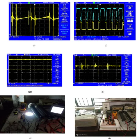
Figures shows the results of SEPIC converter output by using Hysteresis based current controller. The fig (e),(f),(g) and (h) shows charging and discharging of the input inductor current during switching of MOSFET. The PWM signal and voltage across the drain and source during switching of MOSFET of SEPIC converter, the output voltage of SEPIC converter with reduced ripple output voltage and current respectively.
Copyright to IJIRSET DOI:10.15680/IJIRSET.2017.0607136 13741
VIII.
(g) (h)
(i) (j)
Figure (i) and (j) shows the hardware implementation of SEPIC converter with LED load and Resistive load to verify the constant current for different values of load variation respectively.
Copyright to IJIRSET DOI:10.15680/IJIRSET.2017.0607136 13742
VIII CONCLUSION
In this particular project the stored energy in the battery is utilized to drive the LED with hysteresis current controlled SEPIC converter by boosting the 12 V to 35 V of output voltage as mainly LED operate with constant current. The implemented hardware prototype provides constant current with variation in output voltage, shown in fig (k) when load is varied from 100% to 50% the current remains same with value of 0.27 A.
(k)
REFERENCES
[1] de Britto J.R, Demian A.E., de Freitas L.C., Farias V.J., Coelho E.A.A.,Vieira J.B., A proposal of Led Lamp Driver for universal input using
Cuk converter, IEEE Power Electronics Specialists Conference, PESC(Print ISBN: 978-1-4244-1667-7 ), Rhodes Island, pp. 2640 - 2644,2008.
[2] Cheng Y.K., Cheng K.W.E., General Study for using LED to replacetraditional lighting devices, Power Electronics Systems and Applications
Conference, IPCSA (Print ISBN: 962-367-544-5), Hong Kong, pp.173 - 177, 2006.
[3] Doshi Montu, Zane Regan, Digital Architecture for Driving Large LEDArrays with Dynamic Bus Voltage Regulation and Phase Shifted PWM,
Applied Power Electronics Conference, APEC (Print ISBN: 1-4244-0713-3), Anaheim - CA, pp. 287 - 293, 2007.
[4] Chen C.C., Wu C.-Y., Wu T.-F., LED back-light driving system for LCDpanels, IEEE Twenty-First Annual Conference and Expositions on
Applied Power Electronics, APEC (Print ISBN: 0-7803-9547-6), 2006.
[5] Xiaoru Xu, Xiaobo Wu High dimming ratio LED driver with fast transient boost converter, IEEE Power Electronics Specialists Conference,
PESC (Print ISBN: 978-1-4244-1667-7), Rhodes Island, pp. 4192 -4195, 2008.
[6] van der Broeck Heinz, Sauerlander Georg, Wendt, Matthias, Power driver topologies and control schemes for LEDs, IEEE Twenty-second