Comparative Analysis of Three-Leg Single DC
Link Capacitor Based DSTATCOM with Split
Capacitor Based DSTATCOM
J.Jerin Asir1, M. Balasubramanian2
PG Scholar, Department of Electrical Engg., Government College of Engineering, Tirunelveli., India 1 Assistant Professor, Department of Electrical Engg., Government College of Engineering, Tirunelveli., India 2
ABSTRACT: This paper proposes a comparative analysis between a three leg split capacitor based DSTATCOM and a
three leg single dc link capacitor based DSTATCOM. In both the topologies the DSTATCOM is coupled to the line by means of an interfacing inductor which acts as a filter. The major drawback associated with the split capacitor based DSTATCOM is the voltage unbalancing issue across the split capacitors at the front end of DSTATCOM. To overcome the above mentioned voltage unbalancing issue another topology is introduced named as single dc link capacitor based DSTATCOM. In this topology the split capacitors are converted into a single dc link capacitor, so that the voltage unbalancing issue associated with the split capacitor based DSTATCOM is avoided. Simulation studies for both the topologies are carried out and its results are presented.
KEYWORDS:Distribution Static Compensator (DSTATCOM), Voltage Source Inverter (VSI), Instantaneous
Symmetrical Component Theory (ISCT), Hysteresis Band Current Controller (HBCC), Proportional Integral (PI) Controller.
I. INTRODUCTION
fourth leg is mainly used to compensate the neutral current, so that it is connected to the line neutral. This topology is explained further in [4,5]. The main drawback of this topology is the usage of more number of VSI switches which will result in more switching losses. Three single phase VSI based DSTATCOM topology has three single phase VSIs which is connected back to back. In this topology, each single phase VSI is responsible for the compensation of each single line in the system. Here, the DSTATCOM structure is connected to the line by means of a coupling transformer. The detailed view of this topology is explained in [1,6]. The split capacitor based DSTATCOM topology uses a three leg VSI with the split dc link capacitors at its front end. In order to compensate the neutral current the source neutral and load neutral are connected to the mid-point of the split capacitors. This topology has the advantage of using less number of VSI switches and independent control of VSI legs. This topology is further explained in [7,8]. The split capacitor based DSTATCOM topology has one serious problem associated with it. Since, it is using the split capacitors there is a voltage unbalancing issue across the capacitors which will results in unequal capacitance leakage currents, unequal delays in the switching devices, charging of capacitors is asymmetrical during transients. However when the load current contains a dc component, the voltage unbalance between the capacitors becomes very high. The problems due to the voltage unbalance is discussed in [9,10]. In order to avoid the unbalancing issue some additional circuitry is needed. However it will increase the overall cost of the system. It is further explained in [11,12].
The next DSTATCOM topology is single dc link capacitor based DSTATCOM. The detailed explanation of this topology is given in [13]. In order to avoid the voltage unbalancing issue associated with the split capacitor based DSTATCOM the split capacitor is converted into a single dc link capacitor. At the same time in order to compensate the neutral current an additional small ac capacitor is connected between the negative of the dc bus and the system neutral. The comparison between the split capacitor based DSTATCOM and single dc link capacitor based DSTATCOM is explained below.
Both the topologies uses the same control algorithms. (i) Instantaneous symmetrical component theory (ISCT) [14] to generate the reference currents. (ii) Hysteresis band current controller (HBCC) [15] to generate the pulses forthe VSI switches. The steady state and transient performance of both the topologies for three-phase four-wire distribution system is explained through simulation studies.
II. STRUCTURAL COMPARISON BETWEEN THREE LEG SPLIT CAPACITOR BASED DSTATCOM AND SINGLE DC LINK CAPACITOR BASED DSTATOM
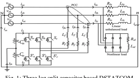
Fig. 1: Three leg split capacitor based DSTATCOM
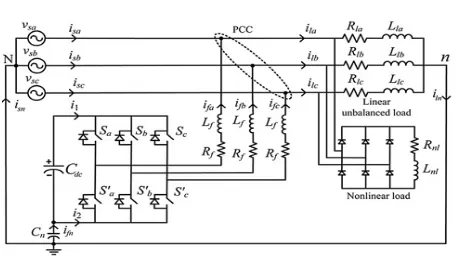
Fig. 2: Three leg single dc link capacitor based DSTATCOM
Fig 2 represents the three leg single dc link capacitor based DSTATCOM. In this topology instead of using split capacitors before the DSTATCOM, a single dc link capacitor is used. At the same time to compensate the neutral current, a small ac capacitor is connected between the negative of the dc bus and the system neutral. This is the structural difference between the two topologies.
III. DESIGN OF TWO DSTATCOM TOPOLOGIES
A. Design of split capacitor based DSTATCOM
The parameters to be considered while designing are, (i) DC link voltage (Vdc) (ii) DC storage capacitor (Cdc) (iii)
Interfacing inductance (Lf) (iv) Switching frequency (Fsw) A.1 DC link capacitor value (Cdc)
It is given by,
= ( . )
( . ) (1)
where, X is the DSTATCOM KVA rating, Vmis the peak value of source voltage,T is the time period of each cycle,n is
the number of cycles.
A.2 Interfacing inductance (Lf)
It is given by,
= . (2)
Where, ℎ= ( ) (3)
K1, K2is the proportionality constants. Fswmaxis the maximum switching frequency. Fswminis the minimum switching
frequency. m is given by,
=
( )
(4)
A.3 DC link voltage (Vdc)
The voltage reference (Vdcref) of DC link capacitopr has been taken as 1.6Vmfor each capacitor. B. Design of single dc link capacitor based DSTATCOM
The parameters to be considered are, (i) Neutral capacitor (Cn) (ii) DC link voltage (Vdc) (iii) DC link capacitor (Cdc)
B.1 Neutral Capacitor (Cn)
In order to find out Cn, we need to equate the phase ‘a’ filter current and phase ‘a’ load current. This is done, because
the filter sends the compensating current into the line to balance the load (i.e) making the source current as a balanced sinusoidal one.
The load current for ‘a’ phase is given by,
=
( ) (5)
The filter current for ‘a’ phase is given by,
=
( ) (6)
where, Vsa is the phase ‘a’ source voltage, Rla and Xla is the phase ‘a’ load resistance and reactance, Rf and Xfis the
filter resistance and reactance, V1 is the fundamental inverter output voltage, Xcn is the reactance of neutral capacitor.
By equating the imaginary parts of equations (5) and (6),
( )
( )=
( )
( ) ( − ) (7)
By applying all the known values in equation (7), the value of neutral capacitor (Cn) can be found out.
B.2 DC link voltage (Vdc)
As discussed in the split capacitor based DSTATCOM topology, we need to maintain a dc link voltage of 1.6Vm. In
this topology, only one dc capacitor is used. So the reference voltage (Vdcref) to be maintained across the capacitor is
(2*1.6Vm).
B.3 DC link capacitor (Cdc)
The functions of DC capacitor in the DSTATCOM are to (i) maintain the dc voltage with minimum ripple during steady state (ii) act as an energy storage element to supply reactive and harmonic power of the load.
It is given by,
=
( . ) ( . ) (8)
B.4 Filter inductance (Lf)
It influences (i) switching frequency (ii) rate of change of filter current. It is given by,
= . (9)
Where, Fmaxis the maximum switching frequency, h is the width of the hysteresis band. A proper hysteresis band (±ℎ)
is to be selected for better tracking performance. Normally, the band width is selected as 5% of the compensator current.
IV. CONTROL ALGORITHM
It is common for both the DSTATCOM topologies. The steps to be followed are, (i) Generate the reference filter currents (i*fabc).
(ii) Compare the reference filter currents (i*fabc) with the actual filter currents (ifabc) and generate the pulses for VSI
switches.
(iii) Maintain the dc link voltage (Vdc) at a reference value (Vdcref) with the help of PI controllers. Step 1: Generate reference filter currents (i*fabc)
It is generated by using Instantaneous Symmetrical Component Theory (ISCT). It is given as,
∗ = − ( )
∗ = − ( )
∑ , , ( + ) (11)
∗ = − ∑ ( )
, , ( + ) (12)
where, (ila, ilb, ilc) represents the three phase load currents, (Vsa, Vsb, Vsc) represents the three phase source voltages, Pl
is the average load power, Ploss represents the switching and ohmic losses in the actual compensator. = √ . Φ is
the desired phase angle between source voltage and current. In order to obtain unity power factor (UPF), the value of β
was chosen as zero.
Average load power (Pl) is given by the equation,
= ∫ ( + + ) (13) Ploss is given by the equation,
= + ∫ (14)
where, evdc = Vdcref – Vdc. (i.e) the error difference between reference dc link voltage and actual dc link voltage, Kp is
the proportional gain, Ki is the integral gain. Step 2: Generate the pulses for VSI switches
In order to generate the pulses for VSI switches, a Hysteresis Band Current Controller (HBCC) technique is used. The switching control law is given as,
(i) If ifa≥ i*fa + h, then bottom switch is turned ON whereas the top switch is turned OFF. (Ua = 0, Ua = 1).
Ua denotes all the VSI top switches.
Ua denotes all the VSI bottom switches.
(ii) If ifa≤ i*fa – h, then bottom switch is turned OFF whereas the top switch is turned ON. (Ua = 1, Ua = 0).
The control law given above is only for ‘a’ phase. The same control technique is used for the remaining two phases also.
The error value between the three phase actual filter currents (ifabc) and the reference filter currents (i*fabc) is given to
the HBCC, where the value of hysteresis bandwidth is set. In the HBCC, all the swiching control techniques may take place to generate the pulses for the VSI switches.
Step 3: To maintain the dc link voltage (Vdc) at a reference value with the help of PI controller.
The dc link capacitor voltage is maintained constant using PI controller. In order to maintain the average dc voltage across the capacitor to be constant, the average value of dc current through the capacitor to be zero. The expression for dc link voltage (vdc) is given by,
= ∫ (15)
From equation (15) it is clear that Vdc is maintained constant only if idc is zero. idc represents the average value of dc
current through the dc link capacitor. The deviation of Vdc from the reference value Vdcref at the end of each cycle,
gives a result of a small deviation of idcfrom zero. So, in order to avoid deviation of Vdc, a small Proportional – Integral
controller is used. The PI controller is designed based on equation (14).
V. SIMULATION RESULTS
In order to compare the performance of both the DSTATCOM topologies, same type of unbalanced load and non-linear load is used in both the topologies.
V.A Steady state performance comparison of both the DSTATCOM topologies.
Table I: System parameters for both DSTATCOM topologies Parameters
values
Split capacitor based DSTATCOM Single DC link capacitor based DSTATCOM
Grid voltage 400 V L-L (rms), 50 Hz 400 V L-L (rms), 50 Hz DC capacitor Cdc= 1150 μF Cdc= 3300 μF
DC-link voltage Vdc = 520 (across each capacitor) 2Vdc = 1040
Neutral capacitor No Neutral Capacitor is used Cn = 10 mF
Interfacing inductor Lf = 30 mH Lf = 45 mH
Interfacing resistance Rf= 0.5 Ω Rf= 0.5 Ω
Hysteresis band ±h = 5% of the compensator current ±h = 5% of the compensator current Voltage controller PI gains Kp = 50, Ki = 0.05 Kp = 50, Ki = 0.05
Linear load Zla = 17.5 + j7.8 Ω, Zlb = 27.5 + j12.5 Ω,
Zlc = 37.5 + j31.4 Ω
Zla = 17.5 + j7.8 Ω, Zlb = 27.5 + j12.5 Ω, Zlc =37.5 + j31.4 Ω
Non-linear load 3 ϕ diode bridge rectifier 3 ϕ diode bridge rectifier Table I shows the value of the parameters used in the simulation. Here, in both the topologies, the value of source voltage is same. It is taken as 400 V L-L (rms), 50 Hz. The values of dc link capacitors, dc link voltage, neutral capacitors, interfacing inductance in both the topologies are formed based on the formulas mentioned in section III.
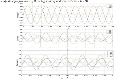
V.A.1 Steady state performance of three leg split capacitor based DSTATCOM
Fig. 3: Steady state performance of split capacitor based DSTATCOM before compensation - a) Source voltages (Vsabc), b) source currents (isabc) and source neutral current (isn) before compensation, c) load currents (ilabc) and load
Fig 3(a) shows the three phase source voltages of 400 V L-L (rms), 50 Hz. Fig 3(b) shows the distorted three phase source currents before compensation. This distortion in source currents is due to usage of linear unbalanced load and non-linear load. Due to the unbalance in the source currents there exists a source neutral current. Fig 3(c) shows the distortion in the load currents due to the usage of linear unbalanced load and non-linear load.
Fig. 4: Steady state performance of split capacitor based DSTATCOM after compensation - a) Source voltages (Vsabc), b) source currents (isabc) and source neutral current (isn) after compensation, c) filter currents (ifabc)
Fig. 5: DC link voltage (Vdc) across the dc link capacitors in split capacitor based DSTATCOM - a) Dc link voltage
across the first capacitor (Vdc1), b) dc link voltage across the second capacitor (Vdc2), c) zoomed view of voltage
unbalance across the two split capacitors (Vdc1 + Vdc2)
With the help of PI controllers the voltages (Vdc1, Vdc2) is nearly maintained at 520 V. The main drawback of this
topology is the voltage unbalancing issue. The voltage unbalance is shown in Fig 5(c). This voltage will cause more stress across the VSI switches which in turn leads to a lack in the performance of the system.
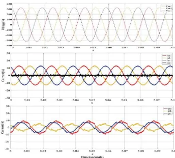
V.A.2 Steady state performance of three leg single dc link capacitor based DSTATCOM
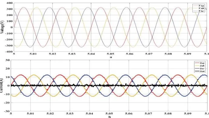
Fig. 6: Steady state performance of single dc link capacitor based DSTATCOM - a) Source voltages (Vsabc), b) source
currents (isabc) and source neutral current (isn) after compensation, c) filter currents (ifabc)
Fig 6(b) shows the three phase source currents (isa, isb, isc) after the compensation provided by the split capacitor based
DSTATCOM. In order to bring the source currents as balanced sinusoidal one, the compensator currents or filter currents shown in Fig 4(c) are injected into the line by means of an interfacing inductor. Source currents after compensation has equal magnitude and proper phase displacement between each other. At the same time the source neutral current (isn) also nearly limited to zero.
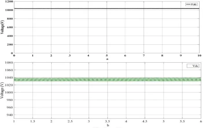
Fig. 7: DC link voltage (Vdc) across the dc link capacitor in single dc link capacitor based DSTATCOM - a) DC link
voltage (Vdc) across dc link capacitor (Cdc), b) Zoomed view of dc link voltage across dc link capacitor
With the help of PI controller, the voltage across dc link capacitor (Vdc) is maintained at 1040 V. Since this topology
uses only a single dc link capacitor, the voltage unbalancing issue associated with the split capacitor based DSTATCOM topology is eliminated here.
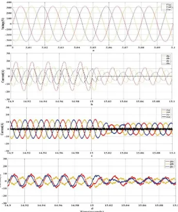
V.B Dynamic performance comparison of both the DSTATCOM topologies.
Fig. 8: Dynamic performance of split capacitor based DSTATCOM - a) source voltages (Vsabc), b) load currents (ilabc)
and load neutral current (iln), c) source currents (isabc) and source neutral current (isn) after compensation, d) filter
currents (ifabc)
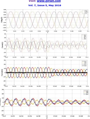
Fig. 9: Dynamic performance of single dc link capacitor based DSTATCOM - a) source voltages (Vsabc), b) load
currents (ilabc) and load neutral current (iln), c) source currents (isabc) and source neutral current (isn) after compensation,
d) filter currents (ifabc)
In this topology also, the DSTATCOM provides the compensator currents into the line and makes the source currents as balanced one. The load changes from full load to half load after t = 15 seconds. It is shown in Fig 9(b).
Table II: Time taken to settle after the occurance of fault
Topologies Settling time after the clearance of fault (seconds) Split capacitor based DSTATCOM 0.04
Single DC link capacitor based DSTATCOM 0.01
Table II shows the split capacitor based DSTATCOM takes 0.04 second to clear the fault. But, in case of single dc link capacitor based DSTATCOM it takes only 0.01 second to clear the fault. This shows that single dc link capacitor based DSTATCOM has faster response than the split capacitor based DSTATCOM.
Table III: Simulation results: Fundamental currents value and THD (%) of source currents (isabc)
Source currents (isabc)
Split capacitor based DSTATCOM Single dc link capacitor based DSTATCOM
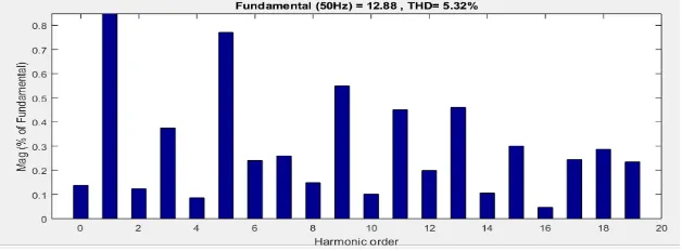
Fundamental current value THD Fundamental current value THD isa 12.88 5.32 12.65 4.51
isb 12.80 5.40 12.63 4.78
isc 12.84 5.30 12.59 4.39
From the Table III, it is clearly shown that all the source currents (isabc) becomes more or less equal after compensation
in both the topologies. But, Single dc link capacitor based topology is well better than Split capacitor based topology in case of total harmonic distortion. Another important factor is when the load contains more amount of dc component, it will lead to major voltage unbalancing issue across the capacitors.
Fig. 10: Harmonic spectrum of phase ‘a’ in Split capacitor based DSTATCOM
Fig. 11: Harmonic spectrum of phase ‘a’ in Single dc link capacitor based DSTATCOM
observed that the THD level and the amount of dc component is high in split capacitor based DSTATCOM when compared to single dc link capacitor based DSTATCOM. Since the amount of dc component is directly proportional to voltage unbalancing issue, the split capacitor based DSTATCOM having more amount of dc component is affected by more voltage unbalancing issue.
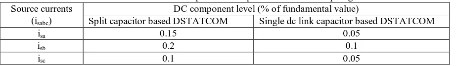
Table IV: DC component level present in both the topologies Source currents
(isabc)
DC component level (% of fundamental value)
Split capacitor based DSTATCOM Single dc link capacitor based DSTATCOM
isa 0.15 0.05
isb 0.2 0.1
isc 0.1 0.05
Table IV shows the amount of dc component present in three- phase source currents. It is clear that split capacitor based DSTATCOM topology has more amount of dc component than single capacitor based DSTATCOM topology. So, it shows that split capacitor topology has more voltage unbalancing issue when compared to single dc link capacitor topology.
VI. CONCLUSION
The performance of the both the topologies for power factor correction, load balancing, harmonic compensation and neutral current compensation are demonstrated through various simulation studies. Split capacitor based DSTATCOM topology has a serious problem of voltage unbalance and having more amount of dc component in it. But single dc link capacitor based DSTATCOM has the advantage of no voltage unbalancing issue and having less amount of dc component in source currents and at the same time it can able to eliminate the source neutral current (isn) with the help
of small ac neutral capacitor. So overall single dc link capacitor based DSTATCOM has more advantages and performs well when compared to the split capacitor based DSTATCOM.
REFERENCES
[1] Singh, B., Jeyaprakash, P., Kothari, D.P., Chandra, A., Al Haddad, K., “Comprehensive study of DSTATCOM configurations”, IEEE Trans. Ind. Inf., Vol.10, pp.854-870, 2014
[2] Sreenivasarao, D., Agarwal, P., Das, B.,“Neutral current compensation in three-phase, four-wire systems: a review”, Electr. Power Syst. Res, Vol 86, pp. 170–180, 2012 [3] Iyer, S., Ghosh, A., Joshi, A.,“Inverter topologies for DSTATCOM applications – a simulation study”,Electr. Power Syst. Res, Vol. 75, Issue (2–3), pp. 161–170, 2005 [4] Singh, B., Arya, S.R., Jain, C., Goel, S., “Implementation of four-leg distribution static compensator”, IET Gener. Transm. Distrib, Vol.8, Issue.6, pp. 1127–1139, 2014 [5] Mishra, M.K., Ghosh, A., Joshi, A., Suryawanshi, H.M.,“A novel method of load compensation under unbalanced and distorted voltages”, IEEE Trans. Power Deliv,
Vol.22, Issue.1, pp. 288–295, 2007
[6] Singh, B., Jayaprakash, P., Kothari, D.P.,“Three single phase voltage source converter based three-phase four wire DSTATCOM”, Proc. IEEE Int. Conf. on Power Systems, pp. 1–5, 2009
[7] Karanki, S.B., Geddada, N., Mishra, M.K., Kumar, B.K., “A DSTATCOM topology with reduced DC-link voltage rating for load compensation with nonstiff source’, IEEE Trans. Power Electron., Vol.27, Issue.3, pp. 1201–1211, 2012
[8] Kumar, C., Mishra, M.K., “An improved hybrid DSTATCOM topology to compensate reactive and nonlinear loads”, IEEE Trans. Ind. Electron, Vol.61, Issue. 12, pp. 6517–6527, 2014
[9] Mishra, M.K., Joshi, A., Ghosh, A., “Control schemes for equalization of capacitor voltages in neutral clamped shunt compensator”, IEEE Trans. Power Deliv, 2003,Vol.18, Issue. 2, pp. 538–544, 2003
[10] Shukla, A., Ghosh, A., Joshi, A.,“Control schemes for DC capacitor voltages equalization in diode-clamped multilevel inverter-based DSTATCOM”, IEEE Trans. Power Deliv, Vol.23, Issue. 2, pp. 1139–1149, 2008
[11] Srikanthan, S., Mishra, M.K.,“DC capacitor voltage equalization in neutral clamped inverters for DSTATCOM application”, IEEE Trans. Ind. Electron., Vol. 57, Issue. 8, pp. 2768–2775, 2010
[12] Chen, Y., Mwinyiwiwa, B., Wolanski, Z., Ooi, B.T., “Regulating and equalizing DC capacitance voltages in multilevel STATCOM”, IEEE Tran. Power Deliv, Vol. 12, Issue. 2, pp. 901–907, 1997
[13] ManjathuValappilManojKumar.,Mahesh Kumar Mishra., “Three-leg inverter-based distribution static compensator topology for compensating unbalanced and non-linear loads” IET Power Electronics., Vol.8, Issue. 11, pp. 2076-2084, 2015
[14] Ghosh, A., Joshi, A.,“A new approach to load balancing and power factor correction in power distribution system”, IEEE Trans. Power Deliv, Vol.15, Issue. 1, pp. 417– 422, 2000