Three Stage Push Pull Inverters Based
Transimpedance Amplifier
Harshit Parmar 1, D.S.Ajnar 2, P.K.Jain 3
P.G. Student (Microelectronics and VLSI Design), Department of E&I, Shri G. S. Institute of Technology and Science Indore, M.P, India 1
Associate Professor (Microelectronics and VLSI Design), Department of E&I, Shri G. S. Institute of Technology and Science Indore, M.P, India 2
Associate Professor (Microelectronics and VLSI Design), Department of E&I, Shri G. S. Institute of Technology and Science Indore, M.P, India3
ABSTRACT: In this paper, a transimpedance amplifier is designed using 0.18μm CMOS technology. In the proposed
transimpedance amplifier (TIA), feedback resistor Rf of conventional transimpedance amplifier which was
implemented using PMOS transistor has been replaced by NMOS transistor as an active feedback resistor. This circuit
operates at 1.6 V power supply voltage and for a current of 3μA. The proposed transimpedance amplifier posses high gain, low noise, low power dissipation, and high bandwidth. The proposed Transimpedance Amplifier exhibits a power dissipation of 0.871mwatt, transimpedance gain of 54.55 dB, a bandwidth of 371.32MHz, an input-referred noise which is equal to 0.827×10⁻¹²A/√Hz.
KEYWORDS:Transimpedance amplifier, High gain, High Bandwidth, Low noise, Low power dissipation, Push-Pull inverters topology.
I. INTRODUCTION
The most basic definition of a Transimpedance amplifier is, It is a current to voltage converter. It is mainly used to amplify the signal from sensor, such as photodiode. In optical sensing systems, the generated current from photodiodes are generally small and most of the processing’s at later stage occurs in the voltage domain, thus it needs to be converted into voltage.
Hence we can say that there is a wide range of applications where we can use the Transimpedance amplifier, because Optical receivers are used in almost every day to day used things. From a house-hold used Television to High speed Optical communication system, optical receivers are used. Every Optical Receiver will use a photodiode to convert the photons into current. To convert this incoming current to voltage, Transimpedance amplifier is used. Hence Transimpedance amplifier is a widely used device.
II. RELATED WORK
The topology used in Reference [1] is Differential Regulated cascode topology which works on the process technology
of 0.18μm CMOS technology. It was mainly designed for optical interconnects. But differential regulated cascade topology results in more noise, hence [2] comes up with another topology named as 1 stage push-pull inverter based transimpedance amplifier. It was mainly for an integrated CMOS optical receiver with clock and data recovery circuit.
It works on the process technology of 0.35μm CMOS technology. Here the noise produced is less as compared to [1].
[3] uses a regulated cascade input stage with shunt feedback topology. Here the supply voltage is 3V. This paper presents the design of an optical receiver analog front-end circuit capable of operating at 2.5 GHz. Fabricated in a
low-cost 0.35μm digital CMOS process, this integrated circuit integrates both transimpedance amplifier and post limiting amplifier on a single chip. Shunt-shunt feedback topology with cascade gain stage is proposed in [4]. The cascode topology is used to reduce the input capacitance of the amplifier and increase the bandwidth. . The amplifier has been designed to be pseudo differential in order to improve the common mode rejection. The optical front end presented in [5] will have application in Optical Scanning Acoustic Microscope System (O-SAM), which involves a totally non-contact method of acquiring images of the interaction between surface acoustic waves (SAWs) and a solid material to be characterized. In this work, an ultra fast optical front-end using improved regulated cascade scheme is developed based on AMS 0.35mm CMOS technology. The receiver consists of an integrated photodiode, a transimpedance amplifier, a mixer, an IF amplifier and an output buffer. Five stage push-pull inverter based topology is proposed in [6]. This paper presents an integrated optical receiver which consists of an integrated photodetector, and a transimpedance circuit. A series inductive peaking is used for enhancing the bandwidth. The proposed structure operates at a data rate of 10 Gb/s with a BER of 10-20 and was implemented in a 0.35 μm CMOS process. CMOS Regulated cascade with inverter based Cherry Hooper amplifier was designed in [7]. It was a 1.57mwatt CMOS Transimpedance Amplifier for VHF Micromechanical Reference Oscillators. In [8] three stage push-pull inverters based topology is introduced which was optimized for detecting very weak signals generated for microscopy imaging in the scanning electron microscope (SEM).
III.CIRCUIT DESIGN
The three stage push-pull inverters based Transimpedance amplifier is shown in fig.2. It consists of three inverters connected with each other serially. Also after every inverter a NMOS with diode connected load is placed which is used to increase bandwidth and decrease miller effect. In proposed TIA circuit, a feedback resistor was also used which is replaced with NMOS transistor as an active feedback resistor biased by the gate voltage Vbias. Besides better controllability, the implementation of the feedback resistor using a NMOS saves chip area immensely. The value of feedback resistor can be determined by using equation 1, which is as follows-
Rf = L eq. (1)
WμCox(Vgs-Vt)
where W =width, L = length, Vgs = gate to source voltage, Vt = threshold voltage and μCox= Transconductance
There is a voltage source Vdd of 1.6 V which is applied to each PMOS transistor. Amplification of signal occurs from input to output. In TIA output is taken at terminal Vout, and a portion of output is given as feedback to the input of the amplifier.
The Gain of the Transimpedance amplifier is given by the ratio of the output voltage to the input current.
A = Vout eq. (2)
Iin
Fig.2.Circuit diagram Of Proposed Transimpedance amplifier.
Three stages transimpedance amplifier consist of three identical cascaded stages having seven NMOS transistor and
three PMOS transistor. A photocurrent of 3μA is used in the circuit. A dc voltage of 1.3 V is applied to the feedback
transistor as a biasing voltage. The transistors should be in saturation region in order to make them work as amplifier, except the feedback transistor which works in linear region because it is to be used as a resistor.
IV.SIMULATION RESULTS
The simulation is carried out using Spectre simulator of Cadence . The simulator works on 0.18μm CMOS technology. Gain Calculation of TIA: As explained earlier, the gain of a Transimpedance amplifier is given by the ratio of the output voltage to input current. The gain of single stage TIA is given by,
A= gm13+gm20 eq.(3)
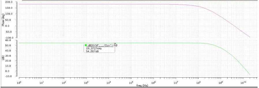
In order to calculate the gain of three stage TIA, the cube of single stage TIA is done. This is because the stages of TIA are connected in series, hence the gains of all the stages are multiplied. Since the aspect ratios of all the stages are same, hence the gain of all the stages will remain same and the overall gain will be cube of single stage TIA. The gain thus calculated is 54.55 dB. Fig 3 shows the gain of proposed TIA.
Fig. 3. Gain of Proposed TIA
Bandwidth calculation of TIA: The 3 dB bandwidth of the TIA is calculated at the point where the gain drops by 3dB. The bandwidth enhancement is one of the most important factor in designing a TIA. The bandwidth enhancement is done by proper selecting the value of the diode connected MOS. Mathematically the bandwidth can be calculated by a formula-
Bandwidth = 1+A eq.(4)
2ΠRfC
Where A is the gain, Rf is the feedback resistance and C is the capacitance. The bandwidth thus calculated is obtained
as 371.32MHz. Fig 4 shows the bandwidth of proposed TIA.
Fig. 4. Bandwidth of Proposed TIA
sources (By open circuiting the current sources and short circuiting the voltage sources), this noise thus calculated will not show the effect of the input sources on the device, Hence In this noise calculation the current source is placed in the circuit and then the noise is calculated. The noise thus calculated is obtained as 0.827×10⁻¹²A/√Hz. Fig 5 shows the noise of proposed TIA.
The power dissipation of the device should be as low as possible. Here the DC Power dissipated is 0.871mW.
Fig. 5. Noise of Proposed TIA
Layout of Proposed TIA: After the analysis and calculations are done, The layout of the proposed TIA is made by the layout tool “Asshura” of cadence. The connections are done in such a manner so that their should not be any Design rule Check (DRC) error. Fig 6 shows the layout of proposed TIA.
TABLE I
PERFORMANCE COMPARISON OF THIS WORK WITH RECENTLY PUBLISHED TIA’S
V. CONCLUSION
A transimpedance amplifier is designed using 0.18μm CMOS technology. In the proposed transimpedance amplifier
(TIA), feedback resistor Rf of conventional transimpedance amplifier which was implemented using PMOStransistor has been replaced by NMOS transistor as an active feedback resistor. This circuit operates at 1.6V power supply
voltage and for a current of 3μA. The proposed transimpedance amplifier posses low noise, low power dissipation, high
gain and high bandwidth. The simulation results shows that the proposed Transimpedance Amplifier exhibits a power dissipation of 0.871 mW, transimpedance gain of 54.55 dB, bandwidth of 371.32 MHz, an input referred noise of 0.827×10⁻¹²A/√Hz. Table I shows the comparison of various topologies of TIA’s with this work. The future work in this amplifier can be done in terms of increasing the number of stages and to decrease the sizing of the transistors. Here the minimum length is taken as 180nm. With the advancement of Technology, the length and width of the device will decrease and thus the power dissipation will also decrease.
REFERENCES
[1] S. M. Park, J. Lee, and H.-J. Yoo, “1-Gb/s 80-dBΩ fully differential CMOS transimpedance amplifier in multichip on oxide technology for optical interconnects,” IEEE J. Solid-State Circuits, vol. 39, no. 6, pp. 971–974, Jun. 2004.
[2] Y.-J. Chen, “An integrated CMOS optical receiver with clock and data recovery circuit,” M.Eng. thesis, Dept. Faculty Eng., Built Environ. Inf. Technol., Univ. Pretoria, Pretoria, South Africa, 2005.
[3] W.-Z. Chen and C.-H. Lu, “Design and anaylsis of a 2.5-Gbps optical receiver analog front-end in a 0.35-μm digital CMOS technology,” IEEE Trans. Circuits Syst. I, Reg. Papers, vol. 53, no. 5, pp. 977–983, May 2006.
[4] R. D. Bespalko, “Transimpedance amplifier design using 0.18 μm CMOS technology,” M.S. thesis, Dept. Elect. Comput. Eng., Queen’s Univ., Kingston, ON, Canada, 2007.
[5] M. Li, “5 GHz optical front end in 0.35 μm CMOS,” Ph.D. dissertation, Dept. Elect. Electron. Eng., Univ. Nottingham, Nottingham, U.K., 2007.
[6] H. Escid, M. Attari, M. A. Idir, and W. Mechti, “0.35 μm CMOS optical sensor for an integrated transimpedance circuit,” Int. J. Smart ens. Intell. Syst., vol. 4, no. 3, pp. 467–481, 2011.
[7] M.-H. Li, C.-S. Li, L.-J. Hou, Y.-C. Liu, and S.-S. Li, “A 1.57mW 99dBΩ CMOS transimpedance amplifier for VHF micromechanical reference oscillators,” in Proc. IEEE Int. Symp. Circuits Syst., May 2012, pp. 209–212.
[8] Joon Huang Chuah and David Holburn, “Design of Low-Noise High-Gain CMOS Transimpedance Amplifier for Intelligent Sensing of Secondary Electrons,” IEEE J. Sensors, vol. 15, no. 10, Oct. 2015.
[9] J. Hu, Y.-B. Kim, and J. Ayers, “A low power 100M_ CMOS frontend transimpedance amplifier for biosensing applications,” in Proc. 53rd IEEE Int. Midwest Symp. Circuits Syst., Aug. 2010, pp. 541–544.
Design of TIA [1] [2] [3] [4] [5] [6] [7] [8] This work
Process Technology 0.25μm Si CMOS 0.35μm Si CMOS 0.35μm Si CMOS 0.18μm Si CMOS 0.35μm Si CMOS 0.35μm Si CMOS 0.18μm Si CMOS 0.35μm Si CMOS 0.18μm Si CMOS Topology Differential Regulated Cascode 1-stage push pull inverter Regulated cascade input with shunt feedback Shunt-shunt feedback with cascode gain stage Improved regulated cascode 5-stage push pull inverters Regulated cascode with Cherry-Hooper amplifier 3-stage push pull inverters 3-stage push pull inverters Supply
voltage(volt) 2.5 3.3 3 3.5 3.3 3.3 1.5 3.3 1.6
Bandwidth 670MHz 910.5MHz 2.2GHz 1.8GHz 6GHz 10Gb/s 280MHz 12.5MHz 371.32MHz
Input referred
noise(pA/√Hz) 20.9 6.03 17.1 9 21 25.8 - 3.54 0.827
Power
consumption 27mW - - 115mW - 87.4mW 1.57mW 60mW 0.871mW
[10] V. A. Lalithambika, “Application of VLSI to optical wireless networks,” Ph.D. dissertation, Dept. Eng., Univ. Cambridge, Cambridge, U.K., 2002.
[11] M.-S. Park, C.-S. Shim, and M.-H. Kang, “Analysis of sensitivity degradation caused by the flicker noise of GaAs-MESFETs in fiber optic receivers,” J. Lightw. Technol., vol. 6, no. 5, pp. 660–667, May 1988.