ISSN(Online): 2319-8753 ISSN (Print): 2347-6710
I
nternational
J
ournal of
I
nnovative
R
esearch in
S
cience,
E
ngineering and
T
echnology
(An ISO 3297: 2007 Certified Organization)
Website: www.ijirset.com Vol. 6, Issue 5, May 2017
Design and Simulation Analysis of Power
Factor Correction Using Boost Converter with
IC UC3854
Santhosh Kumar R
1, Shreeshayana R
2Assistant Professor, Department of EEE, ATMECE, Mysuru, Karnataka, India1 Assistant Professor, Department of EEE, ATMECE, Mysuru, Karnataka, India 2
ABSTRACT: In recent scenario many appliances requires DC power supply. Hence to obtain the DC power from input ac supply, Power Electronics circuits like Rectifiers which is a non-linear load has to be used. The current drawn by these non-linear load will be phase will not follow the supply voltage (i.e non sinusoidal). This results in a High Total Harmonic Distortion (THD) and Low Power Factor (PF). Hence the Power factor has to be improved and line current harmonics has to be reduced. The most commonly used topology for improving the PF in supply side is Active PFC using boost converter. The design and simulation of boost converter with Average Current Mode control in continuous conduction mode is presented in this paper. The output waveforms of the Power Factor Correction circuit is compared using two simulation tools.
KEYWORDS : Average Current Mode Control, Active Power Factor Correction, Continuous Conduction Mode.
I. INTRODUCTION
The demand on solid state AC-DC power converters increases from time to time. They are employed in several application areas such as uninterruptable power supplies (UPSs), back up energy storage systems, hybrid electric vehicle chargers, power supply for telecom loads and adjustable speed drives (ASDs). However, the power converters draw pulsating input current from the utility grids which results in poor power factor. Meanwhile, the converters pollute the AC mains by injecting significant amount of harmonic current from the switching devices due to high switching frequency. Improving the poor power quality becomes a great challenge for power supplying utilities as well as power converter manufacturers. The PFC circuit can reduce a significant amount of current harmonics. Low electromagnetic interference (EMI) can be achieved by employing boost type PFC converter as compared to other types of active PFC converters in continuous conduction mode (CCM). Moreover, most of the bridgeless topologies implemented so far are boost type configuration (also referred as dual-boost PFC rectifiers) because of its low cost and its high performance in terms of efficiency, power factor and simplicity. Hence, this project targets to design power factor correction using boost converter [1].
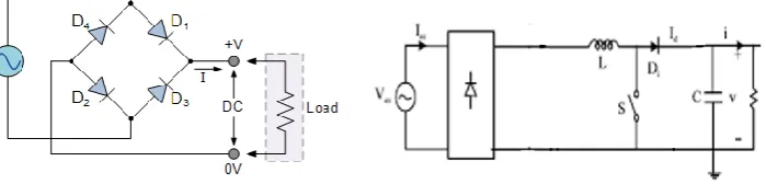
The input ac supply is converted into dc using diode bridge rectifier with a large output filter capacitor is cheap and robust, but it demands a harmonic rich ac line current. The rectification circuit as shown in Fig. 1, where the input power factor is poor. The low power factor and high pulsating current from the AC mains are the main disadvantages of the diode rectifier. Rectification is used in SMPS. So, power factor of SMPS is very poor.
ISSN(Online): 2319-8753 ISSN (Print): 2347-6710
I
nternational
J
ournal of
I
nnovative
R
esearch in
S
cience,
E
ngineering and
T
echnology
(An ISO 3297: 2007 Certified Organization)
Website: www.ijirset.com Vol. 6, Issue 5, May 2017
To overcome these type of power quality problems different power electronics converter topologies are employed, out of which the boost converter topology has been extensively used as shown in Fig. 2. The boost converter can be operated in two modes, namely continuous conduction mode (CCM) and Discontinuous conduction mode (DCM). Any on method can be used for the PFC. In this paper we present the CCM of operation.
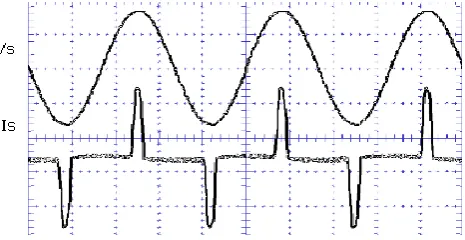
In the boost converter the capacitor maintains a voltage of approximately the peak voltage of the input sine wave until the next peak comes along to recharge it. In this case, current is drawn from the input only at the peaks of the input waveform, and this pulse of current must contain enough energy to sustain the load until the next peak. It does this by dumping a large charge into the capacitor during a short time, after which the capacitor slowly discharges the energy into the load until the cycle repeats. The input current waveform that doesn’t follow the input voltage waveform is as shown in Fig. 3.
Fig. 3. Supply Current and Voltage Waveform without PFC
There are two control objectives for the boost converter in a PFC, namely Attaining a nearly constant output voltage and Keeping the average value of the input current nearly proportional to the input voltage thus obtaining a close to unity power factor.Fig.4 shows Power Factor Correction Using Boost Converter andFig.5 shows the waveform of the supply current and voltage after the PFC circuit.
Fig. 4. Power Factor Correction Using Boost Converter Fig. 5. Supply Current and Voltage Waveform with PFC
ISSN(Online): 2319-8753 ISSN (Print): 2347-6710
I
nternational
J
ournal of
I
nnovative
R
esearch in
S
cience,
E
ngineering and
T
echnology
(An ISO 3297: 2007 Certified Organization)
Website: www.ijirset.com Vol. 6, Issue 5, May 2017
II. RELATEDWORK
[2] Presents a bridgeless AC DC boost converter operating in CCM. The implementation of input current and output voltage controller is also discussed. Then a comparative analysis based on simulation results of bridgeless and bridge boost rectifier is presented. Bridgeless boost AC-DC converter has outperformed the conventional techniques due to lower conduction losses, lower THD of input current and improved input power factor.
[3] Introduces a single-stage active power factor correction (PFC) AC-DC converter which provides almost unity power factor and minimizes the THD to 7.4 %. For a constant DC output voltage a single phase diode bridge rectifier with a large output capacitor is considered in this paper. This standard topology has a shortcoming of introducing lower order harmonics and become cause of poor power factor, which needs to be improved.
[4] deals with an active input power factor correction with single phase bridge rectifier fed boost converter topology using hysteresis current control technique. The duty ratio is obtained by the comparison of a inductor current and a ramp carrier waveform which is associated with hysteresis controller in each switching period. Improvement in the supply current is illustrated in this work.
[5] In this paper, a novel discrete model has been proposed to simulate the controller IC UC3854. The main contributions are as followings: 1)The power stage of the Boost converter has been modelled by using the large signal approach and the loop gain of current program has been put forward; 2) The continues-time voltage control diagram has been investigated by employing equivalent power stage which contains the main circuit and current program; 3) Based on the continues-time model, a new discrete model of PFC has been given out and the operational principle has been introduced; 4) A 4kw prototype has been built up to verify the validity of the new model; Results of the simulation and the experiment show that the power factor is 96.7%.
[6] Presents an advanced Average Current-Mode Control (ACMC) technique for single phase AC-DC Boost Converter with Reactive Power Control. The leading phase admittance cancellation (LPAC) principle has been proposed to eliminate the current phase lead phenomenon. It results in reduction of the current control loop bandwidth requirement for a given line frequency.
III.AVERAGE CURRENT MODE CONTROL
The boost topology is a popular choice for a single-phase ac-dc pre-regulator with high power factor and low harmonic distortion of line ac current. The recently proposed ACMC has been widely used in PFC application.
ISSN(Online): 2319-8753 ISSN (Print): 2347-6710
I
nternational
J
ournal of
I
nnovative
R
esearch in
S
cience,
E
ngineering and
T
echnology
(An ISO 3297: 2007 Certified Organization)
Website: www.ijirset.com Vol. 6, Issue 5, May 2017
IV.SYSTEM MODELLING
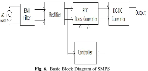
Power supply is the device that transfers electric power from a source to a load using electronic circuits. A typical application of power supplies is to convert utility’s AC input power into regulated DC voltage required for electronic equipment. Depending on the mode of operation of power semiconductors PSU can be linear or switching (SMPS). The basic block diagram of SMPS is as shown in Fig. 6.
Fig. 6. Basic Block Diagram of SMPS
The SMPS mainly consist of EMI Filter section to attenuate the high frequency electromagnetic signals, Rectifier to convert AC to DC and then the reregulated Power Factor Correction circuit to improve the Power factor by reducing the THD levels. Finally it has DC-DC converter to get the desired output voltage.
The paper presents a design for the PFC circuit using Boost converter in closed loop mode to get the stable output voltage and to improve Power factor and hence efficiency. Then hardware model is done to verify the output of the designed circuit.
Another objective is to design a EMI filter which should pass only the line frequency signal and attenuate all other high frequency electromagnetic signals.
V. PFCCONTROL CIRCUIT DESIGN
The operating requirements for the active power factor corrector is Pout (max): 240W, Vin range: 80-270Vac,Line frequency range: 47-65Hz,Output voltage: 400Vdc,Select switching frequency: 100 KHz.
A. Passive Component Design
Inductor value is found using following steps
(min) pk
* 2 I
n in
i V
P
________________________(Eqn.1)
= 1.41 x240/80=4.23 A
Ripple current
ΔI=0.2 * Ipk
ISSN(Online): 2319-8753 ISSN (Print): 2347-6710
I
nternational
J
ournal of
I
nnovative
R
esearch in
S
cience,
E
ngineering and
T
echnology
(An ISO 3297: 2007 Certified Organization)
Website: www.ijirset.com Vol. 6, Issue 5, May 2017
The duty factor at
________________________(Eqn.2)
D= (393-280)/393 D= 0.287
L= (280x0.287)/(100,000x0.846) = 0.949mH Let L=1.0 mH
Output Capacitor value is found using following steps
2 V 2 V Δt * P * 2 C 1 0 out 0 __________________________(Eqn.3)
Where is the hold-up time in seconds and 𝑉1 is the minimum output capacitor voltage.
= 2.3mF.
Let C0 = 1mF.
Total peak current
________________________(Eqn.4)
B. Control Circuit Design:
Sense Resistor value.
_____________________(Eqn.5)
Choose RS = 0.25 Ω
Peak sense voltage
___________________(Eqn.6) =4.653*0.25 0 in(Peak) 0 V V V D
t
2 ΔI I Ipk(max) pkA 4.653 2
0.846 4.23
Ipk(max)
pk(max) rs S I V R 0.21Ω 4.653 1 RS
s pk(max) rs(peak)
I
*
R
V
ISSN(Online): 2319-8753 ISSN (Print): 2347-6710
I
nternational
J
ournal of
I
nnovative
R
esearch in
S
cience,
E
ngineering and
T
echnology
(An ISO 3297: 2007 Certified Organization)
Website: www.ijirset.com Vol. 6, Issue 5, May 2017
Resistors in voltage divider
Assume peak current overload value
Vrs(vold)Ipk(vold)*RS
____________________(Eqn.7)
= 5.6*0.25 =1.4V 1.87K 5 . 7 10000 * 4 . 1 R pk2
Maximum peak voltage
637k
6 -10 * 600 V R peak(max) vac
Choosing RVAC=620KΩ Bias resistor
R 0.25*R 155KΩ vac
b1
Choosing Rb1= 150kΩ
Sense resistor 10KΩ I * 2 3.75 R ac(min)
set
1.25nF 100K * 10K 1.25 f * R 1.25 C S set
t
VI.CIRCUIT SIMULATION AND RESULTS
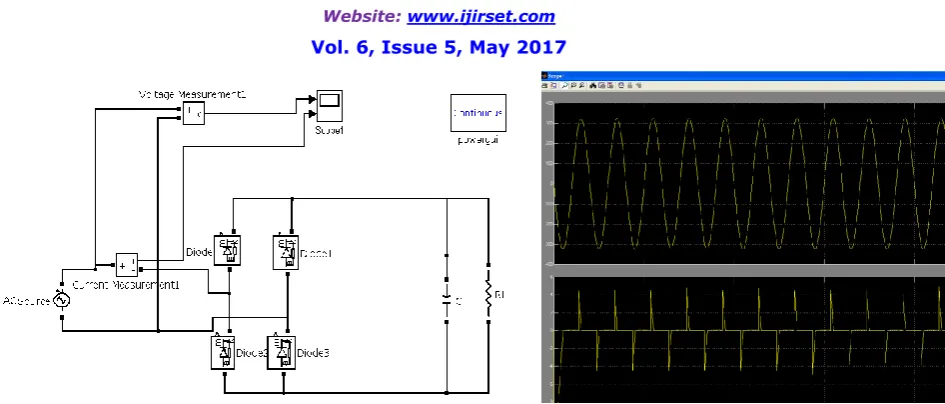
Circuit simulation is carried out using MATLAB Simulink and PSIM simulation softwares. The circuit was simulated without APFC circuit and with APFC circuit for rectifier. Circuit simulation of rectifier without Active PFC Circuit is shown in Fig. 7
382V V
* 2
ISSN(Online): 2319-8753 ISSN (Print): 2347-6710
I
nternational
J
ournal of
I
nnovative
R
esearch in
S
cience,
E
ngineering and
T
echnology
(An ISO 3297: 2007 Certified Organization)
Website: www.ijirset.com Vol. 6, Issue 5, May 2017
Fig .7. Simulated Rectifier Circuit without PFC Circuit Using MATlab Fig .8. Simulated Waveform of Rectifier Circuit Without PFC Circuit Using MATlab
From the simulated result shown in Fig 8, We can observe that the input current waveform shape is not same as that of input voltage and hence the power factor is going to reduce. The input power factor in this case will be around 0.4 to 0.6.
Circuit simulation of Rectifier with Active PFC Circuit is shown in Fig. 9. From the Simulated Waveform Of Rectifier Circuit With PFC Circuit Using MATlab is shown in Fig.10 which shows improvement in power factor i.e 99%.The current and voltage waveform can be seen in the Fig.10 and the test results are tabulated to verify the circuit designed.
Fig .9. Simulated Rectifier Circuit With PFC Circuit Using MATlab Fig .10. Simulated Waveform of Rectifier Circuit with PFC Circuit Using MATlab
ISSN(Online): 2319-8753 ISSN (Print): 2347-6710
I
nternational
J
ournal of
I
nnovative
R
esearch in
S
cience,
E
ngineering and
T
echnology
(An ISO 3297: 2007 Certified Organization)
Website: www.ijirset.com Vol. 6, Issue 5, May 2017
TABLEI:SIMULATED RESULT WITH PFC
Input
Voltage(V)
Input
Current(A)
Output
Voltage(V)
Power factor
200 4 400 0.99
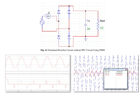
The Simulation of Rectifier circuit without PFC using PSIM simulation software is shown in Fig.11.The parameters designed and implemented in simulink, were also applied here. The results of the current and voltage waveforms have been discussed in the sections below.
Fig .11 Simulated Rectifier Circuit without PFC Circuit Using PSIM
Fig .12. Output Current and Voltage Waveform without APFC
ISSN(Online): 2319-8753 ISSN (Print): 2347-6710
I
nternational
J
ournal of
I
nnovative
R
esearch in
S
cience,
E
ngineering and
T
echnology
(An ISO 3297: 2007 Certified Organization)
Website: www.ijirset.com Vol. 6, Issue 5, May 2017
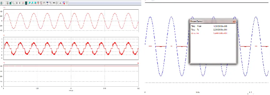
Fig .13. Circuit Diagram of PFC Using IC UC3854 (Analog Technique)
Fig .14. Simulation Result with PFC
From the Fig.14 we observe that the current waveform in phase with the voltage waveform and the power factor is improved i.e to 98%. The result is tabulated in Table 2 below which shows almost similar results obtained with simulink software. The analysis was performed to test the efficiency of the designed circuit.
TABLE2:Simulated result with PFC
Input
Voltage(V)
Input
Current(A)
Output
Voltage(V)
Power factor
200 4 400 0.986
VII. CONCLUSION
The implementation of Average Current Mode Control (ACMC) with Boost converter using analog circuits (i.e. employing feedback using Voltage amplifier and Current amplifier) provided appreciable power factor. The power factor can be improved to about 98% by using this technique.
ISSN(Online): 2319-8753 ISSN (Print): 2347-6710
I
nternational
J
ournal of
I
nnovative
R
esearch in
S
cience,
E
ngineering and
T
echnology
(An ISO 3297: 2007 Certified Organization)
Website: www.ijirset.com Vol. 6, Issue 5, May 2017
caused by the rectified circuit can be nullified by Active Power Factor Correction circuits implementing Average current mode control with Boost converter using analog circuits.
REFERENCES
[1] M. H. Rashid, Power Electronics Handbook, New York: Academic Press, 2001.
[2] Mukhzan Mobeen Ali, Sardar Shazali Sikander, Usman Ali and Arbab Waleed, “An Active Power Factor Correction Technique for Bridgeless Boost AC-DC Converter”, IEEE Explore, ISBN: 978-1-4673-8752-1, pp.129-134, 2016.
[3] Pratap Ranjan Mohanty, Anup Kumar Panda and Dhiman Das, “An Active PFC Boost Converter Topology for Power Factor Correction”, IEEE India Conference, ISBN: 978-1-4673-7399-9, pp.1-5, 2015.
[4] S.Ramprasath, P.Ramesh Babu andA.Rekha, “Design and Simulation of Superior Quality Input Current Rectifier Based on Boost Topology” International Conference on Circuit, Power and Computing Technologies, ISBN: 978-1-4799-7075-9, pp.1-5, 2015.
[5] R. Weiping Zhang, Fei Chen , Xusen Zhao and Yuanchao Liu, “A Discrete Modelling for Power Factor Correction Circuit”, IEEE Explore, pp.160 – 163, 2010.
[6] Parag Karekar, Ankit Deshpande, “Average Current-Mode Control with Leading Phase Admittance Cancellation Principle for Boost Converter”,International Journal of Emerging Research in Management &Technology, Vol. 4,Issue 5, 2015