ABSTRACT
TSHIBANGU, NYUNYI MARCUS. Study and Analysis of Energy-Efficient DRAM-Cache with Unconventional Row-Buffer Size. (Under the direction of Dr. Paul Franzon).
The development of 3DIC technology has given rise to a new generation of fast and
dense memories. These memories consist of multiple cell layers stacked on top of each other
using interconnect in both X, Y, and Z dimensions. The vertical interconnect in this
Die-stacking technology can help reduce the size, increase the speed, and reduce the energy
simultaneously. These advantages have given researchers the motivation to incorporate the
stacked DRAM as last level cache (LLC) or DRAM-cache. It is the goal of architects to have
a fast and large memory on-chip, but the current SRAM cache technology provides a
limitation. Therefore, a DRAM-cache is an alternative to achieving both high density, speed,
and proximity to CPU. Studies to date demonstrating this used a 2KB row size and up. If the
industry adopts a widespread use of DRAM for cache, stacked DRAMs need organization
suitable not only for better performance but also for energy efficiency. In this work, we have
studied and analyzed a range of DRAM cache with row buffer size ranging from 256B to 4
KB, and we determined that a DRAM cache mapped in unconventional 512B row buffer
stacked memory is a better choice. Such stacked DRAM was set up to provide two independent
ports with access to 32 independent banks each. A smaller row size significantly cut off the
energy per access at row buffer miss. An 8-way single-set single-row and energy-efficient
mapping (SSSR-LE-8) configuration achieved 36, 40, and 74 % improvement in overall energy
consumption compared to 3 other configurations mapped in 2KB row buffer memory. This
low-energy mapping at the same time also increased the performance by 16, 18, and 41%. The
simulator was modified to account for variable hit latency due to row buffer hit status. The
© Copyright 2016 by Nyunyi Marcus Tshibangu
Study and Analysis of Energy-Efficient DRAM-Cache with Unconventional Row-Buffer Size
by
Nyunyi Marcus Tshibangu
A dissertation submitted to the Graduate Faculty of North Carolina State University
in partial fulfillment of the requirements for the degree of
Doctor of Philosophy
Electrical Engineering
Raleigh, North Carolina
2016
APPROVED BY:
_______________________________ ______________________________ Dr. Eric Rotenberg Dr. W. Rhett Davis
________________________________ ________________________________ Dr. Bryan Floyd Dr. Gregory Buckner
________________________________ Dr. Paul Franzon
DEDICATION
To my Father, Karl Mukeba, Thank you for inspiring me to pursue higher education during
your short and precious journey here on Earth. I owe you this degree.
BIOGRAPHY
Nyunyi Marcus Tshibangu was born in the city of Mbuji-Mayi, Democratic Republic of
Congo, as the last of eight children. Four years after he graduated from high school, he moved
to the US in 2002 to pursue high education. In 2006 he graduated from the University of North
Carolina at Charlotte (UNCC) with a degree in Electrical Engineering. Upon graduation, he
joined the Timken Corporation as Control’s engineer providing support in Automation for high
volume manufacturing of package bearings from 2006 to 2009. Earlier 2008, he joined NC
State University to pursue his Masters in Electrical Engineering with a focus on Electronic
Circuit and System (ECS). Upon completion of Masters at the end of 2009, he joined ESAB
Corporation as R&D Hardware and Software Engineer for the development of electronic
control system used for the design and fabrication of automatic welding and cutting machines,
based on plasma, oxy-fuel and laser technology.
In spring 2012, He came back to NC State to continue with his PhD in Electrical and
Computer Engineering. Given his industrial exposure to control system, he planned to join the
control and mechatronics research area but this quickly changed when in summer of 2012, he
was offered an important role in “3D implementation of Heterogeneous processor”, a project
sponsored by Intel Corporation under the direction of Dr. Paul Franzon. This completely
changed his research interest to memory system and computer architecture. Being a big
proponent of “learning by doing”, he joined a low-power CPU group at Intel Corporation for
ACKNOWLEDGMENTS
First I would like to Thank God for his gift of salvation and countless blessings in my life.
From a little boy born in the heart of Africa to finishing a PhD and playing important roles in
the American society, I do not take anything for granted. From putting me in contact with the
greatest and supportive wife (Priscas Mbaya) and having an amazing daughter (Kalubi
Tshibangu) and son (Nyunyi M. Tshibangu), as well as my unborn child, he set me for success
as the support and motivation they are giving me is unprecedented and I am forever grateful.
Second, I would like to thank my Father (Karl Mukeba) and my Mother (Celine
Mpunga) for their amazing love and support. They gave me a deep understanding of the
importance of education and my whole life I have done everything in my power to reach the
highest level of education possible and make them proud. To all my brothers and Sisters, in
the US and abroad, thank you for your love and support and this degree is my way of loudly
express that.
Finally, I would like to thank Dr. Paul Franzon first, for endorsing my admission in the
ECE department and second for accepting to take me as his student and providing me with
guidance, constructive criticism, financial and technical support to complete my work. He
allowed me to overstay my journey at Intel Corporation and gain additional industrial
experience and a huge opportunity to advance my career with the company. To Dr. Davis and
Dr. Rotenberg for allowing me to become part of this great IntelH3 project and providing
feedback that has contributed to my success. In particular, Dr. Rotenberg for igniting my
interest in computer architecture and for his comprehensive and detailed feedback that
conversations beyond academic. To Dr. Floyd and Buckner thank you for serving on my
TABLE OF CONTENTS
LIST OF TABLES ... ix
LIST OF FIGURES ...x
CHAPTER 1 – Introduction ...1
1.1. Motivation and Objectives ...1
1.2. Overview of Chapters ...2
CHAPTER 2 – Memory System in Modern Computers ...5
2.1. Memory Technology and Classification ...5
2.2. Random Access Memories ...7
2.2.1. SRAM ...8
2.2.1. DRAM...9
2.3. Computer Performance ...12
2.4. Memory Hierarchy Overview ...16
2.5. Cache Organization ...19
2.6. Cache Performance Optimization ...21
2.6.1. Reducing Miss Rate ...21
2.6.2. Reducing Miss Penalty ...23
CHAPTER 3 – Three-Dimensional Integrated Circuits (3DIC) ...24
3.1. Motivation ...24
3.2. Advantages ...27
3.3. 3DIC Integration Process ...28
3.3.1. TSV ...31
3.3.2. 3D vs 2.5D ...31
3.3.3. Die-Stacked DRAM ...35
3.4. Thermal Challenges in 3DIC ...37
CHAPTER 4 – State-of-arts in Stacked Memory Applications...39
4.1. Overview ...39
4.2. Tag mapped in DRAM...41
4.2.1. Single Set Single Row High Associative (SSSR-HA) ...41
4.2.2. Multiple Set Single Row Direct map (MSSR-DM) ...46
4.2.3. Multiple Set Single Row Set Associative (MSSR-SA) ...49
4.2.4. Multiple Set Single Row Set Associative with 4K row buffer ...51
4.2.4.1. MSSR-8S-7 ...51
4.2.4.2. MSSR-2S-29 ...51
4.3. Tag-in-SRAM consideration ...54
4.3.1. Tag Cache ...54
4.3.2. Hybrid SRAM/DRAM Cache ...55
4.4. Page-based cache ...57
CHAPTER 5 – Energy-Efficient DRAM-Cache with Unconventional Row-Buffer ...60
5.1. Overview ...60
5.2. Low Energy Stacked DRAM consideration ...61
5.3. Low Energy Configuration Mapping ...65
5.3.1. Single Set Single Row 16-way configuration (SSSR-16)...66
5.3.2. 8-way Single Set Single Row Low Energy Configuration (SSSR-LE-8) ...69
5.4. Rationale for Small size Row buffer leading to Low Energy-efficient Config. ...71
5.4.1. Scenario 1: DRAM Cache Hit ...72
5.4.2. Scenario 2: DRAM Cache Miss ...72
5.5. Estimation of Hit latency and Energy per access ...74
5.5.1. Estimation Equations ...74
5.5.2. Assumption used for latency and Energy parameters ...75
5.5.3. Latency and Energy per access ...77
5.5.4. Pros and Cons of Alloy-cache (TAD) ...78
5.5.5. Additional advantages of our low-energy configuration SSSR-LE-8 ...79
CHAPTER 6 – Simulation and Results ...81
6.1. Assumptions ...81
6.2. Methodology ...82
6.2.1. Workloads ...82
6.2.2. Simulator Setup ...83
6.3. Results and Analysis ...87
6.3.1. Figure of Merit: Execution time & DRAM Cache energy ...87
6.3.2. Other Metrics ...92
6.3.2.1. Miss Rate ...92
6.3.2.2. Row Buffer Hit Rate ...95
6.4. Improvement from SRAM LLC ...98
6.5. Summary ...100
CHAPTER 7 – Survey of Stacked DRAM specs for low-energy DRAM Cache ...101
7.1. Overview ...101
7.2. Methodology ...102
7.3. Impact of Row buffer Size on performance ...105
7.3.1. Row Buffer size of 256B ...105
7.3.2. Row Buffer size of 512B ...107
7.3.3. Row Buffer size of 1KB ...110
7.3.4. Row Buffer size of 2KB ...113
7.3.5. Row Buffer size of 4KB ...115
7.3.6. Pareto Optimality for a choice of energy-efficient Stacked DRAM organization...116
7.3.7. SRAM Consideration ...119
CHAPTER 8 – Case Study: Design of Controller for a shared Last Level DRAM Cache
Mapped in Tezzaron 3D stack Memory...124
8.1.Overview ...124
8.2. Tezzaron Memory specs ...125
8.3. Micro-architecture...126
8.4. DRAM Cache Controller ...129
8.4.1. Read Datapath ...130
8.4.2. Write Datapath ...131
8.4.2. Controller ...132
8.5. Preload: A 3D specific possibility ...134
8.5.1. Motivation ...134
8.5.2. Case Study: Rationale of Pre-load ...136
8.6. Design Consideration from Octopus2 to DiRAM4 ...138
8.6.1. Difficulty of converting to DiRAM4 ...138
8.6.2. DiRAM4 Read and Write constraints ...141
CHAPTER 9 – Conclusions and Future Work ...142
9.1. Conclusion ...142
9.2. Future Work: Heterogeneity ...143
BIBLIOGRAPHY ...144
APPENDICES ...152
Appendix A – Simulator Tutorial ...153
A.1. GEM5 Installation ...153
A.2. GEM5 Execution ...154
A.3. Change made to GEM5 ...155
A.3.1. Bank/row/port extraction logic per configuration ...155
A.3.2. Code modification ...157
Appendix B – DRAM Cache Controller based on Tezzaron DiRAM4 ...167
B.1. Introduction ...167
B.2. RTL code ...169
LIST OF TABLES
Table 5.1. Timing and Energy parameters of 2KB vs 0.5 KB row buffer stacked memory ...64
Table 5.2. Summary of Total DRAM Size, 3Ts, and 3Es ...76
Table 5.3. Summary of DRAM cache Hit latency and Energy per access ...77
Table 6.1. Workload Simulated ...82
Table 6.2. Average performance Summary ...91
Table 7.1: 256MB Stacked DRAM Combinations of specs ...103
Table 7.2. CACTI3DD specs for 256B row buffer memory with 1 port ...105
Table 7.3. CACTI3DD specs for 256B row buffer memory with 2 port ...105
Table 7.4. Comparison of 1-port vs 2-port on 256B row buffer ...106
Table 7.5. CACTI3DD specs for 512B row buffer memory with 1-port ...107
Table 7.6. CACTI3DD specs for 512B row buffer memory with 2-port ...107
Table 7.7. Comparison of 1-port vs 2-port on 512B row buffer ...108
Table 7.8. CACTI3DD specs for 1KB row buffer memory with 1-port ...110
Table 7.9. CACTI3DD specs for 1KB row buffer memory with 2-port ...110
Table 7.10. Comparison of 1-port vs 2-port on 1KB row buffer ...111
Table 7.11. CACTI3DD specs for 2KB row buffer memory with 1-port ...113
Table 7.12. CACTI3DD specs for 2KB row buffer memory with 1-port ...113
Table 7.13. Comparison of 1-port vs 2-port on 2KB row buffer ...114
Table 7.14. CACTI3DD specs for 4KB row buffer memory with 1-port ...115
Table 7.15. Comparison of row buffers from 256B to 4 KB ...116
LIST OF FIGURES
Figure 2.1: Basic SRAM Cell ...8
Figure 2.2. Basic 1T1C DRAM Cell ...10
Figure 2.3. H & P Clock Frequency trend ...13
Figure 2.4. H & P Processor-Memory Gap...14
Figure 2.5. Example of Memory hierarchy ...17
Figure 2.6. 4-way set associative cache ...20
Figure 3.1. ITRS Cross-section of wire scaling ...25
Figure 3.2. ITRS roadmap for copper (Cu) Resistivity ...26
Figure 3.3. 3D stack orientation ...30
Figure 3.4. 3D topology ...33
Figure 3.5. 2.5D topology ...34
Figure 4.1. SSSR-HA: The Loh-Hill configuration ...42
Figure 4.2. Loh-Hill DRAM cache access using MissMap ...44
Figure 4.3. MSSR-DM: The alloy-cache ...47
Figure 4.4: Memory Access Predictor (MAP) ...48
Figure 4.5. Hameed et al MSSR-SA configuration based on 2KB row buffer ...50
Figure 4.6. Hameed et al MSSR-8S-7 configuration based on 4KB row buffer ...52
Figure 4.7. Hameed et al MSSR-2S-29 configuration based on 4KB row buffer ...53
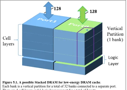
Figure 5.1. A possible Stacked DRAM for low energy DRAM cache ...62
Figure 5.2. Ports/banks/Rows organizations ...63
Figure 5.3. 16-way Single Set Single Row low-energy configuration (SSSR-16) ...68
Figure 5.4. 8-way Single Set Single Row configuration (SSSR-LE-8) ...70
Figure 5.5. DRAM cache hit vs. RBH/RBM ...72
Figure 5.6. DRAM cache miss vs. RBH/RBM ...73
Figure 6.1. Total Energy per run ...88
Figure 6.2. Total Execution Time per run...90
Figure 6.3. Detailed Miss Rate per run ...93
Figure 6.4. Average Miss Rate ...94
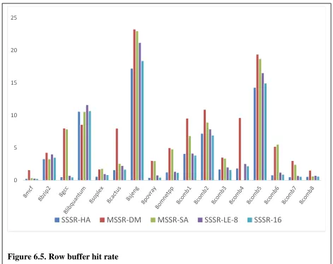
Figure 6.5. Row buffer hit rate...96
Figure 6.6. Average Row Buffer Hit Rate (RBHR)...97
Figure 6.7. Total Execution Time per run for SRAM LLC ...99
Figure 6.8. Detailed Miss Rate per run for SRAM LLC ...99
Figure 7.1. Possible configurations from 512B 2-port row buffer memory ...109
Figure 7.2. Possible configurations from 1 KB 2-port row buffer memory ...111
Figure 7.3. Figure 7.3. Pareto Optimality: Energy vs hit time ...118
Figure 7.4. Total execution time for variable configurations within 512B row buffer ...121
Figure 7.5. Total Energy for variable configurations within 512B row buffer ...122
Figure 7.6. Average Miss Rate (AMR) for variable configs within 512B row buffer ...123
Figure 7.7. Average Row Buffer Hiss Rate (ARBHR) within 512B row buffer configs ...123
Figure 8.1. Tezzaron Octopus2 Bank specs ...125
Figure 8.2. Tezzaron Octopus2 Timing specs ...126
Figure 8.3. Micro-architecture based on Sparc T2 [29] ...128
Figure 8.5. DRAM Cache Controller Read Datapath ...130
Figure 8.6. DRAM Cache Controller Write data path ...131
Figure 8.7. Controller ...133
Figure 8.8. DRAM Cache Controller based on Tezzaron DiRAM4 specs ...140
CHAPTER 1
INTRODUCTION
1.1.
Motivation and Objectives
3DIC allows the design of fast and high-density memory. It gives research opportunity to study
the utilization of DRAM for the on-chip cache. The high-density memories built on vertical
stacks can solve the size limitation of SRAM technology. The vertical interconnect can help
reduce the size, increase speed and bandwidth, and reduce energy per access. This research
work investigates the implementation of such stacked DRAM into low-energy and
high-performance last-level cache or DRAM-cache for multicore processors. Recently, few studies
have been conducted to use stacked DRAM as last level cache. There are two motivations for
this. First, these 3DIC DRAM allows I/O busses as large as 128-bit which increases bandwidth
compared to regular DDR DRAM with only 16-bit in data transfer. Second, the large size
compared to any last level cache in modern processors can offset the average access latency
by significantly reducing capacity miss.
In these recent studies, the focus is put mostly on performance for obvious reasons, but
very few studies focus on performance while optimizing energy consumption in these DRAM
caches. In this work, we will put our focus on energy consumption while keeping a competitive
level of return in term of CPU execution time. Even though 3DIC technology can reduce the
energy per access on DRAM, the total number of accesses and the size of data can significantly
make a difference in the overall energy consumption. Most recent studies have simply
a large row of 4KB [7], and an extra-large row of 8KB [24]. In this research, we are studying
the implementation of DRAM-cache configuration using unconventional row size optimized
for better energy consumption
and increased performance. To do this, we cannot just be limited to large pages used in
traditional DDR memories. In contrast, we are proposing the utilization of stacked memory
with a small page. The primary motivation to this is the fact that a smaller row size reduces the
energy per access during row operation such as the activation and precharge. This energy
reduction is also noticed at read and write when a row is already open.
1.2.
Overview of chapters
Before we get into our main research objectives, we took the time to gather all the necessary
information that can make our study accessible and understandable by a vast majority of
readers, not just the experts in the field. Therefore, we are giving a good overview of memory
technology and hierarchy, computer performance, 3DIC technology and its challenges. Below
is an outline of each chapter.
Chapter 2 is an overview of memory technologies used in industry today and their
applications in computer design and performance. We put an emphasis on memory hierarchy
using these type of memories. Since our research is in large part studying cache, it is in our
best interest to mention cache organization and optimization as implemented in traditional
Chapter 3 is a general overview of Three-dimensional Integrated circuits (3DIC).
Because it is a focus of this dissertation, it is suitable to dedicate time in literature to review
the implementation of this technology. We are focusing on advantages and disadvantages of
this technology including the most known challenges such as thermal issues that have slowed
down the widespread implementation in commercial products.
Chapter 4 is the state-of-arts literature on stacked DRAM applications on which we
have based our study and motivations. We are summarizing several proposed configurations
and analyzing their advantages and disadvantages that have led to our recommended
configurations and methodology for improvement.
Chapter 5 is the central part of our dissertation that focuses on our proposal and detailed
study of its implementation. We have studied and analyzed a baseline configuration suitable
to reach our objective of energy saving and demonstrate the advantages of using a stacked
DRAM with a smaller page.
Chapter 6 lays out the simulation and methodology used to test our proposed
configurations as well as a comparison to configurations mapped in larger row buffer memory.
We have used CACTI3DD [40] to estimate the energy and timing model for all settings, and
we described our modification made to GEM5 [41] simulator to extract CPU time and power
numbers that are 3D specifics. This simulator originally evaluates cache hierarchy designed in
2D SRAM technology. Using stacked DRAM for cache requires implementation of its
In chapter 7 we conducted a survey of different row buffer sizes to complete our study
of low-energy DRAM cache. The goal is to find a better organization of DRAM for
energy-efficient last level of cache.
Chapter 8 focuses on our tape-out that led to the fabrication of DRAM-cache controller
chip to control Tezzaron DiRAM4 3D stacked memory. This study includes the controller
architecture, micro-architecture, pre-silicon design, and validation. It also describes many
challenges encountered as well as solution needed for the success of the project. Chapter 9 is
our concluding remark and future work.
We also added a comprehensive appendix section to give a reader a better
understanding of our methodology and a possibility to duplicate work and results. In Appendix
A, we provide in detail changes that were made to the simulator and in Appendix B, a copy of
CHAPTER 2
Memory System in Modern Computers
2.1. Memory Technologies and Classifications
This section defines the different classification of memory and their impacts in modern
computers. The demand in computer performance requires a lot of memories at both core and
system-level. At the core level, more than half the transistors are dedicated to memory in the
form of cache [8]. Particularly it is the case at system-level where off-chip memory is needed
to keep up with computation bandwidth requirement. Therefore, different memory types are
required to fit the system requirement in cost, density, and speed.
There are three main classifications of semiconductor memory: read-only memories
(ROM) also characterized as non-volatile, read-write memories (RWM) also called volatile,
and Non-volatile Read-write memories (NVM). The data in ROM is hard-wired and can only
be read but not written, and its integrity does not depend on the existence of power source.
Most use of these types of memories in modern computers is for firmware or initialization of
information during system boot-up. On the other side, RWM can both be read and written
during the process and requires the continuous existence of power source to keep the integrity
of data.
The most popular type of RWM is Random Access Memory (RAM) and its two
variants: SRAM and DRAM (static/dynamic Random access memories). Random refers to
their abilities to read and write data in any order. It is a contrast to serial memories where the
An example of these is FIFO (first-in-first-out) and LIFO (last-in-first-out) which used
for stacks and queues. The two characteristics that make a major different in RAM are "static”
and “dynamic”. Static refers to its ability to retain data with continuous power source only.
While in dynamic, the existence of permanent power supply is not enough. To maintain data
integrity, periodic read and write operations are required. It is known as refresh.
The third and most emerging class of memories is the non-volatile read-write memories
(NVM). Among these are EPROM (Erasable Programmable), EEPROM (Electrically Erasable
Programmable), and FLASH memories. The latter is the fastest growing type of memories that
serve to design mass storage as a better alternative to magnetic disks used for hard-drive.
Solid-State-Drive (SSD) uses NAND flash memory as main storage unit [80] [81]. The storage cell
used in almost all NVM is the floating-gate transistor which is an MOS device with an extra
polysilicon stripe floating between the gate and channel hence the name floating-gate. The high
voltage across the drain-source injects hot electron able to cross the first oxide and get trapped
in the floating gate and changes the property of threshold voltage. This state corresponds to
logic 1. Because the floating gate is insulated between a thick silicon oxide, charges can remain
even after the removal of the power supply. Hence the name non-volatile.
Not all non-volatile memories use floating-gate as a storage device. Some use the
magnetic property to store data instead of electrical property as used in MOS devices. An
example of such memories is Magneto-resistive RAM (MRAM) or Spin-Transfer Torque
RAM (STT-RAM). The storage device in MRAM is the magnetic tunnel junction (MTJ) which
consists of two ferromagnetic layers whose directions determine the data stored. Recently,
energy and simplifies the design. But because it is still at an earlier stage, their 64Mbit density
does not meet the current memory demand.
2.2. Random-Access Memories
Because we are studying the application of DRAM for cache purpose, it is important to
elaborate more on these types of memories. RAM, as mentioned above, allows the system to
read and write in random orders. The two kinds classified in this category depends on the
storage methods. When data is stored in a latch, its value remains as long as the power is active
and this type of storage or cell is called static and give rise to static RAM (SRAM). However,
when data is stored in a capacitor, its value can change as the capacitor discharges with time
and this type of storage or cell is called dynamic RAM (DRAM). SRAM is often a preferable
on-chip memory for its speed, data integrity and mostly fabrication technology that is
compatible with CMOS logic. But its limited density due to a large and costly cell size has led
to consideration of DRAM for on-chip application. The widespread use of DRAM for on-chip
applications is through embedded DRAM or e-DRAM [37] [38], and most recently the DRAM
cache mapped in 3D memory is being studied for its ability to integrate logic chip and storage
2.2.1. SRAM
SRAM cell consists of two back-to-back inverters forming a latch to preserve the integrity of
data as shown in Figure 2.1. This basic CMOS device consists of six transistors. Four are used
in the two inverters that form a latch, and the other two important NMOS are pass transistors
used for read or write operations. The word line (WL), used as enable bit, activates these pass
transistors. The bit lines value of BL= 0 and conversely BL_N = 1 writes a zero to the cell. If
the cell were previously high, its value would change to low. The contrast is applied when
writing the value 1. Since this device requires at least six transistors, SRAM density is low,
and its cost per bit is high.
The 6T back-to-back inverter SRAM cell shown here is the most basic device to keep density
few improvements have been proposed regarding additional transistors. These complex cells
can hold 7, 8, 9 and even 10 transistors [74] [75] [76]. The drawback of increased transistor
count is the increase in cost and area. So some improvements are being made on the 6T to
increase stability [77] and keep small area and low cost for mass production.
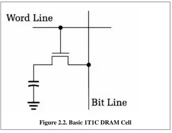
2.2.2. DRAM
A DRAM cell consists of a single transistor and a capacitor known as 1T1C cell as shown in
figure 2.2. The transistor is used to charge and discharge a capacitor during a write or read
operation. For a write operation, while the word line is raised high, the bit line value of 1
charges the capacitor, and the value of 0 discharges it. For a read operation, the bit line (BL)
capacitor is pre-charged to a certain voltage (typically Vdd/2) before the WL is activated.
When WL is high, the charges are redistributed between the two capacitors and there is a
change in voltage on BL that determines the value of the cell. The sense amplifiers detect this
voltage change and store the resultant value in built-in registers or cache called row buffer. At
every read or write to the same column, data is accessed from the buffers rather than bit-cell
itself. The reason for this is because during the read operation, the modification of cell charge
So instead of restoring the data right after read, most DRAM controllers wait until a
different row access is required before writing back data stored in row buffers. It is called
open-page policy as opposed to the closed-open-page policy, typically not frequent. Because data is stored
in a capacitor, not only it is lost after a read operation and power source removal, but also when
the capacitor discharges through leakage over time. Therefore, a periodic refresh is required to
keep the integrity of data. This refresh is simply a row activation (ACT) followed by a write
back of data from row buffer before row closing (PRE) (e.g. REF = ACT + PRE). Most
memory controllers keep track of the discharge time with internal counters. Typically,
depending on temperature, an interval of 8 ms to 64 ms is required to refresh active rows of
the DRAM. Because the cell size is small, the density of a DRAM is high and the cost per bit
is much lower compared to SRAM. Millions of these bit cells can be organized into an array
of rows and column called banks.
A single DRAM chip can content many independent banks (e.g. 16) controlled by
separate circuits (e.g. decoders, sense amps, drivers, buffers). The bank address selects a bank,
and once active, the row address selects the row to activate. This operation is called row access
strobe or RAS. During RAS operation, the word lines (WL) of a group of cells are driven high.
The column address selects the group of bit lines to read or write. This operation is typically
called column access strobe or CAS. Because of bandwidth requirement, column read or write
is done in a consecutive range of address called burst mode, often locating 2, 4, or 8 different
column addresses on a single CAS. To reduce access time, this is done on both rising and
falling edge of the clock or double data rate (DDR). Even though 1T1C cell is the most popular
and most economically sound, there are still some variations of this. A 2T1C cell consisting of
an extra transistor [78] [79] had been proposed for embedded DRAM applications. This cell is
called gain cell and is claimed to be logic compatible. But because DRAM is always being
designed for low leakage and low cost, 1T1C still the most favorite bit cell for most
2.3. Computer Performance
From 1986 until 2003, the frequency of CPU was increasing by 40% per year (e.g. 16.7
MHZ to 3.2 GHZ) as shown in figure 2.3 [9] and the Processor performance regarding memory
requests per second also increased by 52% per year as shown in figure 2.4 [9]. But in the same
period, the memory performance has been less than 7 % per year showing an increasing gap
between the processor and DRAM. In the last decade, this aggressive improvement in CPU
has seen a tremendous slow-down as the frequency increase and performance improvement
has flattened out down to less than 1% per year [9]. This analysis shows that the CPU of a
single processor has reached the maximum frequency that does not provide a noticeable
increase in performance. Twenty years ago this was predicted through the idea of memory wall
[12]. This idea states that as the off-chip memory access time diverges significantly from cache
access time, the average memory access time will grow and therefore degrading the
performance. As the speed of the memory determines the overall system performance, it has
Figure 2.3. [9]. H & P Clock Frequency trend.
Figure 2.4. [9]. H & P Processor-Memory Gap.
Another reason for flat frequency is the dependency of power and energy consumption
on switching speed of transistors. As feature size decreases, the number of transistors that can
fit on a single chip dramatically increases and dominates the power equation (fcv²) despite a drop in voltage (v) and transistor capacitance (c). So continuing to increase frequency in a
single processor has led to a power wall [9]. Because of the memory and power walls, modern techniques to optimize performance has focused on studying simultaneous computation by
exploring different parallelism within a single processor: Instruction-level parallelism (ILP),
and data-level parallelism (DLP) or through multiprocessors: Thread-level parallelism(TLP).
These parallelism techniques are designed to hide memory latencies and reduce processor stalls
giving a virtual ladder to climb over the wall [14]. Even though there is a noticeable
performance improvement due to these multiple advancements in CPU computation
techniques, there is also a net energy consumption increase due to their logic and hardware
complexity. Therefore, a continuous research to improve memory hierarchy is required to
break this persistent memory wall entirely and hopefully, reduce energy consumption while
2.4. Memory Hierarchy Overview
Traditionally, the memory system is designed to exploit the principles of spatial and
temporal locality to reduce the length of the wall. By dividing it into different levels, a
reduction of hit penalty can be achieved. Every increasing level (closer to CPU) is smaller and
faster than its lower counterpart. But unfortunately these fast levels are more expensive as the
cost per byte is a function of size and technology. Inside the CPU are found Register files or a
set of flip-flops to contain data directly needed for computation and logic.
This level of memory (Level 0) is only a few hundreds of bytes (e.g. 500 bytes) and
only within few hundreds of picosecond delay (e.g. 500 ps). The first on-chip two to three
levels are implemented in SRAM. Level-1 cache (L1) is the closest structure to the CPU
register file with a size of tens of kB (e.g. 32kB) and access speed of fewer than two cycles.
Level-2 cache (L2) is relatively large within hundreds of KB (e.g. 256 kB) and access speed
around ten cycles. Level-3 cache (L3) has a size in the magnitude of few MB (e.g. 4MB) and
access speed around 20 cycles. Some systems have a fourth level L4 of on-chip memory, but
On system-level, there is the main memory which is an off-chip DRAM and contains
most of the size of the entire memory hierarchy in GB level (e.g. 8 GB) and access speed
between 50 to 100 ns. Because of its volatility, main memory or any other lower-level
memories cannot store data outside program execution at the absence of power supply.
Therefore, program files and other critical information need to be saved in permanent storage.
There are two types of mass storage today. The first and the oldest is the hard drive (HDD)
which uses a spinning magnetic metal plate to Read and write data. Because of moving
mechanical part, the read/write latency is in order of ms. The second mass storage which is a
potential replacement to HDD is the solid-state drive (SSD) that uses NAND flash memory as
a storage unit. Because of lack of moving parts, SSD is faster and more reliable than HDD. Its
high cost per gigabit (e.g. 4x) still prevents it from replacing HDD but with new Intel
Corporation Micron Technology joint effort on 3D NAND technology [82], eventually, the
cost will go down, and HDD may become as ancient as a floppy drive. Figure 2.5 gives a good
visual representation of the current memory hierarchy for high-end computer processors.
This hierarchy is a way to provide the CPU with fast and close memory for its fast
operation, but unfortunately, the closest and fastest memory is the smallest. Ideally, it is the
goal of architects to have an infinite amount of memory closer to CPU and providing data at
the CPU bandwidth. The continuous research in memory technology is to find the next
generation of disruptive technology that can combine memory and storage in a single level of
hierarchy. Intel Corporation and Micron Technology in their joint effort announced a new
disruptive technology called 3D XPoint [87]. This technology, as they claimed will give rise
2.5. Cache Organizations
Cache is a small size memory organized into small blocks grouped into rows or sets. A typical block size is 16, 32 or 64B. Each block is larger than the operands size and is identified
by its address in the memory. A tag is a portion of this address that identifies the block location
in the memory. The number of blocks into a set determines the associativity or ways. An associativity of one is called direct mapping. Otherwise, it’s a set-associative. On the other extreme, if all the blocks in the cache belong to a single set, it’s referred to as fully associative. The following are the basic cache equations:
𝑏𝑙𝑜𝑐𝑘𝑜𝑓𝑓𝑠𝑒𝑡 = 𝑙𝑜𝑔2(𝑏𝑙𝑜𝑐𝑘𝑠𝑖𝑧𝑒) (2.1) #𝑠𝑒𝑡 = 𝑐𝑎𝑐ℎ𝑒𝑠𝑖𝑧𝑒
𝑎𝑠𝑠𝑜𝑐𝑖𝑎𝑡𝑖𝑣𝑖𝑡𝑦 𝑋 𝑏𝑙𝑜𝑐𝑘𝑠𝑖𝑧𝑒 (2.2) 𝑖𝑛𝑑𝑒𝑥 = 𝑙𝑜𝑔2(#𝑠𝑒𝑡) (2.3) #𝑡𝑎𝑔 𝑏𝑖𝑡𝑠 = #𝑎𝑑𝑑𝑟 𝑏𝑖𝑡𝑠 − 𝑖𝑛𝑑𝑒𝑥 − 𝑏𝑙𝑜𝑐𝑘 𝑜𝑓𝑓𝑠𝑒𝑡 (2.4)
When CPU requests data for computation, the level1 cache controller looks up its
address in tag area. If there is a match, it’s referred to as cache hit and data will be sent to CPU. Otherwise, it’s a cache miss, and the request is redirected to next level in the hierarchy all the way to the main memory. The address is decoded using the above cache equations to calculate
the size of each field. For example, from Figure 2.5, a 32 KB cache with a 64 B block and
4-way associative will be mapped to 128 sets. It will need 7-bit row decoder as the index; 6-bit
2.6. Cache Performance Optimizations
There are three factors used to determine cache performance: hit time, miss rate, and miss
latency. All optimizations techniques used today are targeting a reduction of one or all these
performance metrics. Hit time is the time it takes to access data when it is present in the cache.
It is a function of configuration, circuit design, and technology. Miss rate is the ratio of the
number of access misses to the total number of accesses. It is a function of cache configuration
and program characteristic (e.g. memory intensive will have high miss rate). Miss latency is
the time it takes to get data from next level of hierarchy into the cache after a miss. It is also a
function of cache configuration and circuit optimization.
2.6.1. Reducing Miss Rate
Before talking about miss rate reduction, it’s good to define different types of misses.
Compulsory miss is the first reference to a memory block. A capacity miss occurs as the result of cache capacity or size and does not depend on cache configuration unlike conflict miss that depends on the number of blocks in a set (e.g. associativity). Conflict miss does not exist in a
fully-associative cache. Few techniques are used to reduce miss rate. First, it can be
accomplished by an increase in associativity, block size, or cache size. But there is a limitation
beyond which there is a diminishing return. For instance, when increasing block size, spatial
locality helps to bring neighboring data but beyond a certain threshold, data become polluted
and increase miss penalty. Increasing block size reduces compulsory misses but can also
worsen the other two type of misses in a small cache. Set associative cache has better miss rate
advantage over a 4-way associative of the same size but can dissipate much more energy and
even increase hit latency. Therefore, in most cases, a 4-way associative cache is almost
equivalent to having better miss performance than an extra-large set associative cache of the
same size. Also, an increase in cache size reduces capacity misses but can increase hit penalty
and chip area (e.g. high cost) and power. Therefore, to keep hit time down, smaller caches are
a choice.
Second, prefetching can be used either in hardware or software. The purpose of prefetching is to predict which memory blocks may be needed and get them before the
processor needs them. In hardware, additional logic block and registers are required to
supplement cache. Prefetched instructions or data can be saved into cache or stream buffers.
On a miss, the requested block is fetched and placed in the cache, and the next block is also
fetched and placed in the stream buffer. So on the next demand, the stream buffer is checked
for a match first before a request is sent to next level. In software prefetching, before the
processor misses, software or compiler predicts the access and compute the address of an
instruction and sends a request. Because the processor is not in immediate need of the
instruction, a miss will not stall its execution. For such a miss, the controller can proceed in a
way to overlap with normal execution. Like other techniques used above, prefetching can also
cause cache pollution, meaning fetching useless data and possibly replacing the good ones,
2.6.2. Reducing Miss Penalty
Additional cache level can be added to reduce miss penalty. It does two things. First, it
keeps small cache closer to the processor to keep up with its speed. Second, it holds large
caches in a low-level of hierarchy (e.g. L2, L3) to increase on-chip memory and avoid off-chip
accesses. For instance, IBM Power 7 processor contains three levels of cache with 32MB last
level in embedded DRAM [17]. With this large L3 cache, an implementation in SRAM
technology would have required large area and cost. We will study in more depth throughout
this document the advantage of large caches. Also adding write buffers can allow the CPU to
continue normal execution while write operations are pending. It is understandable that write
misses to level 2 cache do not contribute to overall miss penalty because write backs should
not stall the CPU activities as this can be done in the background while executing other
instructions. However, reads misses to L2 on the other side, whether they are part of load or
CHAPTER 3
Three-Dimensional Integrated Circuits (3DIC)
3.1. Motivation
Integrated circuits (IC) are designed to keep up with Moore’s law which predicted that every
two years, the number of transistors will double [13]. Ever since the transistor size have been
scaled down to reach high performance and low cost. But it is not without consequences. First,
as the device size decrease to low sub-micro scale (e.g. 65,32,22,14 nm), the wire decreases in
cross-section and becomes a very critical elements affecting not only the speed of the circuits
but also the energy dissipation, power distribution, and reliability. The wire introduces
different parasitics (resistive, capacitive, and inductive) which can be modeled as a lump or
distributed elements. Equation 3.1 can estimate the propagation delay when considering only
resistive and capacitive parasitics.
𝑡
𝑝= 0.38𝑅𝐶 = 0.38𝑟𝑐𝑙
2(3.1)
Where R, C are respectively total distributed resistance and capacitance and r and c are
respectively per unit length resistance and capacitance. So R=r*l and C=c*l. The square
relationship of length justifies the rapidly increasing total propagation delay at next technology
node. Global and semi-global wires mostly dominate this increase. In contrast, delays at metal
1 and intermediate wires have little influence as their lengths are usually also scaled down
However, at this low-level metallization, the capacitance is dominant due to congestion and
low pitch wire as shown in Figure 3.1. This growing capacitance also increases power
consumption according to CV^2f relation. At semi-global and global levels, insertion of
repeaters to reduce delay increases area and hence contribute to power consumption increase.
According to ITRS, for process technology less than 22nm, roughness in via sidewall barrier,
and copper surface will all negatively affect electron scattering in copper lines and cause an
increase in resistivity [5]. Figure 3.2 shows that the resistivity of Cu will continue to increase
for deep submicron technology.
Figure 3.1. ITRS Cross-section of wire scaling.
Second, the demand for performance requires more devices to be confined while the
chip increases in size to accommodate for more functionalities. As a result, the total
interconnecting wire also grows in length. These two elements increase the wire resistance and
hence the RC propagation delay. Therefore, a significant portion of power consumption of the
chip is attributed to interconnects [6]. Also, the growing demand for functionality and high
productivity has given rise to system-on-chip (SoC). SoC allows circuits of disparate
technology and mixed-signals such as embedded DRAM, analog, low-power and
high-performance logic blocks to be combined in a single chip. This combination causes numerous
frequency digital circuits. All these challenges mentioned above are the motivations for the
development of three-dimensional integrated circuits or 3DIC [6] [11] [18] [19] [50]. It refers
to vertical interconnection of different circuit blocks into many layers. From equation 3.1,
resistance (R) and capacitance (C) are increasing with technology scaling. The only way to
slow down the growth of delay is to reduce length. As mentioned above, the 2D SoC demand
does not help with this either. So this question can be answered by 3DIC.
3.2. Advantages
3DIC technology has the benefit of reducing global interconnection length. It allows
for the reduction of parasitic and hence reducing energy consumption [49]. The average
reduction of length is by a factor of √𝑁𝑡𝑖𝑒𝑟 [11]. Where 𝑁𝑡𝑖𝑒𝑟represents the total number of layers. Given the linear relationship between power and wire length, the average power
consumption would assume to have the same reduction factor. Because of the vertical stacking,
the increase in volumetric density allows the incremental density of circuit elements (e.g. cell,
MOS devices). It makes it possible to increase the capacity in the same amount of surface area.
This advantage is evident in the design of stacked memories [25] [31] [43] [44]. Many memory
cells can fit in a small area making memory attractive to various architectural innovations. In
this dissertation, we will study the application of stacked DRAMs for cache purpose. We will
explore their advantages over standard 2D memories on bandwidth and energy consumption.
Another advantage of 3DIC is the heterogeneity. It is the co-existence of blocks
fabricated with different technology processes into a single chip. Unlike SoC, these blocks can
between analog and high-performance logic circuits. When designs for various purposes (e.g.
analog/digital/memory) are fabricated separately in their best appropriate technologies, there
is better yield, optimization, and performance for each. Even on a digital portion, 3DIC can
also allow a multicore processor to contain small and large cores [36] which can perform at
different frequencies. It can also integrate cores fabricated in various transistor sizes [48] (e.g.
65 nm and 32 nm) into single chip but different layers.
3.3. 3DIC Integration Process
3DIC has different integration processes. Among these are the vertical interconnect
through bond wires, and the most interesting is the stacking with through-Silicon Via (TSV).
There are four different methods for creating 3DIC chips [50]. Among those methods, there
are chip stacking, transistor stacking, die-on-wafer, and wafer-on-wafer. Chip stacking
refers to connecting standalone chips vertically with wire bonding and flip-chip to reduces the
area overhead. Transistor stacking refers to placing multiple levels of MOS devices on a single substrate. It is the most invasive integration used to contribute to reducing subthreshold leakage
in nano-scale CMOS devices [51] [52]. But the thermal challenges are the main limitations
because any high temperature during process destroys the devices and metals. In die-on-wafer, dies are bonded on top of the un-diced wafer using organic glues or metal bonding. The
interconnect can occur on die edge, face or through silicon. Wafer-on-wafer allows bonding of un-diced wafers through the substrate. Its alignment accuracy is better than die-on-wafer
and reduces cost. Both die-to-wafer and wafer-to-wafer can use direct bonding technology [63]
treatment process to strengthen the bonding between the surfaces. Die-on-wafer and
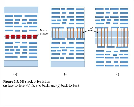
wafer-on-wafer can use through-silicon Via (TSV) for interconnect. There are three different orientations
for stacking: face-to-face, face-to-back, and back-to-back. Face and back are referred
respectively as connecting from the top metal or the substrate (e.g. below metal 1).
The figure 3.3 (a) (b) (c) shows the 3 topologies. Face-to-face is mostly used to connect
logic tiers using metal bonding such as Cu-to-Cu thermo-compression process. Such process
is used by Tezzaron's FaStack [53]. Because this process requires putting chips through harsh
conditions of pressure and high temperature, there are other low-temperature and low-pressure
[55] [56] thermo-compression. There are also non-thermo-compression methods that use room
temperature to produce high-yield throughput [54]. Thermal compression can also apply to
other metal bonding such as Cu-SnAg through a process called self-assembly. This process
uses a high-precision alignment of chip-to-wafer or wafer-to-wafer [61] [62]. Face-to-back
uses TSV to connect logic layers to memory for instance. In back-to-back, TSVs have to go
through two substrates increasing its length and parasitic, therefore making it the least
(a) (b) (c)
Figure 3.3. 3D stack orientation.
3.3.1. TSV
Through-silicon via (TSV) is the interconnect of choice for fabrication of 3DIC chips.
The difference between regular via and TSV is that the former is an inter-metal layer within a
die, but the latter is the pathway between top-metals of separate dies. It is a cylindrical tungsten
or copper filled via that has full electrical characteristics such as resistance, capacitance, and
inductance. These features depend on physical specs and material characteristics such as
length, cross-sectional area and metal conductivity [57] [58]. It is important to study the
electrical characteristics of TSV because they affect the performance of 3DIC. TSV is now
very popular because it helps to reduce the interconnect length in semiconductor chips by
replacing wire bonds and reducing parasitic and noise. Figure 3.3 shows the use of TSVs within
different topologies.
3.3.2. 3D vs. 2.5D
The most known three-dimensional fabrication processes are full 3D stack and 2.5D
using silicon interposer. The former helps connect multiple chips using TSV that pass through
active elements. Whereas the latter only allow TSV to go through a passive platform called
interposer. It means that there are no TSV through the active chips [66]. Both processes avoid
the use of long and slow bond wires that limit interconnect density. Full 3D process relies on
an intensive use of TSV to connect active elements within a die as shown in figure 3.4. It
creates numerous issues including thermal dissipation challenges as described in next section.
Although there is various research in the area of the heat problem, a full production of 3D chips
However, the non-ideal alternative to full 3D but more realistic is the 2.5D process. It
helps avoid the issue created by TSV into active dies. In this process, dies fabricated in different
process and technologies can be glued together on a passive silicon interposer which in turn
serve as connections to package using TSV as shown in figure 3.5. Because all TSVs are on a
passive silicon substrate, the thermal issues can be avoided by applying well know heat
dissipation technics used in standard IC design. Chips are flipped and connected to the
interposer with micro-bumps. The interposer, in turn, is connected to package substrate using
TSV. The most popular type of interposer is the silicon interposer [67] [68]. Recently there
was research conducted on glass interposer that utilizes through-glass vias (TGV) [69]. TGVs
are similar to TSVs, but they are crossing a glass substrate instead of silicon. The motivation
behind this is that glass is an excellent insulator that provides low signal loss. It can increase
3.3.3. Die-Stacked DRAM
Die-stacked DRAMs are a type of memories that combines multiple layers of memory cells
using vertical interconnects. These dense cell layers are fabricated in density-aware DRAM
NMOS processes and sit on top of CMOS logic layer. This bottom layer contains multiple
peripheral circuits such as sense amps, decoders, row buffer cache, drivers, receivers, and
various custom logic and optimization circuits. Unlike 2D DRAM and embedded DRAM [37],
there is a distinct advantage to separate the two technologies for better performance. As logic
layer when designed in CMOS technology, the performance is much higher than when
fabricated in NMOS DRAM process. Conversely, when ato performance-aware CMOS
technology integrates embedded DRAM, there is a loss of density and yield [38].
3D memories with TSVs are more of reality than just research concept. In recent years
few prototypes had been fabricated and tested promising a wide-spread commercial use of 3D
technology soon. In 2010 Samsung published their first fabricated stacked DRAM [25]. It is
11 x 9 mm 8 Gb memory made in 50 nm technology. Each of the four layers represents a
separate rank that consists of 8 banks each. About 300 TSVs with 80 um pitch and measuring
30 um in diameter were used to connect these layers. Their post-silicon results show a reduction
in standby and active power by 50 % and 25% respectively compared to a conventional
quad-die package. In 2011, they also presented a fabricated DRAM that stack two layers of 512 DQs
1Gb wide I/O DRAM for a total of 2 Gb memory [31]. Both micro-bumps and TSVs connect
the 2 RAMs. Each TSV is 7.5 um diameter and about 48 fF of capacitance.
In 2012, Micron published papers for their new stacked DRAM called Hybrid Memory
Cube (HMC) [43] [44]. This 1 Gb memory built on 68 mm2 surface consists of 4 cell layers
contains all peripherals to controls all memory operations. For interlayer interconnect, they
used approximately 1866 TSVs separated by 60um pitch. They approximated its power
consumption at ~10pJ/bit. In 2014, they released a 2GB HMC in a 31 x 31 mm package [85].
Today The Hybrid Memory Cube Consortium (HMCC) is a group of technology leaders
including developers, manufacturers, and earlier adopters who enable HMC technology. Its
goal is to develop a standard protocol for integration of HMC technology into a wide variety
of applications. The latest and recent revision of HMCC specs leverages 18.5 x 22 mm to 34 x
34 mm packages with a density of 4GB and 256 banks to 8GB and 512 banks partitioned
3.4. Thermal Challenges in 3DIC
Despite the many advantages of 3DIC over 2D technology, vertical stacking has its challenges.
3DICs produce high heat density than conventional ICs causing thermal issues due to relative
positions of circuit layers. The thermal problem in 3DIC is a well-researched topic because
heat dissipation is a tremendous challenge for the widespread production of this technology.
Active circuits elements sandwiched within each other prevent heat removal methods from
working efficiently. Even in 2D chip, there is already thermal issues caused by transistor
switching as the frequency increase. But in this case, the heat is conducted to heat sink through
the substrate and dissipated with different cooling methodologies. During 3D stacking, only
one layer is closer to heat-sink leaving other heat dissipating layers far away. Therefore,
elaborate heat removal methods are required to prevent performance reduction in 3DIC, which
can even negate the above-given advantages.
Studies in the recent years have proposed thermal architectures. To reduce the
temperature of the isolated layer and heat-sink layer, Zhang et al. [10] proposed a design
consisting of an air gap and a thermal bridge. They claimed a reduction of temperature from
75 C to 36 C in the memory layer, and down to 60C in processor layer compared to
conventional air-cooling. C. Santos et al. [71] proposed a potential cost-effective thermal
management method by placing graphite-based heat spreaders either on top of exposed stack
or between the stacks. They claimed a temperature reduction down to 45 C. Matsumoto et al.
[72] also proposed the used of graphite-based material in dual-side cooling. The conventional
stack to ensure cooling from the bottom side of the chip. Although many types of research are
CHAPTER 4
State-of-arts in Stacked Memory Applications
4.1. Overview
Few ideas can be explored to use the stacked DRAM efficiently for latency and energy
optimization. There are few ways to utilize a stacked DRAM. A first way is to use it simply as
a traditional main memory but with DRAM stacked on top of processor chip [30] [32] [33]
[34] [35]. A second way is to use it as "on-chip memory" as an extension of off-chip memory
to avoid tagging. It requires the operating system to manage physical address between the two
memory regions. The OS can analyze page usage and determine which ones need to be mapped
in on-chip portion of memory. Remapping pages is not a straightforward operation that
requires software development. Software development can take a substantial amount of time
making this solution a hardware-software issue. The third way is to consider the stacked
DRAM as a shared last level of cache [1] [2] [3] [4] [7] [20] [28]. Some proposed a
combination of SRAM and DRAM cache into a hybrid last level cache to take advantage of
SRAM’s low latency and DRAM’s high capacity [21] [26] [27]. In this scheme, the system
will determine where to place an incoming allocated block.
The first thought is to maintain the separate SRAM for tag [22] [23], but this may
require a large SRAM even bigger than most L3 cache in modern processors. Such a large
SRAM can be slow and power hungry even to the point of negating the speed and energy
saving provided by 3D stacking. Zhao et al. [46] proposed the use of combined on-chip 8-bit
rate. But this works better for small DRAM cache such as 64MB as they used. For large DRAM
cache, this tag overhead will rapidly increase. So the most efficient approach is to map the tag
within the DRAM to eliminate the separate SRAM. In the next section, we will explore
different recent proposals of mapping tag within DRAM and some techniques that can reduce
hit latency and miss rate.
There are recent publications that advocated for the use of large row buffer (4KB or
8KB) for page-based mapping [23] [24]. But we will only analyze in-depth the different
DRAM cache block-based mappings that take advantage of the conventional 2 KB row size
DRAM. With up to 32 blocks in 2 KB row, some authors have used the entire row as a single
set providing an extra-large associativity to take advantage of spatial locality and reduce
conflict miss. Others have mapped multiple sets inside a single row. Amongst those, some have
made every block to represent a set making it direct mapped, but others have separated small
and equal groups of blocks into multiple sets with reduced associativity. Each mapping style
has its advantages and drawbacks as will be analyzed throughout this document. In the next
few sections, we will explore these proposals that target different goal. Miss rate and Hit
latency are the two parameters that all of them are targeting to improve performance. In section
4.2, we explore proposals that map tag in DRAM. Among them, some focus on reducing miss
rate, some on hit latency, and others on both. In section 4.3, we explore proposals that map tag
in SRAM or use both SRAM and DRAM as last level cache. In section 4.4, we will talk about
4.2. Tag mapped in DRAM
4.2.1. Single Set Single Row High Associative (SSSR-HA)
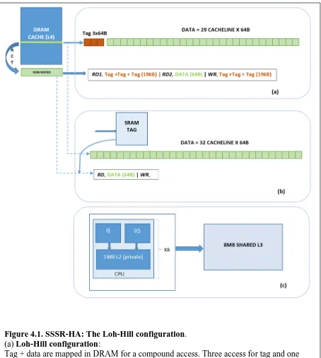
Loh and Hill [1] [2] proposed a tag-in-DRAM cache where three blocks contain tags,
and 29 blocks include data all within a single row as captured in figure 4.1 (b). This compound
mapping avoids opening a new row in case of a hit as row-buffer hit is guaranteed. Each block
consists of 64B for the total page or row of 2KB. The motivation behind this scheme is to avoid
a large external SRAM for tag store as captured in figure 4.1 (a). For instance, a 256MB DRAM
will require about 24MB of tag space which is already larger than last level cache of most
processors. Considering the nature of SRAM, such a large tag structure will create extra
overhead in area and also add additional latency to overall access time. Combining tags and
data within the DRAM eliminates this cost although it reduces the cache capacity (e.g. 232MB
with 24MB dedicated for tags). Therefore in this work, we will consider tag-in-DRAM to
reserve a large tag per block to account for future scalability.
This configuration is used as a baseline by many DRAM cache publications as it is one
of the first proposed tag-in-DRAM comsbination. With this scheme, three 64B memory
transfers will be performed for tags (RD1) when using 48-bit per tag and one 64B transfer for data (RD2) adding up to 4 transfers per request. After RD2, data is ready to be returned to the requestor. Tag update (WR) also requires additional three transfers that increase energy
consumption. The high associativity of 29 ways has the advantage of reducing miss rate, but
42
Figure 4.1. SSSR-HA: The Loh-Hill configuration. (a) Loh-Hill configuration:
Tag + data are mapped in DRAM for a compound access. Three access for tag and one access for data after activation (ACT). Data area is reduced by the amount of tag needed (e.g. three tag blocks for every 29 data block).
(b) Impracticable SRAM tag: This maximizes data area by using a separate SRAM for tag. The size of tag area becomes unsustainable as the cache increases (e.g. 24MB tag for 256 MB DRAM cache).
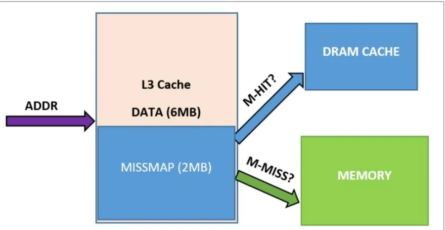
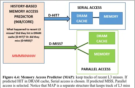
To avoid these many tag transfers during a cache miss, they also proposed a miss
predictor implemented in a data structure called Missmap. The intended purpose of Missmap
is to avoid DRAM cache access on a cache miss and therefore removing few cycles from miss
penalty. By predicting if the request will be a miss, tag access will not be a prerequisite to the
main memory request. They based the idea of missmap on the purpose of tag lookup: the first
use of tag access is to determine the existence of data in the cache. The second goal is to
identify the physical location of the data in the cache if it is a hit. They implemented the
missmap to fulfill the first purpose of data residency while tag located in DRAM fulfills the
second purpose of data location. At first, it makes missmap behave like a tag, but the big
difference is that tag bits are replaced by a single bit.
The bit is asserted when a new tag is allocated and cleared when existing tag is evicted.
Using one single bit allows for many tags to be tracked outside the DRAM cache. But because
a cache as large as 256MB can contain many millions of cache lines, this missmap can quickly
reach the order of megabytes. Their proposed improvement involves an additional large SRAM
for their experiment setup. They suggested using a portion of L3 cache for missmap space (e.g.
2MB on 8MB L3) as captured in figure 4.2. It increases overall access latency because each
request still selooks up a large L3 whether it's a miss of hit. It is important to mention that this
missmap is simply a predictor, meaning that there can be a bad prediction. Either false positive
(e.g. predict data present in DRAM cache, but it is not) or false negative (e.g. predict data is
The false positive cannot cause harm to program execution. But it can directly cause a
performance degradation due to unnecessary DRAM cache tag look-up. In contrast, the false
negative can cause damage to program execution. The off-chip data return can overwrite dirty
block without proper writeback. To remedy this issue as well as the size overhead, they
proposed a small predictor similar to a branch predictor. This predictor has a self-balancing
dispatch that can speculatively send a request to off-chip regardless of the correctness of
decisions [39]. They claimed to have observed performance improvement due to this predictor,
but we are not implementing any predictor in our methodology.
According to their simulation setup, their proposed compound-access as depicted in
figure 4.1 (a) combined with missmap as described in figure 4.2 produced a speed-up of 1.55
on average compared to baseline memory hierarchy as outlined in figure 4.1 (c). The
impractical SRAM-tag of figure 4.1(b) provided better improvement at 1.65 speedup due to
the fact that 100% DRAM space is used for data area as all the tag space in mapped in external
large SRAM. This comparison is for evaluation purpose only to show that tag-in-DRAM can
reach within 90% performance of ideal case while remaining practical and cost efficient.
One more thing to mention is that even though the missmap may speed up memory
access on a DRAM cache miss, the tag access cannot be entirely bypassed as they claimed.
Because besides the two tag lookup purposes mentioned above, evicted block need to be
determined and also if dirty, the write back is to be scheduled. Therefore, the tag access will
still occur although outside the memory access critical path. But energy consumption within
DRAM cache is not avoided because of miss predictor. It is the additional reason why we are
not implementing any predictor in our methodology as we are also focusing on the energy
![Figure 2.3. [9]. H & P Clock Frequency trend . 1986-2003 is the Golden-Age: 40%/year, 2003-present, frequency is flat: from 2005-](https://thumb-us.123doks.com/thumbv2/123dok_us/1732122.1221261/27.612.100.532.78.429/figure-clock-frequency-trend-golden-age-present-frequency.webp)
![Figure 2.4. [9]. H & P Processor-Memory Gap. CPU vs. Memory performance (Average memory requests/sec vs](https://thumb-us.123doks.com/thumbv2/123dok_us/1732122.1221261/28.612.95.537.100.412/figure-processor-memory-memory-performance-average-memory-requests.webp)
![Figure 3.1. ITRS Cross-section of wire scaling. From low metal level to global wiring, Metal 1 and intermediate wires have low-pitch and high congestion increasing capacitance and hence power consumption [5]](https://thumb-us.123doks.com/thumbv2/123dok_us/1732122.1221261/39.612.91.539.96.364/figure-section-scaling-intermediate-congestion-increasing-capacitance-consumption.webp)