WESTERN
DIGITAL
MCP-1600
MICROPROCESSOR
SYSTEM
'
MCP-1600
MICROPROCESSOR
USERS
MANUAL
WESTERN
g5
DIGITAL
C O R P O R A T I O N
© Western Digital Corporation, 1975
3128 RED HILL AVENUE P.O. BOX 2180 NEWPORT BEACH, CALI FORNIA 92663
Paragraph 1.1
1.2
1.3 1.4 2.1 2.2 2.3 2.4 2.5 2.6 3.1 3.2 3.3 3.3.1 3.3.2 3.3.3 3.3.4 3.3.5 3.3.6 3.3.7 3.3.8 3.3.9 3.3.10 4.1 4.2 4.2.1 4.2.2 4.2.3 4.2.4 4.2.5 4.2.6 4.2.7 4.3 5.1 5.2 5.3 5.3.1 5.3.2 6.1 6.2 6.3TABLE OF CONTENTS
SECTION I, GENERAL SYSTEM CONFIGURATION
General. . . . Unique Features of the MCP1600. Areas of Application
Block Diagram . . . .
SECTION II, SYSTEM COMPONENTS
General. . . . Registers
I nstruction Address Generation. Microinstruction Bus .
Data Access . . . . Microinstruction Storage
General. . . CPU Operations Control Lines. Register Load. Load Flags. . Load High Byte Load Lo Byte Modify Lo. Modify Hi .
JXX . . .
Load Literal Double/Single. Load TR
SECTION III, CPU OPERATIONS
SECTION IV, PROGRAMMABLE TRANSLATION ARRAY
General. . . PTA Components Locati on Counter Array #1
Array #2 Array #3 Array #4
Translation State Register Translation Register. . .
Programmable Translation Array Operations
I nstruction Repertoire. . Instruction Types
SECTION V, MICROINSTRUCTIONS
MCP 1600 Micro-I nstruction Set Table of Microinstructions . .
Summary of Micro-Instruction and Status Flags
SECTION VI, MICROINSTRUCTION BUS OPERATION
General. . .
Micro-I nstruction Bus Operation . . . . Micro-I nstruction Bus Element Description.
Paragraph 6.3.1 6.3.2 6.3.3 6.3.4 6.3.5 6.3.6 6.3.7 6.4 6.5 6.6 7.1 7.2 7.2.1 7.2.2 7.2.3 7.2.4 7.2.5 7.3 7.4 7.5 7.5.1 7.5.2 7.5.3 7.6 7.6.1 7.6.1.1 7.6.1.2 7.6.1.3 8.1 8.2 8.3 8.4 9.1
TABLE OF CONTENTS
(con't.)
M I BOO - M I B 10
MIB11-MIB14 MIB15
MIB16 . . . MIB17 . . . M I B 18 - M I B21 Wait Line . Data Chip . . Control Chip . Micro-I nstruction ROM
SECTION VI, (con't.)
SECTION VII, DATA ACCESS
General. . . . I nput/Output Instructions Read Instructions
Write Instructions I nput Instructions Output Instructions.
I nterrupt Acknowledge Instructions Data/Address Lines. . . . . Control Lines. . . . Interrupt, Reset, and Compute. Reset. .
Compute
Interrupts . . . . . I nput/Output Operations Standard I/O Sequence Write/Output Sequence Read/I nput Sequence . Read/ModifvlWrite Sequence
SECTION VIII, ELECTRICAL SPE:CIFICATIONS
General . . . .
CP1611 B Microprocessor Data Chip . . CP1621B Microprocessor Control Chip . CP1631B Microprocessor MICROM Chip
SECTION IX, PIN ASSIGNMENTS
Page 6-2 6-3 6-3 6-3 6·3 6-3 6-4 6-4 6-5 6-5 7-1 7-1 7-3 7-4 7-6 7-9
7 -11
7 -11
7-12 7-13 7-13 7-13 7·13 7-13 7-13 7-14 7-14 7-15 8-1 8-1 8-6 8-11
Figure No. 1-1 1-2 2-1 3-1 3-2 3-3 3-4 3-5 3·6 4-1 4-2 4-3 4-4 4-5 4-6
4-7
4-8 4-9 4-10 4-11 412 4-13 4-14 4-15 6-1 6-2 6-3 6-46-5
7-1 7-27-3
7-4
7-5 7-6 7-7 7-8 7-9 8-1 8-2 8-3 8-4 8-5 8-6 9-1 9-2 9-3Table No.
4-1 4-2 6-1
ILLUSTRATIONS
MCP1600 Microprocessor Block Diagram Simple Microprocessor System
Register Fil e _ 01 Data Paths _ 02 Data Paths _ 03 Data Paths _ 04 Data Paths.
04 Data Paths, Second Cycle_ Major Control Lines
PTA Component Interconnections . Array #1 Organization. . . Typical Gate - Array #1 . . Array #1 Data Specification. Array #2 Organization.
Array #2 Gate and I nterconnect Structure Data Specification .
Array #3 I nterrupt Organization
Array #3 Translation Register Organization. Typical Gate of Array #3.
Array #4 Organization. 01 Data Flow. 02 Data Flow _ 03 Data Flow. 04 Data Flow.
System I nterconnections, Microprocessor Set TTL Output Timing, CP1631B . . . . Microinstruction Bus Timing. .
Control Chip Microinstruction Bus Timing Microinstruction Bus Timing, CP 1631 B I/O Instruction Condition Testing Execution of Read Instruction Execution of Write Instruction . Execution of Input Instruction. Execution of Output Instruction Write/Output Sequence
Read/I nput Sequence . Read/Modify/Write Sequence Interrupt Acknowledge Sequence MCP1600 Clock Diagram _ 1611 Interface Timing . 1621 MIB Timing _ . . . 1621 Control Signals Timing 1631 MIB Timing. . . . 1631 TIL Timing. . .
CP1611B Data Chip Pin Assignments. CP1621B Control Chip Pin Assignments CP1631B Microm Chip Pin Assignments
TABLES
Translation State Code Outputs, 4 of 7 Translation State Code Outputs, 5 of 7 Microbus Timing.
Page No.
1-2 1-3 2-2 3-2 3-3
3-4
3-5 3-63-8
4-1 4-2 4-2 4-3 4-3 4-4 4-5 4-64-7
4-7
4-8 4-10 4-11 4-12 4-13 6-1 6-46-5
6-6
6-7 7-27-3
7-57-7
7-10 7-14 7-15 7-15 7-16 8-2 8-3 8-78-8
8-11 8-12 9-1 9-1 9-1Page No.
PREFACE
USING THIS MANUAL
This manual is intended to be used by those who need a detailed description of the internal operation of the MCP1600 Microprocessor Set. Users in this category are usually those who are implementing their own micro-code structures and thus require a detailed knowledge of the machine.
- Sections 2,3,4 and5 are of interest to the overall system architect
- Section 6 is of interest to the sophisticated user who will attempt to hookup to the M I B - Section 7,8, and 9 are of interest to the interface designer
If you are not sure of your need for information, the attached flowchart may be of assistance. Contact a WOC Applications Engineer Representative for any additional information.
Nu
[XII
Controller
Or Emulation
MIcro Contrall!::r
See
Users Manual
and/or See ~lcroprogramrlllng
Manual and/or
Software Reference
Manual
Ar.'
VOII E:villlldllfl\1 Yt'$ Thl'MCP1600
Nu
Art' YOII GOII1\J Tn lh!' Thl'
MCP1600
Y,'s
Art'
You Usmg Macro
Set
N"
Emulation
See Ustlrs Manual SEX-tl(m 4.0,
For PTA Programming, Microprogramming Manual and Systems
Software Refer."ce
Manual
s('!' Mep 1600
Produu
DI~sLrIPtl()n
AI!' Yrill ProyrdmnllflY
Or Iflh·rtdlll1y
Pm!jrnllllTllflq
See Macro
Programming Manual
Intl'rfaunq
5tH:' USNS Manual
Smtloll 7.0, 8.0, 9 a
This is a preliminary specification with tentative device parameters and may be subject to change after final product characterization is completed.
SECTION I
GENERAL SYSTEM CONFIGURATION
1.1 GENERAL
The Western Digital MCP1600 microprocessor is an 8-bit microprogrammable computer implemen-ted with 3 MOS/LSI chips using WDe's N-channel silicon gate process. The chip set consists of the CP1611 B Data chip, the CP1621 B Control Chip, and the CP1631 B microinstruction ROM (MICROM) chip.
These chips are interconnected by the 22 bit Microinstruction Bus (MI B) which provides bi-directional communication between the chips for addresses and instructions. A Data Access Bus provides a 16 bit port for communicating with other system components such as memory and I/O.
The I ist below describes the pertinent aspects of the set:
• 8-bit I nternal Organization
• 16-bit Data Access Port to Memory and I/O • 26 Registers
• Extensive Microinstruction Set Including Decimal Operations • Single and Double Byte Operations
• Micro and Macro Level Condition Flags • 512 Word x 22-bit Control ROM
• Control ROM Expandable to 2048 words • Micro Level Subroutine Capability
• Programmable Translation Array for Macroinstruction Interpretation • Four External I nterrupts and Three I nternal Interrupts
• External I nstruction Set
• Power Supplies +12V, +5V, and -5V
• 3.3 MHZ Four Phase Clock (Also available in 2.75 and 2.2. MHz versions) • TTL Compatible 3 State Interface
The MCP 1600 Microprocessor Set is easi Iy interfaced to a variety of appl ications through many of the standard product offerings of Western Digital and other semi-conductor companies.
1.2 UNIQUE FEATURES OF THE MCP1600
The MCP 1600 has two uncommon and usable features that set it apart from the standard run of MOS microprocessors.
The MCP1600 is 'a vertically microprogrammable processor.
The MCP1600 has a programmable translation array which quickly and auto-matically generates the jump vectors required for emulation and macroinstruction applications.
The unusual feature of being able to decode macroinstruction quickly and automatically sets the MCP1600 apart from other devices in the microprocessor market.
Unlike other offerings in the MOS microprocessor marketplace, the MCP1600 can be applied to problems that demand speed for their solution. The combination of speed (maximum 3.3 MHz instruction rate) and high density (thus great processing power) brings the economic advantages of MOS to bear upon problems which previously could only be attached by bipolar microprocessors or special logic designs.
Careful review of the contents of this manual will stimulate the imaginative user to think of many applications to which these unique features can apply significant advantage.
1.3 AREAS OF APPLICATION
to be determined by data, if desired. This makes the MCP1600 highly suitable to areas of appli-cation that require a substantial amount of data decoding. Such appliappli-cation might be:
The emulation of an existing computer's instruction set. The invention of a new, application oriented instruction set. The construction of a macro-instruction processor
The construction of a data driven processor
Another of the attributes of the MCP1600 is its ability to quickly process data in a sophisticated manner. The availability of a rich instruction set coupled with speed and a variety of registers make the MCP1600 especially applicable to problems that require great quickness. Applications such as:
Communications Multiplexing Host computer front ends
Medium Speed Peripheral Device Control
can readily be attacked by the MCP 1600.
The MCP1600 provides still another advantage to the system designer. It is truly easy to interface. Including the processor set and all other logic a microcontroller can be implemented with as few as 15 parts. Figure 1-2 shows such a system.
Specific application notes detailing ideas relevant the application of the MCP1600 to the above men-tioned areas are available from your Western Digital sales representative.
1.4 BLOCK DIAGRAM
Figure 1-1 describes the interconnection of the required components of the MCP1600 micro-processor set. The DATA CH I P, (CP 1611 B) contains the arithmetic logic unit, the micro-instructions decode and the register file. Ad-ditionally, it contains paths to control the operation of the processor.
The CONTROL CHIP (CP1621B) contains the program translation array, portions of the control circuitry to control operation of the processor set, the microinstruction counter and the I/O control system.
The MICROM CHIP (CP1631B) contains the microinstruction ROM. The MP1600 micro-processor set may be expanded up to four MICROMs giving the user a total of 2,048 22 bit microinstructions. The simple system illustrated in Figure 1-2 shows all of the functional components needed to make a work-ing microprocessor. Note that, in addition to the three parts comprising the Micropro-cessor Set, twelve other available standard TTL parts are required. These parts serve to:
Generate the clocks
Latch and gate input signals Latch and gate output signals
This is to be contrasted with some other com-mercially available microprocessors which may require as many as 50 other parts to imple-ment a system of equivalent capability.
1-2
COMPU RESET
CS
TE (TTL) (TTL
10 (TTL)
IL~
12 (TTL) 13 (TTL)
01 0203 O4 ~
II I I
ss
00
512 X 22 ~ ROM CHIP CP1631B
-
---°,°
1
°1
3°1
4CONTROL CHIP
f--CP1621B
II
i •
•
•
•
I~ I~
....
...
N
' : i
co l-~
I-00_
~
°1°1
2°1
3j4
DATA CHIP CP1611B
WAIT
RPLY (TTL) BUSY (TTL) SYNC (TTL) DIN (TTL) DOUT (TTL) WB (TTL) lACK (TTL)
FIGURE 1-1 MCP1600 MICROPROCESSOR BLOCK
DIAGRAM
I~'S COUNT
1 74S74
1 7474
1 74174
1 7427
1 74S05
1 74S139
4 SN75361 AP
1 745124
4 8126 TOTAL 15 Ie'S
SN75361AP
'i
b
-5V +12V -5V +12V
G7D I +jV I
G'I0
I +~V IMICROM CONTROL CHIP
CP163l
I
CP1621
04 03 02 01 WAIT 04 03 02 01
G ~
!
~
-
-
~~ ~ ~ ~ ~
~~
" "
"
~ ~~~ ~-~ ~r - -
i ;-:
n
~[: :~~l'-"-'-:~.::::-~--t::+-~~~+J=HJ:t+Jj++tJ4r~Jj+-Jj-_-_-+--l---+-JT
p-~I-_q--~~-~-~'--~~~YW~--~4-4-+---~++4-~+4~~~~++4-~+4---~~
2 0 Q 12 0 Q 9 6 ~ I
574 574 74S13~2hoJ-- - " 021
11 8 13 7427
CK a CK Q 11
L ______ -I _____ 1~~ 1 - -14 04 03 02 01 WAIT 04 03 02 01
lon
!NT CLK ENABLE
~
~hr
15,:~
;; tiJ
L-22K
MICROM DATA CHIP
512x22
CP1611
2~ 3 '0
5 Q2 02 4 11
7 Q3 03 , 12
10 04 0411 13
~
'5V 12 05 0513 COMPUTE
~l
REPLY
I ~ ~p--+ ______ '~500 D6'~1~4 ________ ~~~ __ -C==~
~ '----+,- RESET
lACK
}
~ ________ 4-____ -I~ ___ ~;X74~50_5 ________ ~~ ____ ~==: ~ ____ ~ ____ ~~.v
I
DALe0 DALel DAL02 DAl03 OAL"" DAL~5 DAl6t6n" "7
DALes DAL6t9 OALl DALll OAL12 DALl3 DA 14 DALl5
V · "
v
~~
7~~ V7~:~
7427
K a K a
R R
~ 6".,
L,.JL
~
10!-i 13
8T26 - !1 -8T26 ! - !! -8T26
:1-' - - SIG. 8126 w. DIN oaUT SYNC BUSGRNT BURSQ XDIN BUSH Busel BUS02 Buse3 .U~ aosas BUSi6 BUS07 BUS08 ~ BUS10 BUSll BUS12 BUS13 BUS14 BUS15 MIB19 MfB2B MlR21
}
' -INTERRUPT LINES SYSTEM CONTROL LINES DMA CONTROLS MACRO BU5 :2:w
I-en >-enec
0 en~ en
w
...
Uw
0ecec
C?
::>0..
0 0
SECTION II
SYSTEM COMPONENTS
2.1 GENERAL
This section describes the main functional components of the MCP1600 system. The reader should be aware that the system is physically partitioned into three kinds of devices. He should be more interested and aware of the logical partitioning of the system, which encompasses five areas:
Processing and data handling. This is generally handled on the CP1611 B Data Chip. Next I nstruction Address Generation. This is generally handled on the CP 1621 B Control Chip.
Microinstruction Storage. These are contained on one or more CP1631 B Microin-struction ROMs.
Microinstruction Bus. This bus connects the three types of devices together and pro-vides a path for the microinstructions to flow from the microinstruction ROM to both the Control and the Data Chip.
Data Access Bus. Th is bus provides access from the MCP 1600 microprocessor set to the outside world. Lines comprising this data access bus come from all three of the chip types. Lines containing the address and data come from the Data Chip, control lines defining the state of the data access come from the Control Chip and user programmable control lines come from the Microinstruction ROM.
While not strictly a logic component, the clocking scheme should be noted here.
The MCP1600 operates on a four phase clock system. While there are some variations, the general use of each phase period is:
01 I nstruction Access 02 Data Access 03 Execution 04 Data Update
The clocking scheme can be more easi Iy understood by reference to secti on
III
and sectionVIII.
This section will describe the functional components that make up these partition areas.
2.2 REGISTERS
This section will describe data handling registers in the MCP1600 set of interest to the system designer.
Register File. The Register File consists of 26, 8 bit registers which provide RAM data stor-age for the MCP1600 processor set. The register file has 2 output ports and 1 input port. Fourteen of the registers of the file can be directly addressed by the A and/or B register de-signators of a microinstruction. Additionally, the 16 top-most registers of the register file may be considered as register pairs and can be addressed by, the G register (see below) to permit operation on full words of data. The Register File is on the Data Chip.
The A and the B output ports of the register file feed into the ALU.
G register. The G register is a pointer register on the Data Chip that describes the currently accessed linked consecutive pair of registers in the register file. Figure 2-1 describes the inter-action between the G register and the register file. Note that, when the G register is being used, access to the register file is from the top down. Thjs is opposed to the access to the re-gister file when only the A and B fields are being used as designators, in which case it is from the bottom up. This register is loaded by IW and LGL instructions. "Input Word" instruc-tion loads the G Register from the DAL bus as specified by the "b"field of the instrucinstruc-tion. "Load G Low" instruction loads the G Register Ra.
are addressable from either the G or the M I R registers. Figure 2.1 describes the addressing conventions of this file. It is helpful to note that if the a or b fields of the MI Rare 1 or 0, then this enables G-Register addressing.
Some Examples
Assume G
=
4, a=
0, b=
BThen one operand (A Port) will be from G'8' The other operand (B Port) will be from R'8'
Assume G
=
0, a=
7, b=
1Then one operand (A Port) will be from R'7' The other operand (8 Port) will be from G'1'
Assume G
=
6, a=
1, b = 0Then one operand (A Port) will be from G'D'
The other operand (B Port) will be from G'C
Assume G
=
3, a=
6, b=
AThen one operand (A Port) will be from R'6' The other operand (B Port) will be from R'A'
- Assume G = 5, a = 0, b = 1
Then one operand (A Port) will be from G'M The other operand (B Port) will be from G' B'
REGISTER FILE ADDRESSING MODES
Bottom
R2 R3
R4
R5 R6 R7
R8
R9 RA
RS R~/(;~ RD/GD
RE/GE
RF/GF
GB GA
G9
G8
(;7 G6 G5
G4
G3
G2
Gl
Top (;01
,1"
FB Port~
{
0 0 a~lorb~l
and
G ~
a -
5ALU Status Bits. The ALU provides 4 status bit outputs which reflect the result of each 8 bit operation. The ZB and NB bits are updated after every ALU operation. C4 and C8 are updated for Arithmetic or Shift operations. These bits may be tested by Jump but their primary function is to pass result data from the first cycle of a word instruction to the second cycle.
The available status bits are:
ZB: Set if the result of a Byte or Word operation is zero; cleared otherwise.
NB: Set if the high-order bit of a Byte or Word operation is a one; cleared otherwise (except for SRW and SRWC).
C4: Set if Carry Out of Position 3 is a one; cleared otherwise. Updated only on Arithmetic operations. This status bit is used mainly for decimal arithmetic corrections.
C8: Set if Carry Out of Position 7 is a one; cleared otherwise. (Note that this status bit is not set to borrow for subtract as is the case with the C Flag.) Also set if the shifted off bit of a Shift operation is a one; cleared otherwise.
Condition Flags. The Condition Flags consists of 4 latches which can reflect the status of the previous ALU results. The updating of these flags can be selectively enabled or disabled at the discretion of the mi-croprogrammer. The condition flags are updated with odd-numbered instruction opcodes in the range of 80 -EF.
Z Flag: Set if the result of a Byte or Word operation is zero, cleared otherwise.
N Flag: Set if the high-order bit of the result of Byte or Word operation is (except for SRW and SRWC) is a one; cleared othewise. (Note that this is the complement of the sign of the result if over-flow occurs.)
C Flag: Monitors the carry, borrow and shifted off bits as follows:
Add and Increment:
Subtract and Decrement:
Shift:
Set if there is a carry from the most significant bit of the Byte or Word result; cleared otherwise.
Set if there is a borrow (complement of carry) from the most significant bit of the Byte or Word result; cleared otherwise.
Set if the bit shifted off in a left or right shift is a one; cleared otherwise.
The C Flag is not affected for operations (other than those listed above) even if the other flags are updated.
V Flag: Set if there is an arithmetic overflow on Arithmetic operations. Cleared if there is no overflow and on Non-arithmetic operations. On Add operations overflow occurs when the sign of the two oper-ands are the same and the sign of the result is different. On Subtract operations overflow occurs when the signs of the two operands are different and the sign of the result is different from the operand in Ra (V=C7
a3
C8).The format of the ALU status and flag register word is shown below:
NB
ZB C4 C8 NZ
v
C7 6 5 4 3 2
o
MI R Register. The 16 bit MI R register holds the least significant 16 bits of the 22 bit microinstruction currently being executed. The MI R register is loaded every 01 unless the currently executing microin-struction is of the 2 cycle variety. In th is case the register is not clocked on the second occurrence of 01.
2.3 INSTRUCTION ADDRESS GENERATION
This section describes the register and arrays used in generating the next microinstruction address.
Location Counter Register. The Location Counter (LC) is an 11 bit register which holds the address of the next microinstruction to be accessed. Under normal conditions, the LC is incremented by one after each access of a microinstruction. The LC can be altered by other than one by execution of a Jump instruction or a Return from Sub-routine (RFS) instruction or by invoking a PTA translation.
Return Register. The Return Register (RR) holds an 11 bit address and permits a subroutine depth of one in the microprowam. When a subroutine jump is indicated (MI B 16 = 1) the return register stores the incremented contents of the LC. Contents of the Return Register can be transferred to the LC under the control of a RFS - (Return From Subroutine).
Translation The Translation Register (TR) is a 16 bit register which holds the data presently being input to the PTA. Data on the Microinstruction Bus (MIB) is used to load the Trans-lation Register. Note that only the upper or lower half of the TransTrans-lation Register can be fed into Array 3 at one time.
Translation Arrays. There are four arrays on the control chip that control the generation of the next microinstruction address. They generate new inputs into the LC register, as a function of the LC register contents, the contents of the translation register, interrupts, and other miscellaneous
inputs. The detailed operation of these arrays is.discussed in Section 4, PROGRAMMED TRANSLATION ARRAY OPERATIONS.
2.4 MICROINSTRUCTION BUS
The Microinstruction Bus serves to interconnect the three required parts of the MCP1600 Microprocessor set. The bus is organized into 4 distinct sections:
MIBOO - MIB15 carry proper microinstruction data from the microinstruction ROM chip to both the control chip and the data chip. These lines may also carry data between the data chip and the con-trol chip under certain conditons.
M I B 16 controls the subroutine jump operation. When M I B 16 is set on a jump instruction, it causes the incremented contents of the LC register to be placed into the Return Register.
M I B 17, if set, causes the PTA on the Control Ch ip to perform a Read Next I nstruction translation.
MIB18 - MIB21 are TTL level outputs that can be programmed by the user as his needs dictate. They are not used by the MCP 1600 Microprocessor set to control its operations. They are provided for the conven ience of the user in order that he may interface to the M I B bus or control devices directly from the microprogram level.
2.5 DATA ACCESS BUS
The Data Access consists of three sections:
DALOO· DAL 15 carry address and data between the data chip and the outside world.
Outside Control Lines. There are five TTL level Outgoing Control Lines that inform the outside world of the present state of the MCP1600 set. These signals inciudeSync, Input Instruction, Output Instruction, Interrupt Acknowledge, and Write-Byte.
I ncom ing Control Lines. There are 8 TTL level I ncoming Control Lines. These incoming control lines inform the MCP1600 Microprocessor set of the state of affairs in the outside world. There are four interrupt lines, a Compute line, a Reset line, a Reply line and a Busy line.
2.6 MICROINSTRUCTION STORAGE
MICROM
SECTION III
CPU OPERATIONS 3.1 GENERAL
This section describes the internal workings of the Data Chip, the CPU of the MCP1600 system. Its purpose is to provide the designer with a background understanding to enable him to more effectively interface with the Micro I nstruction Bus and the Data Access.
The description of the MCP1600 Processor must proceed from the knowledge that there are two important and distinct partitions to the processor. The first partition, called the Data Chip, pro-vides classical stored program processing. The Data Chip consists of:
A register file
An arithmetic logic unit A M icroi nstruction register A register file address decoder A control signal generation function Condition flags
Jump decoding I nput/Output gating
The data chip is responsible for data manipulation as a result of instruction execution.
The second partition, the Control Chip, generates address data that directs the accessing of the next microinstruction to be executed. This address generation mechanism provides the MCP1600 with its unique emulation capabilities. While the Data Chip is executing the presently fetched microinstruc-tion, the Control Chip is performing a transformation upon the presently executing macroinstruc-tion to determine the address from which to fetch the next microinstrucmacroinstruc-tion to be executed.
3.2 CPU OPERATIONS
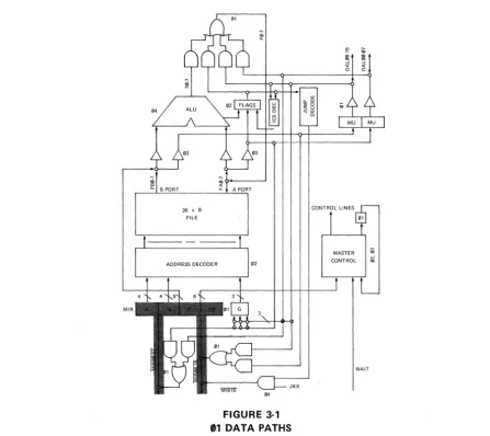
We start the CPU operation description by first assuming that the machine has been properly reset and has just entered the compute mode. The Control Chip will cause microinstruction to be fetch-ed from the MICROM to be placfetch-ed on the MIB bus. (See Figure 3-1) Assuming that the clock is now on the lead ing edge of
0
1, the contents of the M I B bus are gated into the M I R register on the Data Chip and the MI register on the. Control Chip.MIR
FIGURE 3-1 01 DATA PATHS
W 0..0
::;0
"U
~~
WAIT
At the end of 0 1 (trail ing edge of the clock), the contents of the M I R register have settled. The
contents on the M I R register are held fixed until the next occurance of
0
1 (four phase times).At the beginning of 02, the contents of the M I R register are presented to the various different functions of the CPU. The A and B fields are presented to the address decoder, as is the G re-gister. The contents of the M I R register's C field and OP field are presented to the master control function of the Data Chip. During 02 and 03 the master control function decodes the C field and generates signals which control' the gating of data to the various functions of the Data Chip. Also during 02 the address decoder is interpreting the contents of the A field and the B field and accessing the appropriate register in the register file. Also during 02 the condition codes reflecting the result of the last ALU operation become valid. They are presented to the FLAGS register which retains them for examination on the next occurance of 04. Figure 3-2 illustrates
...
s
'"
L1- B PORT
26 x 8 FILE
...
~a.---'
L1- A PORT
04
FIGURE 3-2
o
2 Data PathsW 0.. 0
~o =>u
..., w
o
It)
~
..J
<t
o
CONTROL LINES
Phase 3 is the register access phase. Dunng 03 data is presented to the ALU by the A and the B output ports of the register file. Data may also be presented to the ALU B port by means of the literal path from the MIR register. Note the literal path (whose contents are the C and B field of
the MI R) bypasses the address decoding logic and the register file. Also during 03 the contents of the A and B register file output ports may be presented to the Data Access on line DALOO --DAL 15. Also during this phase time the contents of the register file A port may be presented to the flag register. Finally, during this phase time, the contents of the register files A and B ports may be presented to the gating which controls access to the M I B bus. Figure 3-3 illustrates
01
...
6. LL
'---',~-- JXX
FIGURE 3-3
o
3 Data Paths04
LJ.J
Cl. 0
:;;:0 ~U
--, LJ.J
o
LO
cO e
...J
«
o
MASTER CONTROL
...
e 6. e
...J
«
o
WAIT
MIR
""
&. en
u.. B PORT
26 x 8
FILE
ADDRESS DECODER
01
""
~ 0<01---'
u.. A PORT
02
'---'r--- J xx 04
FIGURE 3-4
o
4 Data PathsUJ
,,-0
::;;0 ::J U
-, UJ o
CONTROL LINES
MASTER CONTROL
WAIT
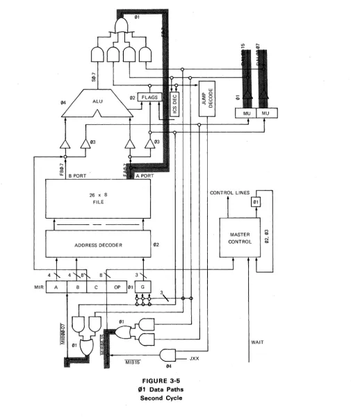
If however, the instruction requires two cycles for execution, things proceed differently. At the begi nning of 0 1 of the second cycle, the contents of the M I R are preserved, no new data is gateo in. The low order bits of both the 'A' and 'B' fields are complemented to access adjacent slots in the register file to those previously addressed in the first cycle. Also during this phase, the CPU may output data to the MIB bus. Figure 3-5 illustrates this path.
Other than these exceptions, two cycle instructions proceed as do one cycle instructions.
MIR
26 x 8 FILE
ADDRESS DECODER 02
04
FIGURE 3-5
~1 Data Paths
Second Cycle
JXX w
a. Cl
~o
::l U
....,w
Cl
CONTROL LINES
M
MASTER S CONTROL
3.3 CONTROL LINES
During
02
and03
the Master Control function is decoding the new contents of the MI R register in order to generate signals to control the data transfers described above. These control signals are generated on the basis of the contents of the C and OP fields of the M I R register. All of the control lines generated by the Master Control function are not described here because some of them serve timing and sequencing functions that are not necessary to the understanding of the CPU operation and how it affects the Data Access and Microinstruction Bus. However, there are several control lines which the designer may find helpful to understand. They are shown in the attached diagram, Figure 3·6, and, in order, they are:3.3.1 REGISTER LOAD
This control line determines whether or not the output of the ALU will be gated back into the register file input port. It is invoked by register to register format instructions.
3.3.2 LOAD FLAGS
This line controls whether or not the output of the FLAGS register will be gated into the register file input port. It is generated by the Load Flags and Copy Flags instruction.
3.3.3 LOAD H I BYTE
This control line determines whether or not the contents of the DAL08-15 will be gated into the register file input port. This line is controlled primarily by the Input class of instructions.
3.3.4 LOAD LO BYTE
This control line determines whether the contents of DAL-07 will be gated into the register file input port. It is generated by input class instructions. Note that this signal and preceeding signal are generated by the specification in the B field of the appropriate input instruction. Note also that one can input the low order byte, the hi order byte, or both bytes. This latter case is an Input Word Instruction.
3.3.5 MODI FY LO
This control line is invoked by the Modify instruction and causes the output of the A register file port to be gated on to the low order 7 bits of the microinstruction bus. This control line is also invoked by the Load Translation Register instruction.
3.3.6 MODIFY HI
This control line is the high order analog of the previously described control line.
3.3.7 JXX
This control line is invoked by the jump instruction. It is made hi during the first phase four of the jump ,instruction, if the jump instructions have been met. It causes the contents of the MI register on the control chip to be placed into the LC register.
3.3.8 LOAD LIT
....
s
x
x
...,
3.3.9 DOUBLE/SINGLE
This control line is generated by the Master Control for use by itself. It is invoked by instructions that require two cycles for execution. In the main, it controls whether or not a new instruction is gated into the MI R register at the next occurance of (/) 1.
3.3.10 LOAD TR
This control line is invoked by the I nput Word instruction if either bits 4 or 50f the B field are set. These bits being set will cause the data on the Data Access to be placed into the translation register on the Control Chip. It is in this fashion that new macroinstructions are fetched from the user memory for decoding.
LITERAL DATA
----r-...,
LOAD LIT
B PORT OUTPUT ALU OUTPUT
MIB00-07
r - l - - - -
MODIFY LO A PORT OUTPUTr - l - - + - - - L O A D T R LOAD LIT
REGISTER LOAD ~AlL~U.sO~U!.:!T!P~UIT~==::L_~
L-_ _ _ _ _ LOAD TR DAL08-15
L...---MODIFY HI
B PORT OUTPUT
WAIT
MASTER CONTROL
CONTROL LINES
LOAD FLAGS FLAGS OUTPUT
LOAD HIBYTE _::::DA=L0::::8~-1:.::5:-_'::;"'-1_~ LOAD LOBYTE _.::.D;..:A.::.L0:;,;0:...-0:..;7 _ _ '-;-I_J
A PORT INPUT
01
DAL0B·15 DOUBLE/SINGLE
FIGURE 3-6 MAJOR CONTROL LINES
3-8
4.1 GENERAL
SECTION IV
PROGRAMMABLE TRANSLATION ARRAY (PTA)
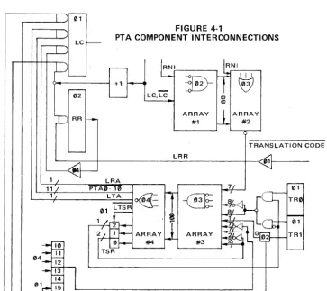
This section describes the operation of the MCP1600 Microprocessor set's most unique feature, the Programmable Translation Array. The Programmable Translation array serves to generate new micro· instruction fetch addresses as a function of several parameters. These parameters are those which are normally considered during the decode of a macroinstruction. While the Programmable Translation Array was designed specifically to eliminate most of the over head of macroinstruction translation, it is useful for other purposes. One could, for instance, conceive of a data driven processor that would determine the next operation to be performed on a data structure as a function of the present data and the present operation. The uses of the Programmable Translation Array are limited only by the system designer's imagination.
Briefly, the Programmable Translation Array consists of eight elements. They are:
Location Counter. Array 1
Array 2 Array 3
Translation Register Array 4
Translation State Register Return Register
These elements give the capability of calculating microinstruction addresses other than sequentially, or as specified by a jump instruction. Figure 4-1 depicts their interconnection. The mapping (or new Location Counter value) that the PTA generates, when invoked, is a function of the value of the Location Counter, the contents of the Translation Register, the interrupts, and the state of the R N I line.
11
01
LC
02 RR
FIGURE 4-'
PTA COMPONENT INTERCONNECTIONS
+1
LC,LC
ARRAY #1
LRR
ARRAY #2
TRANSLATION CODE
~--__
--~---~--<01~---LRA PTA0· 10
L~o<g=
01 LTSR
-01
TR1
4.2 PTA COMPONENTS
This section will describe the components of the Programmable Translation Array and their functions.
4.2.1 LOCATION COUNTE R
4.2.2
It is the function of the Location Counter to hold the address of the next microinstruction. The Lo-cation Counter is 11 bits wide and has outputs to M I BOO-M I B 1 0 and to Array # 1. I t has inputs from the Master Control function, Array #4 and the Return Register. There is also an' input to the Location Counter from an incrementer.
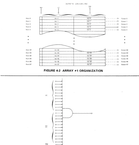
ARRAY #1
Array #1 is an 88 element array of active low input AND gates with 23 inputs There are 11 true inputs and 11 complemented inputs from the Location Counter and the RNI bit (MIB17). Figure 4-2 illustrates the organization of Array #1. Figure 4-3 illustrates the concept, as opposed to implementation of a typical gate, one of 88, that make up Array #1. The outputs of these gates make up the bulk of the inputs of Array #2.
Word 0
Word 1
Word 2
Word 3
Word 4
Word 82
Word 83
Word 84
Word 85
Word 86
Word 87
OUTPUT N LeN· LeN. RNI
I-+ _ _ _ _ A.._d __ ' o'--_ _ _ _
+--___
---'Ad'-' 0"--_ _ _ --..1 - - - C> Output 0 H _ _ _ _ "'Ad'-':...' _ _ _ _ -+ _ _ _ _ :..:.Ad::.'.:..' _ _ _ _ --j - - - C> Output 1 H _ _ _ ---'A.=dc.:' ' ' - -_ _ _ _ t---_ _ _ ~Ad'=' :::-' _ _ _ _ -1 - - - -C> Output 2Adr 3 Adr 3 Output 3
H _ - - - = = _ A - d - ' 4 _ _ --=:::-_t---_ _ _ _ Ad_, 4 _ _ _ _ ---11 - - - -C> Output 4
-~
~~---~
--... ...
---~
---Adr 82---~ - - - [> Output 82
Adr 83 Adr 83 - - - C> Output 83
Adr 84 Adr 84 - - - C> Output 84
Adr 85 Adr 85 ______ c> Output 85
Adr 86 Adr 86 - - - C> Output 86
Adr 87 Adr 87 - - - C> Output 87
FIGURE 4-2 ARRAY #1 ORGANIZATION
LC
LC
RNI
FIGURE 4·3 TYPICAL GATE· ARRAY #1
The purpose of Array #1 is to perform a selection function. When the inputs to Array #1 match one (or more) of the word values (addresses) the output associated with that word is asserted. This array is programmed with 6 hexidecimal digits as shown in Figure 4-4. Transistors are placed in the array for 1 bits in the data specification. To program a group of addresses the bits of the address to be left out are specified as (/) bits for the true and complement address inputs. This produces a 'DON'T CARE' effect for those bits and the result will always be a match. This lets the user match on mo-dulo address.
The R N I I ine serves to inhibit the output of array # 1. The reason tor this is described later.
o
LC
ADDRESS1 01
LC
ADDRESS23 22 1 2 11 10 0
Example:
Address
=
X' 5F8'Array #1 Data Word
=
X' 5F820TFIGURE 4·4 ARRAY #1 DATA SPECIFICATION
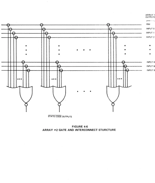
4.2.3 AR RAY #2
Array #2 is an ORed array whose outputs are negated. The array has 89 inputs, 88 from Array #1 and one from MIB17, the RNI line. The seven outputs from Array #2 represent a translation state code and be-come inputs into array #3.
Figure 4-5 illustrates the orgainzation of Array #2. Figure 4-6 illustrates in some detail, the concep-tual structure of the gate and interconnect structure of Array #2. The small circles present where the lines would normally cross represent connections that can or cannot be made. It is via the making or not making of the connections with transistors that this array is programmed.
Alr,l, #1 Out!JL:t~
RNI 111Pl,t
C>-l>
--C> -
C> -C> --
C>--RN I Sldte Codt'
Slale Cod .. 0 Slate Cutie 1
Slate Co(le 2
SIdle Code 3
S1dle Coch" 8l State Code 82 Stilte Code 83 C> - - - --f-_---'S"'''''-W .::.:;C'""d,-=-84--1
C> - - - State Coele 85 ;> - - - - SU"-t' Cod!' 86 f - - - l
C> - - SIdle Code 87
Slate Code OutPlll
1""t. r .
,..
--
I - I "r .
-
-,..
-
,..
•
•
•
•
•
•
•
•
•
•
•
•
r.
,.
-r .
-
...
,.
Ir..-
Ir.•••
•
••
•••
...
_ _ ...-1.
--
-'" ' - L..- ... --'"•
•
•
STATE CODE OUTPUTS
FIGURE 4-6
ARRAY #2 GATE AND INTERCONNECT STURCTURE
Array #2 is driven by the inputs from Array # 1. When one or more outputs of Array # 1 are asserted, Array #2 will make the corresponding word available as its outputs.
The purpose of Arrays #1 and #2 is to provide a mapping between the present value of the Location Counter and a preselected set of translation state codes.
ARRAY 1 OUTPUTS
RNI
INPUT 0
INPUT 1
INPUT 2
•
•
•
INPUT 85
INPUT 86
Due to electrical considerations, there are restrictions placed on the configuration of Array #2. Nor-mally this array is programmed in a 4 of 7 code (4 of 7 outputs may be selected to be high, the other 3 must be low), or more ideally, to reduce capacitive loading, a 5 of 7 code. The tables below describe the various state code outputs available in both the 4 of 7 and the 5 of 7 schemes.
0F 20 3C 56 69
1F 30 58 68 75
17 2E 47 59 6A
2F 3E 50 60 76
18 33 48 5A 6C
37 4F 5E 6E 79
10 35 40 5C 71
38 57 67 73 7A
1E 36 4E 63 72
7C
27 39 53 65 74
28 3A 55 66 78
Table 4-1 Translation State Code Outputs -- 4 of 7 Table 4-2 Translation State Code Outputs -- 5 of 7
The outputs of Array #2 represent some of the inputs to Array #3.
The RN I line (M I B 17) deserves mention at th is point. I t is the purpose of the RN I Ii ne to force a particular user defined state code from the mapping represented by Arrays #1 and #2. This state code will be independent of the contents of the Location Counter.
Accordingly, RNI inhibits the outputs of Array #1 and invokes that state code selected by the user in Array #2 and makes it present at the output of Array #2.
The programming of Array #2 is illustrated in Figure 4-7 below. Transistors are put in the arrays for zero bits as per the data specifications.
o
7
6
Translation Code
Example:
o
x'
56'4.2.4 AR RAY #3
Word
a
Word 1Word 2
Word 3
•
•
•
Word 14 Word 15
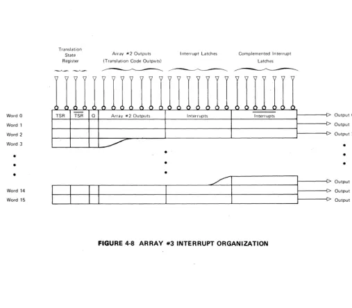
Array #3 consists of 100
active
low input AND gates, and has 42 inputs. In contrast to Arrays #1 and #2, the inputs come from a variety of sources. The inputs to this array constitute a direct interface to the real world at the macromachine level, as one of the inputs is the translation register. The inputs to Array #3 are:Seven
from Array #2. {Translation Code}Sixteen from the Translation register. Eight are true data and eight are complemented data. Fourteen inputs from the interrupt latches. Again, both true and complemented data are pre-sent.
Two from the translation state register. Again, both true and complemented data are used. One input, called the Q signal, not generally usable.
It is worth noting, that, while there are 42 inputs in Array #3, they are not all present at the same time. The array is broken into two partitions. The first partition consists of words 0 through 15, and has as its inputs, the 14 bits from the interrupt latches. The second partition of the array, words 16 through
99 have,
in these same slots, the 16 bits of inputs from the Translation Register.The Figure 4-8 illustrates the structure of the first partition of the array. Figure4-9 illustrates the se-cond partition of the array. Figure 4-10 shows a conceptual picture of a typical gate in the array.
Translation State Register
TSR TSR
I
I
(
Q
I I
Array #2 Outputs (Translation Code Outputs)
( (
'>
Array #2 Outputs
~
•
•
•
Interrupt Latches
( '> '> ( (
Interrupts
./1
Complemented Interrupt Latches
( ( ( '> C
Interrupts
FIGURE 4-8 ARRAY #3 INTERRUPT ORGANIZATION
:
Output
a
Output 1 Output 2•
•
•
\Ah," 16
Word 17
Word 18
\Nord 19
•
•
•
Word 98
Word 99
T rallsl at iOIl
Stdte Register
---.~
7 - 7
( ) ( :>
TSR TSR Q
\
( (
Array #2
Outputs
(
Arrav # 2 Outouts
\
(
\
) (
T ranslat Ion Reqi ster
•
•
•
Translation
Register
7 \
I
(
\l \l 7
:, <:
Translation Reqister
FIGURE 4-9 ARRAY #3 TRANSLATION REGISTER ORGANIZATION
TSR TSR
Q
Translation
Code Outpu1S
Interrupt
Latches
Translation Register
Interrupt
Latches
or
Translation Register
Output to Array 4
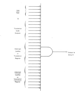
FIGURE 4-10 TYPICAL GATE OF ARRAY #3
7
Output 16
"t> Output 17
v Output 18
Array *;3, being an ANDed array, will try to match the configuration of its inputs against one of the words that make up the array. If it finds a match, the output associated with that word will be asserted.
Array #3 is programmed with true data as eight hexadecimal digits. DON'T CAREs, which always result in matches, are created by placing both true and complemented bits to zero. Below is a data specification for the programm ing of Array #3.
AND Gates
0-
15: INTERRUPTS~I N~T~E::-:R::-:R::-:U~P~T~S~J
14 8 6 0
AND Gates
16-99: TSR TSR
0 0 0
Q0
TRANSLATION
4.2.5
31 3029 2827 24 23 22 16 15 8 7
NOTE: Q= ((TR14 ·TR13· TR12)
+
(TR14- TR13 'TR12))ARRAY #4
Array #4 is a NORed array with 100 inputs which come from Array #3. The outputs generated by Array #4 include address data to be fed into the L.ocation Counter, data to be fed into the Trans-lation State Register, and three control lines. Two control lines determine whether the L.ocation Counter will be loaded from the Return Register or the output of the translation array. The third control line determines whether or not the value presented to the Translation State Register will in fact be loaded into the Translation State Register. Figure 4-11 illustrates the orgainzation of this ar-ray. Note that not all the outputs are complemented. The two control signals L. RA and L. T A are true data.
Input 0
Input 1
Input 2
Input 3
Input 4
Input 5
Input 95
Input 96
Input 97
Input 98
Input 99 Array #3
Outputs FIGURE 4-11 ARRAY #4 ORGANIZATION
Translated Address 0
•
•
•
Trans
latian Translated Address:
State
Req. Inputs to Location Counter
4~
Word 0
Word 1
Word 2
Word 3
Word 4
Word 94 Word 95 Word 96
Word 97
Word 98 Word 99
Array #4 will determine if any of its inputs are active. If they are, the word associated with the ac-tive input is placed on the output lines.
The array is programmed into terms of true data. Five hexadecimal digits are used to program each word.Transistors are placed in the array for 1 bits in the data specification. More than one active AND gate in Array 3 causes the outputs to OR.
L
L L T
0
R T S0
TRANSLATION ADDRESSA A R
19 18 17 16 15141211
o
4.2.6 TRANSLATION STATE REGISTER
The Translation State Register serves two functions. One is to determine whether the Hi or the Lo order byte of the Translation Register is to be selected for input to Array #3; The other is to provide a four state feedback as an input of Array #3. The loading of the Translation State Register is control-led by an output (L TSR) of Array #4.
4.2.7 TRANSLATION REGISTER
The Translation Registerholds the data presently serving as input to the Programmable Translation Array. It receives its inputs from the Micro I nstruction Bus (M I BOO - M I B 15) as a result of an L TR or IW instruction. Because of the fact that its output destination is 8 bits wide, only half of the Trans-lation Register can be examined at anyone time. The TransTrans-lation State Register controls which half of the Translation Register is gated into the input of Array #3, its destination. It serves as a feedback term of information to the second half of the word.
Bit 2 of the TSR controls the selection of translation input from the TR. When this bit is a zero the upper byte of the TR is selected; when it is a one the lower byte is selected. TSR2 does not serve as an input to Array #3.
4.3 PROGRAMMABLE TRANSLATION ARRAY OPERATIONS
This section describes the operation of the Programmable Translation Array. The operation is based on the description of the components in the preceeding section that make up the Programmable Translation Array. The Programmable Translation Array operates as a loop. The beginning and end points of the loop can be considered as the Location Counter.
This loop is completed within one machine cycle. It is helpful to remember that the main compo-nents of the loop are
The Location Counter
Arrays #1 and #2, which taken together perform a mapping of the Location Counter to a translation code.
The translation register, which holds the macroinstruction undergoing the translation process. Arrays #3 and #4, which take the translation code and the macroinstruction presently under-going translation and map them into an address.
This newly generated address can then point to the beginning of a macroroutine to interpret the macro-instruction presently accessed.
The following description can be best followed by reference to the attached diagrams which depict the flow of data in the Programmable Translation Array as a function of phase time clocks.
The operation of the Programmable Translation Array begins at 0 1. During 01 the location counter is loaded with its new value. The new value can come from anyone of four sources. They are:
From Array #4 of the Programmable Translation Array From the M I register
From the incrementer From the Return Register
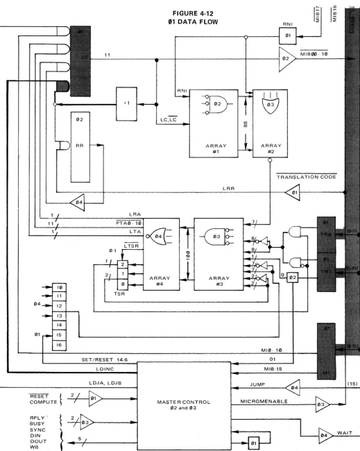
Figure 4-12 assumes, for the purposes of instruction, that the Location Counter is loaded from the incrementer. Concurrently, with the loading of the Location Counter at (/J 1, the Translation Register is also being loaded if either a L TR or an IW instruction was executed.
11
+1
02
RR
FIGURE 4-12 01 DATA FLOW
LC,LC
RNIr---~
ARRAY #1
I~
RNI
MIB!lJ0~ 10
I~
TRANSLATION CODE
01
RESET ~ 2 COMPUTE
RPLY'
~
BUSY SYNC
}
DIN
5
DOUT WB lACK
LRA
2
TSR
LDJA, LDJB
ARRAY #4
LRR
ARRAY #3
MASTE R CONTROL 02 and 03
4-10
JUMP
MI ROMENABLE
At the beginning of 02, (See Figure 4-13) the contents of the Location Counter are clocked out to the M I B bus (M I BOO -10) and to Array # 1. Both the true and complemented forms of the Location Counter are input to Array # 1. Also input is the RN I I ine. Array # 1 takes the input data word and de-termines whether or not it has a match. If it has a match, then the appropriate output is set at the end 0 f (/)2. I f there is no match, the translation proceeds no farther because no outputs are set.
I'll
LC
1'l2
RR
LRA
TSR
- }
RESET COMPUTERPLY
\
BUSY SYNC
ARRAY
#4
LRR
ARRAY
#3
MASTER CONTROL 1'l2 and 1'l3
I I I
\5J
TRANSLATION CODE
I'll
I'll
MI
(15)
DIN
}
WAITDOUT 5
WB lACK
FIGURE 4-13
At the beginning of 03, (See Figure 4-14), Array #2 samples the outputs from Array # 1 and d'"ter-mines whether any are active. If there is a match, then the translation code is generated and fed to Array #3, also during 03.
01
LC 11
02
RR
04
01
LDJA, LDJB
RESET }
2COMPUTE ---1---1
RPLY BUSY SYNC DIN DOUT WB lACK
+1
LRA
RNIr---~
LC,LC
0<3=
ARRAY #4
ARRAY #1
LRR
MASTER CONTROL 02 and 03
FIGURE 4-14
f1)3 DATA FLOW
4-12
I;
I~
RNI
MIBOO - 10
TRANSLATION CODE
01
TR0
01
TR1
01
MI
'I!)
G G
ill ~
( 15)
During 03, the contents of the selected byte of the Translation Register are fed to Array #3 along with the contents of the interrupt register, the Translation State Register, and the Q bit. During the later portions of 03, Array #3 determines if there is a match and, if a match is found, at the end of 03 an output is generated.
This output is fed into Array #4 at the beginning of 0 4. (See Figure 4-15). During 04, Array #4 de-termines whether there is an active input to it. If there is an active input, the contents of the word associated with the input are sent out at the end of 04. The Array #4 word mayor may not cau~e
the Translation State Register to be loaded, and mayor may not cause the Location Counter to be loaded at the next occurance of 0 1.
01
ARRAY #1
LRR
ARRAY
#3
I I I
~
ARRAY #2
RNI
I~
I~
MIBI!i0 ~ 10
TRANSLATION CODE
01
01
MI
~
G G
CD
~
(15)
- -
RESET}
COMPUTE RPLY BUSY SYNC DIN DOUT WB lACKMASTER CONTROL 02 and 03
FIGURE 4-15
~4 DATA FLOW
4-13
SECTION V
MICRO INSTRUCTIONS 5.1 INSTRUCTION REPERTOIRE
This section contains descriptions of the microinstructions. With each description is a diagram showing the format of the instruction and its operation code, given in hexadecimal. Above each diagram is the instruction mnemonic operation code, the argument needed by the assembler, and the name of the instruction. Under each diagram is a description of the command and its timing in clock cycles. It should be noted that the descriptions of the instructions are rather perfunctory. For a more thorough description of the instructions from a programmer's standpoint, the user is invited to review the MCP1600 MICRO PROGRAMMER's MANUAL.
The purpose of this section then is to outline the structure of the instruction set as an aid to under-standing the events on the two processor busses.
While the formats presented here describe 16 bits of the instruction word, be aware that the word is, in fact, 22 bits wide. The portion of the instruction described here control the operation of the processor. The other 6 bits are:
bits 16 and 17 are involved with control of the Location Counter. Bit 16 determines whether or not the contents of the Return Register will be loaded into the Location Counter. Bit 17 determines whether or not a Read Next Instruction translation will be invoked.
These two options are available on all instructions.
bits 18 through 21 have nothing to do with control of the MCP1600 system. They are available for the user to program as TTL levels. These bits are available on all instructions.
5.2 INSTRUCTION TYPES
All of the MCP1600 microinstructions are 22 bits long. Of the 22 bits, the 16 least significant effect the operation of the CPU. The purposes of the other 6 bits are covered in either the Programmed Translation Array description or the Micro I nstruction Bus description.
The instructions for the MCP1600 are divided into four classes as follows:
JUMP FORMAT
OP
I
RI
Address15 121110 0
This format provides an 11-bit Control ROM address. It causes an unconditional jump to any location in the permissable MICROM address space by always asserting the jump control line (JXX on the Data Chip or MIB 15 on the Micro Instruction Bus). The unconditional jump instruction is the only one that utilizes this format.
Unconditional jump instructions always take two clock cycles; one to decode the instruction, the second to load the Location Counter on the Control Chip.
A special case of this format is the Return From Subroutine instruction, covered later.
CONDITIONAL JUMP FORMAT
OP C ADDRESS
15 12 11
8 7
o
decodc; logic on the Delta Chip during the first cycle. This decision is communicated to the Control Chip via MI815 (.JXX on the Data Chip). During the second cycle the jump is affected.
LITERAL FORMAT
Literal
a
11=) 1211 43
o
Till, TUlll1dt provides 8-bit literal data. The "a" field usually specifies a I ile register. These instructions
II '" the 'literal path' to fetch data around the register file for the 'b' input to the ALU. All of
[lkS(1 !lhtrllctlOI1S execute in one clock cycle.
RH~!SnR FORMAT
~
________~
___ b ______ - L _ _ _ _ _a
____
~
15
8 7
43o
This furtll;.]t !:, by far Hw predominant one. In it, 'b' and 'a' are register file designators. Generally, df'pendln9 [JpOf) the operation, there can be two meanings to the register designators:
..
'b' (operation) 'a'
as, iOl irlstance, in a shift or move instruction
'b' (operation) 'a' 'a'
as, for installce, in an arithmetic instructioll.
'b' and 'a' can specify either a single byte data quantum or a word (double byte) data quantum. In thiS latter case, the designators usually point to the even addressed member of a register pair. While they rnay both point to an odd addressed pair, note carefully the instructions description for the effect.
I f the designators apply to a word data quantum, the instruction takes two cycles to execute. The following sections describe MCP1600 instructions by classes of function.
5.3 MCP 1600 MICRO·INSTRUCTION SET
The following rnicro-instructions are contained in the MCP 1600. The symbology used is listed in the table below.
Symbols
-..
( )
/\ V
.v-Rx Ry Ril
Rb Flag SeW ng
X (1)
Meaning
is transferred to
contents of location or register Logic Product (AN D)
Inclusive "or" Exclusive "or"
Forms extended register Ry
=
LSB, Rx=
MSBThe register specified by the micro-instruction "a" field
The register specified by the micro-instruction "b" field Designates no category
Don't care condition Flag cleared (set to 0) Flag set
Flag not affected
Set according to function (see flag description in Section 5.3.2)
5.3.1 TABLE OF MICRO-INSTRUCTIONS
Instruction OP Code Mnemonic Microcycles Description of Operation
Jump 0(0) JMP 2 (MI R10-00)·(LC) Jump unconditionally
to microm location specified by MI R10-00
Return from Subroutine 0(1) RFS 2 (R R ).( LC) Restore return address
from subroutines
Jump if lB False 10 J~BF 2 If ZS =0, (MIR 07-00HLC7-0) jump
conditionally within microm page
Jump if -rB True 11 HBT 2 If-rB=l, (MIR07-00)·(LC7-0)
Jump if C8 False 12 JC8F 2 If C8=0, (MI R07-(0).(LC7-0)
Jump if C8 True 13 JC8T 2 If C8=1, (M I R07-(0)·( LC7 -0)
Jump if I CS False 14 JIF 2 If ICS=0, (MIRQl7-00)·(LC7-0)
Jump if ICS True 15 JIT 2 If ICS=l, (MI R07-(0)·(LC7-0)
Jump if NB False 16 JNBF 2 If NB=Ql, (MIR07-00).(LC7-0)
Jump if NB True 17 JNBT 2 If N B-1, (M I R07 -(0).( LC7 -0)
Jump if -r False 18 J~F 2 If ~=Ql, (MI R07-00)·(LC7-0)
Jump if -r True 19 HT 2 If ~=1, (MI R07-00HLC7-0)
Jump if C False 1A JCF 2 If C=Ql, (MIR07-00)·(LC7-0)
Jump if C True 1B JCT 2 If C=l, (MIR07-00)·(LC7-0)
Jump if V False 1C JVF 2 If V=Ql, (MI R07-(0)·(LC7-0)
Jump if V True
10
JVT 2 If V=l, (MI R07-(0)·(LC7-0)Jump if N False 1E JNF 2 If N=Ql, (MIR07-00)·(LC7-0)
Jump if N True 1F JNT 2 If N=l, (MIR07-00)·(LC7-0)
Add Literal 2 AL (Ra)+Literal·Ra the 8 bit constant
is added to Ra
Compare Literal 3 CL (Ra)-Literal. The 8 bit result of the
I iteral is compared against Ra and the approprate flags set.
And Literal 4 NL (Ra)/\ Literal·(Ra) The 8 bit result
of a logical product of Ra and the literal are coded into Ra.
Test Literal 5 TL (Ra) /\ Literal The 8 bit result of the
logical product of Ra and the literal set condition Flags. The contents of Ra are unaffected.
Load Literal 6 LL Literal.(Ra). The 8 bit literal is
loaded into Ra.
Reset Interrupts 70 RI The three software interrupts 14, 15, and
16 are reset as indicated in the instruction's b field.
Set Interrupts 71 SI The three software interrupts 14, 15, and 16
are set as indicated in the instruction's b field.
Copy Condition Flags 72 CCF FlagS+(Ra) The four condition flags and
four ALU status flags are loaded in Ra
Load Condition Flags 73 LCF (Ra).Flags. The contents of Ra are
transferred to the AL U status flags unconditionally and to the condition flags under control of the b field.
Reset TSR 74 RTSR 0.(TSR). The three TSR bits in the
control chip are reset.
Load GLow 75 LGL (Ra) 2-0 .(G). The three least significant
bits of Ra are loaded into the G register.
Conditionally Increment 76 CIB If C8 is set, (Ra)+1 -(Ra)
Byte
Conditionally Decrement 77 COB If C8 is set, (Ra)-I - (Ra)
Instruction
OP
Code Mnemonic Microcycles Description of OperationMove Byte 80/81 MB (Rb)+(Ra). The 8 bit contents of Rb
are transferred to Ra. Rb is unaffected.
Move Word 82/83 MW 2 (Rb)+(Ra). The 16 bit contents ofRb+l: Rb
are transferred to Ra+1: Ra. Rb+1 and Rb are unaffected.
Conditionally Move Byte 84/85 CMB (Rb)+( Ra), if C=I. The 8 bit contents of
Rb are transferred to Ra if the carry flag is set from a previous operation.
Conditionally Move Word 86/87 CMW 2 (Rb)+(Ra), if C=I. The 16 bit contents of Rb+l: Rb are transferred into Ra+l: Ra if the carry flag is set from a previous operation. Shift Left Byte with Carry 88/89 SLBC (Rbm)+(Ram+I), (carry) +(Ra<,6). The 8
bit contents of Rb are shifted left one bit and loaded into Ra. The contents of the carry flag is inserted into the vacated low position of Ra.
Shift Left Word with Carry 8A/8B SLWC 2 (Rbm)+(Ram+I), (carry)+(Ra<,6). The 16 bit contents of Rb+l: Rb are shifted left one bit and loaded into Ra+l: Ra. The contents of the carry flag is inserted into the vacated low position of Ra.
Shift Left Byte 8C/80 SLB (Rbm)+(Ram+l) The 8 bit contents of
Rb are shifted left one bit and loaded into Ra.
I ncrement Byte by 1 90/91 ICBI (Rb)+I+(Ra). The 8 bit contents of Rb are
incremented by one and the result is transferred to Ra.
, I ncrement Word by 1 92/93 ICWI 2 (Rb)+I+(Ra). The 16 bit contents of Rb+I:Rb are incremented by one and the result transferred to Ra+l: Ra.
I ncrement Byte by 2 94/95 ICB2 (Rb)+2+(Ra). The 8 bit contents of Rb are
incremented by two and the result transferred to R a.
I ncrement Word by 2 96/97