820
INFORMATION PROCESSOR SOFTW ARE DEVELOPMENT GUIDE
Copyright© 1982 Xerox Corporation. All rights reserved.
Xerox Corporation 13111 West Mockingbird Lane
Dallas, Texas 752117
WARNING: This equipment has been certified to comply with the limits for a Class B computing device, pursuant to Subpart J of part 15 of FCC Rules. Only peripherals (computer input/output devices, terminals, printers, etc.) certified to comply with the Class B limits may be attached to this computer. Operation with non-certified peripherals is likely to result in interference to radio and TV reception.
WARNING: This equipment generates and uses radio frequency energy and if not installed and used properly, that is, in strict accordance with the manufacturer's instructions, may cause interference to radio and television reception. It has been type tested and found to comply with the limits for a Class B computing device in accordance with the specifications in Subpart J of part 15 of FCC Rules, which are designed to provide reasonable protection against such interference in a residential installation. However, there is no guarantee that interference will not occur in a particular installation. If this equipment does cause interference to radio or television reception, which can be determined by turning the equipment off and on, the user is encouraged to try to correct the interference by one or more of the following measures:
Reorient the receiving antenna.
Relocate the computer with respect to the receiver. Move the computer away from the receiver.
Plug the computer into a different outlet so that computer and receiver are on different branch circuits.
If necessary, the user should consult the dealer or an experienced radio/television technician for additional suggestions. The user may find the following booklet prepared by the Federal Communications Commission helpful.
"HOW TO IDENTIFY AND RESOLVE RADIO-TV INTERFERENCE PROBLEMS"
This booklet is available from the U.S. GOVERNMENT PRINTING OFFICE, WASHINGTON, D.C. 201102, STOCK NO. 0011-000-003115-11.
Xerox Corporation reserves the right to make improvements to products without incurring any obligation to incorporate such improvements in products previously sold.
Zilog and Z80 are trademarks of Zilog, Inc., with whom the publisher is not associated. Xerox® and 820™are trademarks of Xerox Corporation.
TABLE OF CONTENTS 820
SOFTWARE DEVELOPMENT GUIDE
INTRODUCTION
HARDWARE CPU BOARD
Microprocessor Memory
Floppy Disk Controller CRT Controller Par aile I Ports Serial Ports Real Time Clock Connector Pin-Outs Connector Location
KEYBOARD Keyboard Layout Keyboard Codes
POWER SUPPLY
Specifications
DISK FORMAT
CRT
Specifications
SOFTWARE MONITOR
Introduction Command Summary External Program Interface
INTERRUPT PROCESSING
Storage Location For Mode 2 Interrupt Table Device Priority List
iii
2-3 2-3 2-3 2-3 2-3 2-4 2-4 2-5 2-8
2-9 2-9
2-10
2-11
2-13
3-3 3-3 3-3 3-7
MEMORY Il,APPED CRT Operational Summary Screen Control Codes Programming Examples Display Character Codes
SYSTEM PORT NUMBERS
SERIAL PORTS Baud Rate Generator
PARALLEL PORTS
TIMER
REAL TIME CLOCK
CBIOS MODIFICATION PROCEDURE
MEMORY ORGANIZATION Memory Map
PROGRAM LISTINGS
MONITOR ROM VERSION 1.0 (U64 + U63) MONITOR ROM VERSION 2.0 (U64) MONITOR ROM VERSION 2.0 (U63) 5.25" CBIOS VERSION 2.0 8.00" CBIOS VERSION 2.0
ZILOG DATA Z80 CPU Z80 PIO Z80 CTC Z80 SIO
iv
3-10 3-10 3-11 3-13
3-14
3-15 3-17
3-18
3-21
3-24
3-29
3-31
4-3 4-34 4-59 4-71 4-80
THEORY OF OPERATION CENTRAL PROCESSOR CRT DISPLAY GENERATOR 64K RAM AND BANK SWITCHING
FLOPPY DISK CONTROLLER, SYSTEM PIO AND CTC GENERAL PURPOSE PIO AND 280 SIO
SCHEMATICS
POWER DISTRIBUTION (ETCH -1) PROCESSOR (ETCH -1)
CRT DISPLAY GENERATOR (ETCH -1) RAM (ETCH -1)
FLOPPY CONTROLLER, KEYBOARD INPUT, CTC (ETCH -1) GP, PIO, SIO (ETCH - 1)
POWER DISTRIBUTION (ETCH -2) PROCESSOR (ETCH - 2)
CRT DISPLAY GENERATOR (ETCH - 2) RAM (ETCH - 2)
FLOPPY CONTROLLER, KEYBOARD INPUT, CTC (ETCH - 2) GP, PIO, SIO (ETCH - 2)
v
6-3 6-4 6-6 6-7 6-8
7-3 7-4 7-5 7-6 7-7 7-8
INTRODUCTION
This is the 820 Software Development Guide. This guide contains the information needed to develop programs for the 820 IP and is not intended to teach you how to program.
HARDWARE
HARDWARE
The circuit board that is lying flat under the CRT is the CPU (central processing unit) board. [t contains the Z80 microprocessor, the memory and the [/0 devices. Reference is made throughout this document to etch I and etch 2 CPU boards. The boards can be identified by the following numbers etched on the board: An ETCH I board is 140P82629A and an ETCH 2 board is 140P82664A.
MICROPROCESSOR
The microprocessor for the Xerox 820 Information Processsor is a Zilog Z80 microprocessor. The processor clock speed is 2.5 Mhz. The Z80 microprocessor is automatically reset at power on or can be manually reset by pressing the reset button on the rear of the display.
MEMORY
The CPU board has 64K of RAM (program memory), 4K of ROM memory (system monitor) and 4K of Ram (CRT memory). The first 16K of system memory can contain either the first 16K of Ram (program memory) or the 4K of ROM memory (system monitor) and 4K of RAM (CRT memory).
When power is applied or the reset switch is depressed the monitor ROM / CRT RAM bank is enabled by hardware and the contents of the monitor ROM are moved by the Z80 microprocessor to the program memory starting at location FOOO (hex). When the move is complete the Z80 microprocessor transfers control to location FOOO (hex). The only other time that the monitor ROM / CRT RAM bank is enabled is when a character is sent to the screen. When the monitor ROM / CRT RAM bank is enabled the monitor ROM occupies memory at 0000 - OFFF (hex) and the CRT RAM occupies memory at 3000 - 3FFF (hex). User application programs need not be concerned with the bank switching as it is handled by the monitor and is transparent to transient programs.
FLOPPY DISK CONTROLLER
The CPU board is equipped with a Western Digital 1771 single density floppy disk controller. The clock rate for the 1771 is 2 Mhz. when an 8" disk is connected and 1 Mhz. when a 5.25" disk is connected. When an 8" disk is connected an external data seperator is used, when a 5.25" disk is connected the internal data seperator is used. This switching is controlled by the signal on the disk interface named 8/N5. [t will be a logic 1 when an 8" disk is connected and a logic 0 when a 5.25" disk is connected.
CRT CONTROLLER
The CPU board is equipped with a built in 80 character by 24 line CRT display controller. The refresh memory for the CR T is bank switchable from the systems 64K byte memory space. The Xerox 820 monitor ROM contains a CRT output driver routine that emulates the characteristics of the Lear Seigler ADM-3A. Many application packages require the terminal type to be specified, if the 820 is not listed as one of the options select the ADM-3A.
PARALLEL PORTS
The Xerox 820 Information Processor has two 8 bit parallel system ports and two 8 bit parallel general purpose ports. The A side of the system Z80 PIO is used for generation of the disc drive select signals, memory bank switching, disc drive identification and disc drive side select. The B side of the system Z80 P[O is used for the parallel keyboard input. The monitor contains an interrupt driven input handler for the keyboard that maintains a 16 character deep F[FO buffer for input data. This makes it possible to do a considerable amount of typing ahead without any characters being lost. If characters are typed while disk ac:cess is going on, they may be lost because the disk routines lock out all lower priority interrupts. Any characters received when the F[FO is full will also be lost.
The two general purpose 8 bit ports are unused by the system and can be connected to external parallel devices.
SERIAL PORTS
The Z80 510 supports two fuJI channels of serial I/O with the capability of supporting full RS-232 protocol on both channels. In addition, the A side of the 510 can provide clocks to synchronous modems or receive clocks from the modem.
Channel A of the Z80 510 can be configured to interface to a modem or a terminal. Refer to the Connector Pin-Outs for 39 and the schematic diagram (sheet 6).
Channel B of the Z80 510 is dedicated for printer operation and has no strapping options.
REAL TIME CLOCK
The CPU board has a Z80 CTC device that can be used as a timebase for interrupt driven timers, real-time clocks, and other time keeping functions. Channels 2 and 3 are used by the monitor to interrupt the processor once a second. Channel I is used by the monitor to perform disk index timing. Channel 0 is not initialized and can be used for other purposes.
CRT CONTROLLER
FLOPPY DISK CONTROLLER
MICROPROCESSOR
HARDWARE 2-4
REAL TIME CLOCK CONTROLLER
MEMORY
CONNECTOR PIN-OUTS
DISK CONNECTOR
Jl PIN ASSIGNMENT
2 8/5'A. Select
II Index
5 Select I
6 Select 2
7 Side
8 HDLD
9 Step In
10 Step
II Write Data
12 Write
13 TRK 00
III Write Protect
15 Read Data
16 Low Current
17 Ready
18 + 12 Volts
19 + 5 Volts
20-37 Ground
KEYBOARD CONNECTOR
J2 PIN ASSIGNMENT
I BIT 0
2 BIT 1
3 BIT 2
II BIT 3
5 BIT II
6 BIT 5
7 BIT 6
8 BIT 7
9 STROBE
13 +5 volts
111-25 Ground
PRINTER CONNECTOR
J3 PIN ASSIGNMENT
1 Ground
2 Receive Data (Input to 820)
3 Transmit Data (Output from 820)
II Clear to Send
5 Request to Send
6 Data Set Ready
7 Ground
8 Data Terminal Ready
20 Data Carrier Detect
MODEM CONNECTOR
J4 PIN ASSIGNMENT
1 Ground
2 Transmit Data
3 Receive Data
If Request to Send
5 Clear to Send
6 Data Set Ready
7 Ground
8 Carr ier Detect
15 Transmit Clock
17 Receive Clock
20 Data Terminal Ready
J5 PIN ASSIGNMENT
1 - 12 Volts
2 + 12 Volts
3 + 12 Volts
If Ground
5 Ground
6 Ground
7 + 12 Volts
8 + 5 Volts
9 + 5 Volts
J7 PIN ASSIGNMENT
3 Vertical Sync
If Hor izontal Sync
5 Video
6-10 Ground
8 BIT GENERAL PURPOSE PARALLEL PORT CONNECTOR
J8 PIN ASSIGNMENT
2 port A STROBE
If port A READY
6 port A bit 0
8 port A bit I
10 port A bit 2·
12 port A bit 3
Ilf port A bit If
16 port A bit 5
18 port A bit 6
20 port A bit 7
22 port BREADY
21f port B STROBE
26 port B bit 0
28 port B bit I
30 port B bit 2
32 port B bit 3
31f port B bit If
36 port B bit 5
38 port B bit 6
If 0 port B bit 7
odd II
pins Ground (ETCH 112 CPU only)
MODEM PORT OPTION (TERMINAL)
J9 PINS ASSIGNMENT
5 6 (M) TXD to Pin 3
7---8* (T) TXD to Pin 2
9 10 (M) RXD from Pin 2
11----12* (T) RXD from Pin 3 13 14 (M) RTS to Pin 5 15----16* (T) RTS to Pin 4 17 18 (M) CTS from Pin 4 19----20* (T) CTS from Pin 5 21 22 (M) DTR to Pin 8 23----24* . (T) DTR to Pin 20
25 26 (M) DCD from Pin 20
27----28* (T) DCD from Pin 8
29 30 Clock supplied to Modem as RX Clock 31----32* Clock supplied to SIO with RX Clock
33 34 Modem supplies 510 with RX Clock
35----36* Clock supplied to 510 with TX Clock 37 38 Modem supplies 510 with TX Clock 39 40 Clock supplied to Modem with TX Clock * 820 factory settings.
NOTE: (M) Indicates modem (data communications equipment) function. (T) Indicates terminal (data terminal equipment) function. For instance, exercising the (Tl strap option will allow communication with a modem. Exercising the (M) strap option would allow communicatiom with a terminal.
COUNTER/TIMER OPTION (TERMINAL) JIO
System Clock ZC/TOO ZC/TOI ZC/T02
*
820 factory settings.PIN 2 4----3* 6 5 8----7*
CLOCK/TRIGGER 0 CLOCK/TRIGGER I CLOCK/TRIGGER 2
CLOCK/TRIGGER 3
GENERAL PURPOSE PARALLEL PORT OPTION (TERMINAL)
J11 PIN ASSIGNMENT
3 4 port B READY polarity
5 6 port B lower direction
7 8 port A READY polarity
9 10 port A upper direction
11 12 port B upper direction
13 14 port A STROBE polarity
15 16 port B STROBE polarity
17 18 port A lower direction
all odd It pins are gounded
Refer to Parallel Ports in the Software section of this manual for a description of these jumpers.
J5 J2 J3
&20 INFORMA nON PROCESSOR CONNECTOR LOCATION
HARDWARE
2-&
ITl~@]0~~[]~~[!2][D]~@][ill
[ill~@]~~
;0; tTl[]QJ@]~§~~~~~~@g@]trl
~~~@]~
-<
t:P"n-lZ 0
g-l:ro
OO~~§]~~~~~~~~
50
~~@]~~
>
s·?=:-tri
:0(l) (!) ••
~~~~@]@]~@]~~@§l[]O
@]~§][?]~
0n+'<
oog;!
[EJI
74
I
[ill
~ ~[~
a-
iii" S'&.
g:.
fg-g
~ KEY NAME KEY 1/ UNSHIFTEDSHIFTED CONTROL KEY NAME KEY 1/ UNSHIFTEDSHIFTED CONTROLUi'C:::~
g@g(t
HELP 01 IE IE 9E"""'I.?-~' a. I 02 31 21 91 A 39 61 41 01
""nr+:J1lI 2 03 32 40 92 S 40 73 53 13
:r" cr
9(1) 1-.0 3 04 33 23 93 D 41 64 44 04
~ ~~ti
4 05 34 24 94 F 42 66 46 06y,< :r III 5 06 35 25 95 G 43 67 47 07
cr"" 6 07 36 5E 96 H 44 68 48 08
~
g
3 " 7 08 37 26 97 J 45 6A 4A OA~2.~
8 09 38 2A 98 K 46 6B 4B OBN :0 9 10 39 28 99 L 47 6C 4C OC
,
0 =E ... ", 0 11 30 29 90 SEMICOLON 48 3B 3A 7E'"
III!!E~ ~
MINUS 12 2D 5F IF APOSTROPHE 49 27 22 60>
0 ' " e: EQUAL 13 3D 2B 9A RETURN 50 OD OD 8D:0 C~e. BACKSPACE 14 08 08 88 LINEFEED 51 OA OA 8A
tTl
.gcn:r
DELETE 15 7F 7F FF UP ARROW 52 01 01 81e: cr" -(PAD) 16 2D 2D AD I (PAD) 53 31 31 BI
r+ 1-"><
...
7 (PAD) 17 37 37 B7 2 (PAD) 54 32 32 B2
'TI",n
"'"oR
8 (PAD) 18 38 38 B8 3 (PAD) 55 33 33 B3~ ...
"
9 (PAD) 19 39 39 B9 ( SHIFT 56 FUNCTION KEY:r",'" TAB 20 09 09 89 z 57 7A 5A IA
~ ==""Q Q 21 71 51 11 X 58 78 58 18
~no W 22 77 57 17 C 59 63 43 03
cr:ro. E 23 65 45 05 V 60 76 56 16
e: '" e: R 24 72 52 12 B 61 62 42 02
... .,n
g:.~~
T 25 74 54 14 N 62 6E 4E OEY 26 79 59 19 M 63 6D 4D OD
""cr U 27 75 55 15 COMMA 64 2C 3C IC
A~'<
~g~
I 28 69 49 09 PERIOD 65 2E 3E 7C0 29 6F 4F OF SLASH 66 2F 3F 5C
g~A P 30 70 50 10 R. SHIFT 67 FUNCTION KEY
.,
"
r
31 5B 7B IB L. ARROW 68 04 04 84o..>E!~ ] 32 5D 7D ID D.ARROW 69 02 02 82
... :r 0 ESC 33 IB IB 9B R.ARROW 70 03 03 83
"" '"
+ (PAD) 34 2B 2B AB o (PAD) 71 30 30 BO-0".,
S-1lIP- 4 (PAD) 35 34 34 B4 • (PAD) 72 2E 2E AE
5 (PAD) 36 35 35 B5 L. CTRL 73 FUNCTION KEY
6 (PAD) 37 36 36 B6 SPACE BAR 74 20 20 00
POWER SUPPLY
INPUT SPECIFICATIONS AC Voltage
The power supply is capable of operating from the following voltage and frequency ranges:
90 to 132 volts AC RMS or 198 to 26~ volts AC RMS jumper selectable, ~7 - 63 HZ
Electrical parameters are specified for 90 to 132 volts AC RMS, 60 HZ operation unless otherwise specified. Output requirements shall be met for the entire input voltage and frequency range.
INPUT CURRENT
The input current will not exceed 2.0 amps RMS. At turn-on, the peak inrush current will not exceed 35 amps at 115V RMS at room temperature of 25:!:50C.
INPUT CONNECTION/OUTPUT CONNECTION
PIN NUMBER SIGNAL NAME
Jl 1 AC Neutral
3 AC Hot
2 Void
P2 1 -12VDC
2 +12VDC III
3 +12VDC III
~ DC Ground
5 DC Ground
6 DC Ground
7 +12VDC 112
8 +5VDC
9 +5VDC
OUTPUT SPECIFICA nONS
MIN. CONTINUOUS PEAK
OUTPUT LOAD LOAD CURRENT LOAD CURRENT
DC VOLTS CURRENT
+5 2.0
III + 12 0.50
-12 0.25
112 + 12 0.50
MAXIMUM
~.65
]. 80 0.50 2.0
HARDWARE 2 - 10
MAXIMUM
~.65
2.8 0.5 2.0
RIPPLE TOLERANCE
P-P MV %
MAX. MAXIMUM
50 +2
50 +5
50 +5
Over Voltage Protection
The + 5.0VDC output shall be overvoltage protected. The over voltage protection circuitry shall be set to operate when the voltage output is between 120 and 11j0% of rated voltage.
Fuse Replacement FI (2.5 amp normal blow)
DISK FORMAT
The XEROX 820 Informaton Processor is equipped with two (2) Shugart SA400L (5",") drives, two Shugart SA800 (8") drives, or two Shugart SA450 (5",") drives.
A format is divided into three (3) parts, field A, field B, and field C. Field A is written at the start of each track known as the preamble. Field B is written once for each sector which consists of a gap between sectors, ID fields, and a data field. Field C is written at the end of each track and is known as a postamble.
The XEROX 820 Information Processor disks are initialized in the following formats:
PARAMETER 8"SSSD 5"'''SSSD 5"'''DSSD
Tracks 77 40 40
Sectors 26 18 18
Bytes/Sector 128 128 128
if of Reserved Track for OS 2 3 Y
Disk Capacity 241K 81K 172
Sides I 1 2
5"''' Format
Number of Hex Value Comment
Bytes of Bytes
Field A- 16 FF Preamble on Gap 4A
4 00 Gap 3
I FE ID Address Mark
I XX Track II
1 00
1 XX Sector II
I 00
*Field B 1 F7 Generate CRC
11 FF Gap 2
6 00
1 FB Data Address Mark
128 E5 Data Field 'E5' Data
1 F7 Generate CRC
& FF Gap &
Field C- 101 FF Postamble Gap 4B
* Repeated for number of sectors per track.
DISK FORMAT (continued)
8" Format
Number of Hex Value Comment
Bytes of Bytes
Field A- 28 FF Preamble - Write at the
6 00 start of each track
I Fe
26 FF
6 00 Gap 3
I FE ID Address Mark
I
XX
Track IfI 00
I
XX
Sector IfI 00
*Field B I F7 Generate CRC
11 FF Gap 2
6 00
I FB Data Address Mark
128 E5 Data Field '5' Data
I F7 Generate CRC
27 FF Gap 3
Field C- 247 FF Postamble Gap 4B
* Repeated for number of sectors per track.
CRT
SPECIFICATIONS Power
The CR T monitor shall function within the limits specified herein when the following power is supplied.
Phosphor
Resolution
Voltage: +12.0:!:5.0% VDC at 2.0 A DC maximum.
Ripple: 50 MV P-P synchronous or non synchronous with refresh or power frequency.
TYPE Aluminized Fluorescence Phosphorescence Persistence
P~
White (W) White (W) Short
With a 2~0 active line raster adjusted to 8.5 X 5.3 inches usable area and a brightness level of 37:!:2 foot-lamberts (bright screen - no characters), the resolution shall be as specified below. This specification shall be verified by supplying a synchronized video square wave signal to the unit and viewing the resultant screen image. Waveform duty cycle shall be 0.5:!: 10%. Signal frequency shall be 8.12 MHZ minimum. Individual black or white bars shall be visible with the unaided eye at a distance of 12 inches from the CRT faceplate. Optical magnification may be used only for dimensional and quantitative measurements.
VERT SYNC
HORIZ SYNC
Resolution at centers (within I" dia. circle) - 100 lines/in min.
SIGNAL TIMING
u
HARDWARE
Video bit rate (time) 10.694 MBPS (93.51 nS) Active bits per
horizontal line (time) 560 (52.366 uS)
Horizontal line
blanking bits (time 140 (j3.091 uS)
Horizontal front
porch-bits (time) 0
Hor izontal sync
pulse-bits (time 140 03.091 uS)
Hor izontal back
porch-bits (time) 0
Total bits per line (time) 700 (65.457 uS)
Horizontal rate 15.278 KHZ
Active lines per field (time) 240 05.710 mS)
Vertical blanking lines (time) 20 (1.309 mS)
Vertical front
porch-bits (time 0
Vertical sync pulse-bits (time) 20 (1.309 mS)
Vertical back porch-bits (time) 0
Vertical retrace (Jines) 8 TYP.
Total lines per field 260
Field rate (time) 58.758 Hz (17.019 mS)
Ineut Signal Descr ietion
Horizontal Vertical
Parameter Video Sync Sync
Input Type Single Single Single
Ended Ended Ended
Z In R Shunt 150 :': 5% RShunt =2K Minimum
CShunt 30 pf max CShunt = 50 pf max
Amplitude Low = 0 = 0 to + 0.4V Low = 0 = 0 to 0.4 V
Polarity
Rate
Rise/Fall Times 10% to 90%
High = 1 = 2.5 :': 0.1 V High = I = 2.0 to 5.0V
I = Brite
o
= Dark10.69 Mbps Max Less than
20 nsec
I = Sync
15,278 Hz:': 100Hz
Less than 100 nsec
HARDWARE
2 - 14
o
= SyncBrite
-300V Max
-DC
-SOFTWARE
SOFTWARE MONITOR
INTRODUCTION
The XEROX &20 system monitor is the basic control program for the single-board computer. It begins execution when the computer is first turned on, or whenever the reset button is pressed, and resides in the top 4K of RAM memory (FOOO-FFFF).
The monitor provides two essential functions for the system. It is the initial software level of the computer and it contains the routines that initialize and control all the basic system input/output resources. The "front panel" functions of the monitor include commands to display and alter the contents of memory and I/O ports, to begin execution at a given address, enter typewriter mode, and to bootstrap programs from disk. The basic I/O functions of monitor provide driving routines for the built-in CRT display and keyboard input, and the floppy disk controller. In this capacity the monitor is always active, even when application programs like the CP/M disk operating system have control of the CPU.
The following sections of this manual will explain how to use the console monitor commands, what facilities are provided by the resident I/O handlers, and how to interface applications programs to the monitor.
COMMAND SUMMARY
The Xerox &20 monitor enters the command mode after it has initialized the system following a power-on or a reset. The following sign-on message is displayed on the console output device as an indication that the monitor is ready to accept commands •
••. XEROX &20 .•. Enter A for BOOT Enter T for TYPEWRITER
*
Commands consist of a single character command name and zero to three hexadecimal numeric parameters separated by commas or spaces. The command line may be entered using upper case or lower case letters. A carriage return is used as the terminator. Errors within a line can be corrected by typing backspace to delete the last character. If a line is ent~red with an unknown command name, an invalid number or parameters or an out-of-range parameter, an error message will be displayed and the command will not be executed.
The user may wish to halt long running commands like the memory dump before they are finished. This can be done by typing carriage return while the command is doing output. Output can also be frozen temporarily and then re-started by typing repeatedly on the space bar.
The following table summarizes the monitor's command set. The items enclosed in angle brackets represent the numeric parameters expected by the command. A detailed description of each command is provided in the following pages.
Command d(ump) m(emory) x(test) fOil) c(opy) g(oto) r(ead) a(boot) t(ypewriter) i(nput) o(utput)
D (start), (end) M (address) X (start), (end)
F (start), (end), (constant)
C (source start), (source end), (dest start)
G (addresS) -
-R (unit), (track), (sector) A(boot)
T I (port)
o
(port), (data)NOTE: All of the Monitor parameters are in hexadecimal.
DUMP COMMAND (D)
The dump command outputs a tabular display of the contents of memory in hexadecimal and ASqI representation. Each display line has the following format:
aaaa dd dd dd dd dd dd dd dd dd dd dd dd dd dd dd dd cccccccccccccccc
where aaaa is the starting memory address of the line in hexadecimal, the dd's are the hex values of the 16 bytes of data starting at location aaaa, and the c's are the ASCII characters equivalent to each data byte. Bytes less than 20 hex are replaced in the ASCII portion of the dump by period.
The dump command accepts zero, one or two address parameters. If two addresses are specified, the block of memory between those two locations will be dispayed. Entering only one address will display 256 bytes of memory starting at the specified location. Typing 'D' with no parameters will cause the routine to display the 256 byte block of memory starting at the last address displayed by the dump command.
MEMORY COMMAND (M)
The memory examine/change command allows the contents of individual memory locations to be read from and written into using the monitor. This command accepts one parameter representing the memory address at which to begin examining data. The display format is as follows:
AAAA DD
where AAAA is the current memory address and DD is the hexadecimal value of the data in that location. After displaying the contents of a memory location, the routine waits for one of the following items to be input from the console.
• Typing a carriage return will cause the routine to display the data at the next memory location, with no modification of content.
• Typing a minus sign will have a similar effect, except the address is decremented instead of incremented.
• Typing a two digit hexadecimal number will cause that number to be stored at the displayed address. The new data is stored as soon as the second digit is entered, with no terminating character required.
• Typing any character other than carriage return, a minus sign or a hexadecimal digit will cause the command to terminate.
TEST COMMAND (X)
This command allows the user to test memory for errors. Any portion of memory may be tested except the area reserved for the monitor (FOOO to FFFF hex). Two parameters are required from the user; the starting address and ending address of the memory block to be tested. Only the high order 8 bits of the addresses entered are actually used. If no errors occur, the test routine will output a plus sign every time a test pass is done. A total of 256 plus signs must be output for all possible test patterns to have been tried. When errors are detected an error line will be output in the following format:
AAAA DD should=XX
where AAAA is the address of a location that fails to test, DD is the data read back from the location, and XX is the test pattern that was written there.
FILL COMMAND (F)
The fill command allows blocks 'of memory to be filled with a fixed data constant. Three parameters are required in the command line; a starting memory address, an ending address and a fill constant. Each location in the specified block of memory has the constant written into it and then read back again to check for memory errors. An error line like the one described for the 'X' command is printed for any locations that fail to verify.
SOFTWARE
COPY COMMAND (C)
The copy command allows blocks of data to be moved around in memory. Three parameters are required in the command line; a starting memory address, an ending address, and a destination address. The contents of the block of memory bounded by the first two addresses is copied to the block starting at the third address. As with the fill command, a test is made to verify that each byte of the destination block, when read back, is the same as the corresponding byte in source block.
GO TO COMMAND (G)
The goto command allows control of the CPU to be passed to another program by the monitor. This command requires a single parameter from the user representing the address at which to begin execution. The monitor actually passes control to the specified location by executing a CALL instruction. This makes it possible for the external routine to return to the monitor by doing a RET, assuming it does not re-Ioad the stack pointer and loose the return address to the monitor.
READ COMMAND (R)
The read command allows individual disk sectors to be read into memory and displayed on the console. Three parameters are required; a drive unit number (range 0 to 1), a track number (range 0 to 27 for 5.25" disks or range 0 to 4D for 8" disks) and a sector number (range I to 12 for 5.25" disks or range 1 to lA for 8" disks). The command routine performs a drive select, track seek and sector read sequence using the supplied parameters. If no errors occur, the contents of the input buffer will be dumped out the 'D' command format. In the event of a disk error, a diagnostic message will be printed in the following format:
disk error XX UAA TBB SCC
where XX represents the 1771 disk controller error status code, AA is the unit number, BB is the track number, and CC is the sector number. The error code is composed of eight bits of status information as described in the table below:
bit read/write seek/restore/select
7 drive not ready drive not ready
6 write protected unused
5 write fault unused
4 record not found seek error
3 ere error crc error
2 lost data cannot restore
I unused unused
0 always=l always=O
The least significant bit (LSB) of the error code indicates which of the above sets of error conditions is applicable. If the LSB= 1 the disk error was generated by a read or write operation, otherwise it was caused by a seek, restore, or select operation.
BOOT COMMAND (A)
The boot command command is used to load and begin execution of a one sector long bootstra. loader from drive unit zero. The most common use of this command will be to boot up the CP/M disk operating system, although it is not necessarily restricted to this purpose only. The boot works by reading the contents of track 0, sector I into memory at location 80 hex anc the jumping to that address to start execution of the code just read in. Normally the routine or sector I will be a small loader that in turn reads in a larger program such as the operatin~
system.
SOFTWARE
TYPEWRITER COMMAND (T)
This command allows the XEROX 820 to be used as a standard electronic typewriter. All key strokes will be typed directly on the 630 printer in a direct print mode, without displaying any typed information on the screen.
INPUT COMMAND (I)
This command allows the contents of input ports to be read from using the monitor. It operates very much like the memory examine command, except that input ports are being examined instead of memory locations. A single parameter representing a port number is expected in the command line. The contents of adjacent ports can then be examined by typing carriage return or a minus sign as in the 'M' command. Typing any other key will cause the routine to terminate.
OUTPUT COMMAND (0)
The output command is provided to allow output ports to be written to using the monitor. Two parameters are expected in the command line; a port number and a data byte to be output to that port. Both parameters should be between 0 and FF hex. After outputting the specified data to the port, this routine simply returns to the monitor instead of stepping to the next location like the input command. This makes it possible to use the output command to initialize Z-80 peripheral devices like the SIO, PIO and CTC.
EXTERNAL PROGRAM INTERFACE
This section gives the locations and calling sequences of the user accessible I/O routines in the XEROX 820 monitor.
XEROX 820 subroutines are accessed via a table of JUMP instructions beginning at memory location FOOO hex. All monitor calls should be made to these entry points, since the actual addresses of the routines inside XEROX 820 will vary between different releases. Parameter passing conventions for the monitor fall into one of two groups. The character oriented I/O routines all pass data using the A register, while the disk routines pass parameters in C and HL and return status information in A.
Storage for the monitor's stack and working variable occupies the top 256 bytes of memory, from FFOO to FFFF hex. The mode 2 interrupt vector table takes up the first 32 bytes of this block.
XEROX 820 SUBROUTINE ENTRY POINTS
LOCATION FUNCTION PARAMETERS FOOO INIT • . . IN: none
F003
F006
F009
FOOC FOOF
FOl2
FOl5
"FOI8
FOIB
F01E
OUT:does not return
PROMPT . . . IN: none
OUT:does not return CONST • .. IN: none
OUT:status in A
CONIN • •• IN: none
OUT:character in A
CRTOUT.. IN: character in A OUT:none SIOST.. IN: none
OUT:status in A
SIOIN . • . IN: none
OUT:character in A
SIOOUT . .• IN: character in A OUT:none
SELECT ••• IN: unit number in C
**
OUT:status in AHOME. .. IN: none
**
OUT:status in ADESCRIPTION
Perform cold start initialization of XEROX 820 monitor and enter command mode.
Enter XEROX 820 monitor command mode with no initialization Test for data ready in console input FIFO and return status in A. If data is available then A=FF hex, else A=OO. Return character from console input FIF in A. If FIFO is empty then loop until character is input.
Output character passed in A to the memory-mapped CRT display. Test for received data available from SIO channel B and return status in A. If data is available then A=FF hex, else A=OO.
Return received data from SIO channel E in A. Loop until data is received if none is available on entry.
Output charater passed in A to SIO channel B transmit register. Select specified drive for future restore, seek, read or write command. If the drive is not ready, then the currently selected drive is left on. Move read/write head to home position at track 0 and verify if it got there. F021 SEEK . . . IN: track number in C Move read/write head to specified track
**
OUT:status in A and verify if it got there.EXTERNAL PROGRAM INTERACE (continued)
LOCATION FUNCTION PARAMETERS DESCRIPTION
F02li READ. • . IN: sector number in C Read specified sector on current track buffer pointer in HL into memory data buffer.
**
OUT:status in AF027 WRITE. .• IN: sector number in C Write specified sector on current track buffer pointer in HL from memory data buffer.
**
OUT:status in A*
Inoperative on level 2.0 ROM**
If the status returned in the A register is 00 the function was performed with no errors. Error conditions returned a the A register are as follows:bit read/write see k/ restore / sel ect
7 drive not ready drive not ready
6 write protected unused
5 write fault unused
If record not found seek error
3 crc error ere error
2 lost data cannot restore
I unused unused
0 always=1 always=O
The least significant bit (LSB) of the error code indicates which of the above sets of error conditions is applicable. If the LSB=I the disk error was generated by a read or write operation, otherwise it was caused by a seek, restore, or select operation.
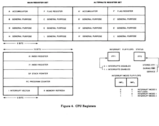
INTERRUPT PROCESSING
The XEROX 820 monitor takes advantage of the powerful interrupt handling capabilities of the Z80 microprocessor. Interrupts are utilized in the
I/o
drivers for the console keyboard input, the real-time dock and the floppy disk controller. All necessary initialization tasks and interrupt service routines for these devices are contained in the monitor.For the most part, the operation of the interrupt mechanism should be transparent to applications programs that will run on the XEROX 820. A few precautions must be taken however, to insure that user written software does not adversely effect the operation of the system. The following list describes the major hazards to the interrupt system;
Interrupts should not be disabled permanently by user code, as this will lock-up the console input and real-time-dock routines.
The Z80 'I' register should never be altered.
The CPU operates in Z80 interrupt mode 2 and should not be switched to either of the other two interrupt modes.
Adequate stack space must be reserved in user programs to allow at least one level of stack f or interrupt return addresses.
The monitor initializes the Z80 'I' register to point to the system interrupt vector table at location FFOO to FFIF hex. This table contains pre-assigned vector locations for all the peripheral devices on the XEROX 820.
STORAGE ALLOCATION FOR MODE 2 INTERRUPT TABLE
FFOO SIOVO: DEFS2 ;Z80 SIO port B xmit buffer empty FF02 SIOVI: DEFS2 ;Z80 SIO port B external/status change FF04 SIOV2: DEFS2 ;Z80 SIO port B receive data available FF06 SlaV): DEFS2 ;Z80 SIO port B special receive condition FF08 SIOV4: DEFS2 ;Z80 SIO port A xmit buffer empty FFOA SIOV5: DEFS2 ;Z80 SIO port A external/status change FFOC SIOV6: DEFS2 ;Z80 SIO port A receive data available FFOE SlaV?: DEFS2 ;Z80 SIO port A special receive condition FFIO CTCVO: DEFS 2 ;Z80 CTC channel 0 interrupt
FFI2* CTCVI: DEFS2 ;Z80 CTC channel I interrupt FFI4* CTCV2: DEFS2 ;Z80 CTC channel 2 interrupt FFI6* CTCV): DEFS2 ;Z80 CTC channel ) interrupt FFI8 SYSVA: DEFS2 ;system Z80 Pia port A interrupt FFIA* SYSVB: DEFS2 ;system Z80 Pia port B interrupt FFIC GENVA: DEFS2 ;general purpose Z80 Pia port A interrupt FFIE GENVB: DEFS 2 ;general purpose Z80 Pia port B interrupt * Vectors used by the Monitor ROM (Version 1.0 & 2.0)
DEVICE PRIORITY LIST
The Interrupt Priority chain is organized high to low as follows:
Z80 SIO CHANNEL A Z80 SIO CHANNEL B SYSTEM Z80 Pia PORT A SYSTEM Z80 Pia PORT B
GENERAL PURPOSE Z80 Pia PORT A GENERAL PURPOSE Z80 Pia PORT B Z80 CTC CHANNEL 0
Z80 CTC CHANNEL 1 Z80 CTC CHANNEL 2 Z80 CTC CHANNEL)
MEMORY MAPPED CRT
CRT DRIVER OPERATIONAL SUMMARY
All character codes between 32 (20 hex) and 127 (7F hex) are directly displayable on the screen.
All character codes between 00 and 31 (IF hex) are interpreted as control characters. Only 12 of these codes have an effect on the CRT display, and are described in the table below. The remaining 20 are treated as nulls.
New characters are stored on the screen at the location occupied by the cursor. The cursor is then moved one space to the right.
If the cursor is positioned at a screen location occupied by a non-blank character, the presence of the cursor will be indicated by making the overlaid character blink.
If a linefeed (LF) is output when the cursor is on the bottom line of the screen, the entire display is scrolled up one line and a new blank line is created on the bottom.
If the displayed character is output when the cursor is in the right most column of the screen, an automatic carriage return and linefeed is generated.
820 SCREEN CONTROL CODES
DECIMAL CODE
08 09 10
II
12 13 17 21t 26 27 30 31
HEX CODE
08 09
OA
OB
OC
OD
II18 IA IB IE IF
ASCII NAME
BS HT LF VT FF CR DCI CAN SUB ESC RS VS
SOFTWARE 3 - 10
CRT-EFFECT
Cursor Left (backspace) Horizontal Tab Cursor Down (linefeed) Cursor Up
Cursor Right Carr iage Return Clear to end of screen Clear to end of line Clear screen
Initiate escape sequence Home cursor
PROGRAMMING EXAMPLES
Cursor Left
Moves the cursor to the left one column. If the cursor is in the left most column of the screen, this character has no effect.
Horizontal Tab
Example in Basic to move the cursor one space to the left: 100 PRINT CHR$(8);
liD END
Moves the cursor right to the next tab stop. The tab stops are fixed at every eighth column, starting from the left.
Example in Basic to move the cursor to the right 3 tab stops: 100 FOR X = I TO 3
120 PRINT CHR$(9); 130 NEXT X JIIO END Cursor Down (!inefeed)
Moves the cursor down one line on the screen. If the cursor is at the bottom most line, the screen is scrolled up and a blank line is created on the bottom. The top line is lost.
Cursor Up
Example in Basic to move the cursor down 5 lines: 100 FOR X = I to 5
110 PRINT CHR$(lO); 120 NEXT X 130 END
Moves the cursor up one line on the screen. If the cursor is on the top of the screen it rolls around to the bottom.
Cursor Right
Example in basic to move the cursor up 5 lines: 100 FOR X = I to 5
liD PRINT CHR$(ll); 120 NEXT X 130 END
Moves the cursor to the next column to the right. If the cursor is in the right most column, there is no effect.
Carr ier Return
Example in Basic to move the cursor 5 spaces to the right: 100 FOR X = I to 5
110 PRINT CHR$(l2); 120 NEXT X 130 END
Moves the cursor to the left most column of the screen.
Example in Basic to move the cursor to the left column: 100 PRINT CHR$(l3);
110 END
SOFTWARE
Clear to End of Screen
Clears the contents of the screen from the current cursor position to the end of the bottom line.
Example in Basic to Clear to the end of the screen: 100 PRINT CHR$O 7);
110 END Clear to End of Line
Clears the contents of the line the cursor is on, from the cursor position to the end of the line.
Clear Screen
Example in Basic to Clear to the end of the line: 100 PRINT CHR$(24l;
110 END
Clears the entire screen regardless of the current cursor position and places the cursor in the top left corner of the screen.
Example in Basic to clear the screen: 100 PRINT CHR$(26); Escape Sequence
Used to initiate an XY cursor positioning sequence. The cursor can be moved to an arbitrary location on the screen by outputting a 4 character sequence composed of: J) ESCAPE -CHR$(27), 2) EQUALS sign - CHR$(61), 3) ROW /I (0-23) + 32, 4) COLUMN /I (0-79) + 32.
Home Cursor
Example in Basic to clear the screen and position the cursor on Row 10, Column 40 and print an X.
100 PRINT CHR$(26);
120 PRINT CHR$(27l;CHR$(61);CHR$(J0+32);CHR$(40+32); 130 PRINT 'X';
140 END
Moves the cursor to the top left corner of the screen, without altering any characters on the display.
Example in Basic to home the cursor: 100 PRINT CHR$(30); 110 END
Display Special Character
Functions as a prefix character to force the output of special symbols in the character generator. This character must precede any character in the display code chart from 00 thru IF (hex).
For example, to display the vertical bar character (code 19 hex on the display code chart), the following basic program could be used:
100 PRINT CHR$(3J); 110 PRINT CHR$(25); 120 END
D1SPLA Y CHARACTER CODES
This table shows the code for each character to be displayed by the XEROX 820. Each character is defined by a unique eight bit code which is represented by a hexadecimal code 'XV' where X represents the 4 most significant bits of the code and Y represents the 4 least significant bits of the code.
There are a total of 128 characters in the font set. Therefore, Y represents a hexadecimal number from
0
to F, and X represents a hexadecimal number from lito 7. Therefore, the complete font set is defined by codes from00
to 7F.If the most significar)t bit of the eight bit code is set to 'I', then the complete font set is duplicated with the blink attribute set. The blinking set of characters is then defined by codes from 811 to FF (Level 2.0 ROM only).
2 4 5 6 7 8 9 A B C D E F
'/J
0
¢•
§
12
~t
+I 1- "- ~ t- ~ @...
3 Z 0
~
'R
!
I..l
t
+' +'
@ ~It-2 II
$
% &*
+3
0
2 3 4 5 6 7 8 9 ?4 @ A B C D E F G H J K L M N 0
5 P Q R S T U V W X Y Z
C
\ ]6 a b c d e g h k m n 0
7 P q u v w x y Z fm
SYSTEM PORT NUMBERS
PORT 00 = CHANNEL A BAUD RATE (WRITE ONLY) PORT 04 = Z80 SIO CHANNEL A DATA
PORT 06 = Z80 SIO CHANNEL A CONTROL
PORT OC = CHANNEL B BAUD RATE (WRITE ONLY) PORT 05 = Z80 SIO CHANNEL B DATA
PORT 07 = Z80 SIO CHANNEL B CONTImL
PORT 08 = GENERAL PURPOSE Z80 PIO PORT A DATA PORT 09 = GENERAL PURPOSE Z80 PIO PORT A CONTROL PORT OA = GENERAL PURPOSE Z80 PIO PORT B DATA PORT OB = GENERAL PURPOSE Z80 PIO PORT B CONTROL
PORT 10 = 1771 STATUS/COMMAND REGISTER PORT 11 = 1771 TRACK REGISTER
PORT 12 = 1771 SECTOR REGISTER PORT 13 = 1771 DATA REGISTER
PORT 14 = CRT SCROLL REGISTER (WRITE ONLY)
PORT 18 = Z80 CTC CHANNEL 0 PORT 19 - Z80 CTC CHANNEL 1 PORT lA = Z80 CTC CHANNEL 2 PORT IB = Z80 CTC CHANNEL 3
PORT lC = SYSTEM Z80 PIO PORT A DATA PORT ID = SYSTEM Z80 PIO PORT A CONTROL PORT IE = SYSTEM Z80 PIO PORT B DATA (KEYBOARD) PORT IF = SYSTEM Z80 PIO PORT B CONTROL (KEYBOARD)
SERIAL PORTS
A 280 SIO provides the 820 with a serial interface to the outside world. The 280 SIO has two Channels, A & B. The printer port is Channel B and the modem port is Channel A. Channel B is initialized by the ROM MONITOR, Channel A is uninitialized.
The monitor initializes Channel B as follows: SIO-Register*
4
I
3 5 2
DATA (Hex) COMMENTS 45
04 41 2A 00
16X Clock, I Stop Bit, Odd Parity Status affects Vector
RX-7 Bits/Character, Rx-enable TX-7 Bits/Character, Tx-enable, RTS Base Interrupt Vector
Channel B Baud Rate is set to 300 baud by the monitor, and to 1200 baud when the CP/M disk is loaded.
The software supplied by XEROX uses ETX/ACK protocol to "handshake" with the printer. This handshaking is done in the CBIOS and can be changed to use other methods of handshaking. Let's assume that we have a serial printer that has a Logic TRUE (high) on pin 20 when it is ready to receive a character. When it cannot receive another character Pin 20 will be low for busy. The software to accomplish this follows:
;
:List device output routine, assume character is in the C register. ;Handshake with the printer using Pin 20 on the interface.
;
;Note: Pin 20 is connected to the DCD pin on the SIO.
;
;Constants - For 280 SIO Channel B
;
SIOBCO SIOBDA SIORES RDYMSK
;
LSTOUT:
EQU EQU EQU EQU
LD OUT IN AND CP
JR
LD OUT RET
07 05 10H OOOOIlOOB
A,SIORES (SIOBCO),A A,(SIOBCO) RDYMSK RDYMSK N2,LSTOUT A,C (SIOBDA),A
CHANNEL A INITIALI2A TION
;SIO Channel B Control ;SIO Channel B Data Port
;SIO Reset External Status Command ;Mask to check for SIO and Printer Ready
;Get External Reset Command to A Register ;Send to Channel B Control Port
;Read Channel B Control Port ;Mask of Everything of Interest ;Check for Expected Result ;Repeat until Everything is Ready ;Get Character to A Register ;Send to Data Port
;Return to Caller
Channel A is not initialized, before using Channel A you should set-up the desired operating mode. As an example, the following sub-routine could be used to initialize Channel A.
;
;Channel A 280 SIO Initialization Routine
;
CONST ANTS FOR SIO Channel A
;
SIOACO SIOADA BAUDA XMTRDY RCVRDY
EQU EQU EQU EQU EQU
06 04 00 OOOOOIOOB OOOOOOOIB
;Channel A 280 SIO Control Port ;Channel A 280 SIO Data Port ;Channel A Baud Rate Port ;Transmit Buffer Ready Bit ;Receive Character Ready Bit LD C,SIOACO ;Get Port Number to C Register
OVRTBL:
STABL:
LD LD OTIR LD OUT RET
B,6 HL,STABL A,05 (BAUDA),A
DEFB Oli
DEFB 01000100B DEFB 03 DEFB OIOOOOOIB DEFB 05 DEFB 10101010B
;Byte Count to Register B
;Point H & L Register to the Start of the table ;Do output and Increment
;Set A Register for 300 Baud ;Set Channel A Baud Rate
;Select Register !lli
;16X Clock, I Stop Bit, No Parity ;Select Register 113
;7 Bits/RX Character, RX-enable ;Select Register !l5
;7 Bits/TX Character, DTR active, TX-enable The following routines will do input, output and status checking on Channel A:
;
;CHAOUT - Subroutine to output the charater in the C Register to Channel A
;
CHAOUT: IN
AND JR LD OUT RET
A,(SIOACO) XMTRDY Z,CHAOUT A,C (SIOADA),A
;Read Channel A Control Port ;Check X-Mit Buffer Empty Flag ;Repeat until Ready
;Character to A Register ;Output Character ;Back to Caller
;CHASTA - Subroutine to check the receive status of Channel A A Register = 00 if no character is ready
;
CHASTA: IN
AND RET LD RET
A Register = FF if a character is ready A,(SIOACO)
RCVRDY
Z
A,OFFH
;Read Channel A Control Port ;Check Receive Character Available ;If Zero Return
;Put FF in A Register ;Back to Caller ;CHAINP - Subroutine to read a character from Channel A
;
CHAINP:
Return with the character in the A Register CALL CHASTA
JR Z,CHAINP
IN A,(SIOADA)
RET
;Get Receive Status ;Repeat until Character is r ;Get Character to A Register ;Back to Caller
BAUD RATE GENERATOR
The 820 provides the user with two programmable baud rate generators. Channel A baud rate resides at port 00 hex and is write only. Channel B baud rate resides at port OC hex and is also write only. The programming procedure is as follows:
Load the accumulator with the hex value for the desired BAUD rate (See table below). Output the contents the accumulator to the desired serial channel.
The following sub-routine would initialize Channel A for 9600 Baud and Channel B for 300 Baud.
LD OUT LD OUT RET
A,OEH (O),A A,05 (OCH),A
BAUD RATE TABLE 00 hex = 50 Baud 01 hex = 75 Baud 02 hex = 110 Baud 03 hex = 134.5 Baud 04 hex = 150 Baud 05 hex = 300 Baud 06 hex = 600 Baud 07 hex = 1200 Baud 08 hex = 1800 Baud 09 hex = 2000 Baud OA hex = 2400 Baud OB hex = 3600 Baud OC hex = 4800 Baud OD hex = 7200 Baud OE hex = 9600 Baud OF hex = 19.2 Kbaud
;Code for 9600 Baud to A Register ;Output to Channel A
;Code for 300 Baud to A Register ;Output to Channel B
PARALLEL PORTS
The 820 has two 280 PIO's on the CPU Board, one is dedicated for the systems' use, the other is available to the user and is called the General Purpose (GP) PIO. The Port assignments for the GP PIO are as follows:
PORT I! 08 09
OA
DB
Oeser iption
GP PIO PORT A DATA GP PIO PORT A CONTROL GP PIO PORT B DATA GP PIO PORT B CONTROL
Description of hardware jumpering options on the GP-PIO (JIJ):
Jl1
PINS DESCRIPTION9-10 Port A, Bit.7 through Bit I; Direction Control ON - Outputs from the 820
OFF - Inputs to the 820
17-18 Port A, Bit 3 through Bit 0 Direction Control ON - Outputs from the 820
OFF - Inputs to the 820 7-8 ARDY Pulse (PORTA)
ON - Non-inverted OFF - Inverted 13-11! ASTB Pulse (PORT A)
ON - Non-inverted OFF - Inverted
11-12 PORT B, Bit 7 through Bit I! Direction Control ON - Outputs from the 820
OFF - Inputs to the 820
5-6 PORT B, Bit 3 through Bit 0 Direction Control ON - Outputs from the 820
OFF - Inputs to the 820 3-1! BRDY Pulse (PORT B)
ON - Non-inverted OFF - Inverted 15-16 BSTB Pulse (PORT B)
ON - Non-inverted OFF - Inverted
The hardware jumpering on
ill
determines the direction select of the transceiver (7I!LS21!3) that is connected between the 280 PIO and J-8. The 280 PIO must also be set-up with software commands to select the direction of signal flow in the 280 PIO.PROGRAMMING EXAMPLE
Lets assume that you have a paper tape punch that you want to connect to the 820 through th~
Parallel Port. This punch has eight Data Bits And a strobe as its inputs from the 820. Th~
output of the punch is a ready signal which will be low when ready to receive characters. Th~
strobe will be software generated on bit 2 of the B side.
This sub-routine would have to be executed once to initialize the Z80 PIO.
GPACON EQU 09 jgeneral purpose PIO A control
GPADAT EQU 08 jgeneral purpose PIO A data
GPBCON EQU OBH jgeneral purpose PIO B control
GPBDAT EQU OAH jgeneral purpose PIO B data
INTPIO: LD C,GPACON jPort II to C register
LD B,3 jOutput 3 bytes
LD HL,GPPIO jPoint HL & I to table
OTIR jOutput & Increment HL
LD C,GPBCON jPort If to C again
LD B,3 jOutput 3 bytes
OTIR jOutput & Increment HL
LD A,OFH jStrobe starts off high
OUT (GPBDAT),A jSend to PIO B data
RET jreturn to main program
jPORT A
GPIO: DEFB 07 jDisable interrupts
DEFB OCFH jSet port A to mode 3
DEFB 00 jMake all eight bits 'outputs
jPORT B
DEFB 07 jDisable interrupts
DEFB OCFH jSet port B to mode 3
DEFB OFOH jBits 4-7 inputs, bits 0-3 outputs
This sub-routine will output the character in the C register to the paper tape punch.
PUNOUT: IN
AND
JR
LD OUT IN RES OUT SET OUT RET
A,(GPBDAT) IOH NZ,PUNOUT A,C (GPADAT),A A,(GPBDAT) 2,A (GPBDAT),A 2,A (GPBDAT),A
jread port B into A register jmask out all but ready jrepeat until Punch is ready jget character to A register jsend character to punch jread channel B to A register jmake strobe line low jmake strobe line high jback to calling routine
The paper tape punch would be connected to the Parallel Port as follows:
820 PUNCH
J8
PAO 6
~) DATA 0
PAl 8
»
DATA IPA2 10
~) DATA 2
PA3 12
~) DATA 3
PAIl ll!
»
DATAl!PA5 16
»
DATA 5PA6 18
~) DATA 6
PA7 20
»
DATA 7PB2 30
~) STROBE
PI;I! 31!
»
READY*GND odd II pins
»
GND*
On ETCH 1 CPU Board, pick up ground for J8 on odd pins of J I J.The following jumpers would be installed on JlI:
PINS FUNCTION
9-10 Select output for high nibble of Port .\ 17-18 Sel.ect output for low nibble of Port A
5-6 Select output for low nibble of Port B
SOFTWARE
TIMER
The Xerox 820 is equipped with a Z80 CTC (Counter Timer Circuit). The CTC has four independent channels that perform counting and timing functions. Channels I, 2 and 3 are used by the 820's monitor.
Channel 0 is not used and can be configured to perform counting or timing functions for your program.
The following example is when the CTC might be used and some programmng examples to help you understand its operation.
Lets assume that you are writing a program that among other things, samples an input signal that is connected to a temperature sensitive switch located on your manufacturing line. When this input goes to a logic I (+ 5 volts) you want the 820 to activate an alarm (also connected to the parallel port) by making an output signal a logic I (+ 5 volts), also you want to display a message on the 820's screen to inform the operator that there is a fire on the manufacturing line. Lets say that you have determined that this input needs to be looked at about 60 times each second.
A simple solution would be to use the Z80 CTC channel 0 and program it to give the 820 an interrupt every 16.69 milliseconds. Your interrupt service routine would look at the input and if it is a logic I (+ 5 volts) activate the alarm and display the message on the screen.
Lets assume that the input signal comes into the 820's General Purpose Port channel A on bit 7, and the alarm is connected to channel A on bit O. You would have to install a jumper on JIl between pins 17 and 18 to select bits 0 - 3 as outputs.
Listed below is an example of how to:
• Initialize the CTC as a timer to generate an interrupt signal every 16.69 milliseconds. • Write an interrupt service routine for the Z80 CTC.
• Disable the Z80 CTC's interrupt before exiting the program •
• Z80 CTCVEC GPACON GPADAT CTCO SENSOR ALARM BDOS WBOOT PRTSTG CLRSCN
;
EQU EQU EQU EQU EQU EQU EQU EQU EQU EQU
OFFIOH 09 08 18H 10000000B OOOOOOOIB 5
o
9 IAH
;CTCO VECTOR LOCATION IN TABLE ;GP PIO CHANNEL A CONTROL PORT ;GP PIO CHANNEL A DATA PORT ;CTC CHANNEL 0 PORT II ;SENSOR BIT
;ALARM BIT ;BDOS ENTRY POINT ;CP/M WARM ENTRY POINT jCP/M PRINT STRING FUNCTION ;820 CLEAR SCREEN CHARACTER
; YOU MUST EXECUTE THE "IN IT" ROUTINE BEFORE THE CTC-O WILL START ; GENERATING INTERRUPTS. TYPICALLY THIS WOULD BE BEFORE THE MAIN ; BODY OF YOUR PROGRAM.
CALL INIT ;GO INITIALIZE CTC-O &. GP PIO
;*****************************
*
MAIN PROGRAM
*
;
;*****************************
;
;---THE MAIN PART OF YOUR PROGRAM WOULD GO HERE.
SOFTWARE
;
;---IF YOUR PROGRAM NEEDS TO TERMINATE & GO BACK TO CP/M ;---IT SHOULD DO SO BY JUMPING TO THE EXIT ROUTINE. ;---THIS WILL DISABLE THE CTC-O INTERRUPTS
JP EXIT ;EXIT TO CP/M
;
; INITIALIZATION SUBROUTINE - THIS ROUTINE WILL BE EXECUTED ONCE AT ; THE BEGINNING OF YOUR PROGRAM.
;
; I - STORE INTERRUPT SER VICE ROUTINE ADDRESS IN THE MODE 2 INTERRUPT ; TABLE (FFIO).
; 2 - SET UP THE PIO TO MONITOR THE SENSOR AND CONTROL THE ALARM ; 3 - SET UP THE CTC CHANNEL 0 TO GENERATE AN INTERRUPT EVERY 16.69
MILLISECONDS.
INIT: LD
LD LD LD LD OTIR XOR OUT LD LD LD OTIR RET
HL,INTROU (CTCVEC),HL C,GPACON B,I+ HL,PIOTBL A
(GPADAT),A C,CTCO B,2 HL,CTCTBL
;PIO INITIALIZATION TABLE
PIOTBL: DEFB
DEFB DEFB DEFB
00 OCFH OFOH 07 ;CTC INITIALIZATION TABLE CTCTBL: DEFB 10 100 III B
DEFB 163
;
;INTERRUPT ROUTINE'S ADDRESS ;SAVE IN INTERRUPT TABLE ;GP PIO CHANNEL A CONTROL PORT ;OUTPUT FOUR BYTES
;START OF PIO TABLE ;SEND TABLE TO PIO ;A REGISTER = 00
;MAKE ALARM OUTPUT = 00 ;CTC CHANNEL 0 PORT II TO C ;OUTPUT TWO BYTES
;ST AR T OF CTC TABLE ;SEND TO CTC ;BACK TO CALLER
;DISABLE INTERRUPTS ;SET TO MODE 3 ;BIT 1+-7 = INPUT'S ;INTERRUPT SWITCH
;CTC 0 SET TO TIMER MODE ;CTC 0 PERIOD 163*256*1+00 NSEC.
; INTERRUPT SERVICE
ROUTINE-; THIS ROUTINE WILL BE EXECUTED ONCE EVERY 16.69 MILLISECONDS. ; IT WILL DO THE FOLLOWING:
; I - MONITOR SENSOR INPUT
; 2 -WHEN INPUT IS HIGH ACTIVATE ALARM AND DISPLAY MSG ON SCREEN.
INTROU: PUSH
PUSH PUSH PUSH IN AND JR LD OUT LD LD CALL JR
HL BC DE AF A,(GPADAT) SENSOR Z,NOTHOT A,ALARM (GPADAT),A C,PRTSTG DE,MESGI
BDOS '
OUT!
;SAVE REGISTERS
;READ GP PIO CHANNEL A DATA ;MASK ALL BUT SENSOR INPUT ;IF RESULT = 00 - NO FIRE ;ELSE SOUND ALARM ;ACTIVA TE ALARM ;PRINT STRING FUNCTION ;POINT TO MESSAGE ;EXIT INTERRUPT ROUTINE
MESGJ: DEFB CLRSCN
DEFM
' ***
FIRE ON MANUFACTURING LINE*** ,
DEFM'$'
NOTHOT: XOR A ;CLEAR A REGISTER
OUT (GPADAT),A ;TURN ALARM OFF
OUTl: POP AF ;RESTORE REGISTERS
POP DE
POP BC
POP HL
EI ;ENABLE INTERRUPTS
RETI ;RETURN FROM INTERRUPT
;
; ROUTINE THAT USER'S PROGRAM SHOULD JUMP TO WHEN IT IS READY ; TO EXIT BACK TO CP/M. THIS ROUTINE DISABLES THE CTCO INTERRUPT ; AND DOES A CP/M WARM BOOT.
EXIT: LD
DI OUT EI JP END
A,OI (CTCO),A
o
;PREPARE TO DISABLE CTC ;DISABLE INTERRUPTS ;SEND TO CTC-O ;INTERRUPTS OK NOW ;BACK TO CP/M
REAL TIME CLOCK
The following program is the 280 assembly listing for a Real Time Clock. This program can be entered assembled and run on your 820 without making any hardware modifications or additions. Features: 12 or 2L! hour format
Time can be displayed on the screen if desired
Memory locations that store the time can be accessed from other programs to read the current time.
NOTE: This clock increments the seconds every .999936 micro-seconds. This along with tolerances in the system master oscillator will effect the accuracy of the clock. Typically over a 2L! hour period it may gain or loose as much as 20 seconds.
You will need the following to create and assemble the program: Text Editor (such as, Xerox Word Processing) M80.COM (280 assembler on CP/M disk) L80.COM (Linker on CP/M disk)
First you will need to enter this program with a text editor and name the file CLOCK.MAC. If
you are using the Xerox Word Processing, choose the E command - edit a program from the directory menu. When the program has been entered, run the assembler by entering: M80 CLOCK,CLOCK=CLOCK. When the assembly process is complete you should get a message that there were no fatal errors. If you do not get this message, check your typing for errors. Next you will link your file by entering: L80 CLOCK,CLOCK/N/E. This will generate a file named CLOCK.COM on your disk.
You can now execute the clock program by entering: CLOCK (RET) This brings up a screen of instructions on what to enter to activate and set the clock. For example, if you entered CLOCK 50093000 the clock would be set for standard time, display the time on the screen and set the time for 9:30:00. If you enter clock after the program has been loaded, it will come back and tell you what memory locations the hours, minutes and seconds are stored at .
BOOS PRTSTG CLRSCN CR LF CTC3 BASEl BASE2 CLKORG HOURS MINUTE SEC NOS
,
. 280 EQU EQU EQU EQU EQU EQU EQU EQU EQU EQU EQU EQU
5 9 IAH ODH OAH OFF 16H OFF75H OFF78H OFEOOH OFF5CH HOURS + I
MINUTE +1
iBDOS ENTRY POINT
iCP/M PRINT STRING FUNCTION iCLEAR SCREEN CODE iCARRIAGE RETURN CODE iUNE FEED CODE
iCTC CHANNEL 3 INTERRUPT VECTOR iBASE VARIABLE (1.0 ROM)
iBASE VARIABLE (2.0 ROM) iORIGIN FOR CLOCK ROUTINE iHOURS VARIAB
iMINUTES VARIABLE LOCATION iSECONDS VARIABLE LOCATION
iFIRST CHECK FOR CLOCK MODULE ALREADY LOADED, IF IT IS DISPLAY iMESSAGE AND GO BACK TO CP/M
BEGIN: LD
CP JR LD LD CALL RST
A, (OFEOOH) OFFH 2,PROCED DE,RESET C,PRTSTG BOOS
o
iCHECK FOR CLOCK ALREADY LOADED iPROCEED IF NOT
iPOINT TO RESET MESSAGE iPRINT STRING FUNCTION TO C iCALL BOOS
iBACK TO C