17
Power Delay Analysis of Parallel Self-Timed Adder by
Recursive Approach
Kallepelli Srikanth
1, M. Swetha
2M.Tech. VLSI System Design1, Asst. Prof. ECE Dept.2, Vaagdevi College of Engineering, Warangal.1, 2 Email: [email protected]1, [email protected]2
Abstract-This paper presents a PArallel Self-Timed Adder (PASTA). It is based on recursive formulation and use only half adders for performing multi bit binary addition. Theoretically the operation is parallel for those bits that do not need any carry chain propagation. Thus the new approach attains logarithmic performance without any special speed-up circuitry or look-ahead schema. The corresponding CMOS implementation of the design along with completion detections unit is also presented. The design is regular and does not have any practical limitations of fan-ins or fan-outs or complex interconnections. Simulation have been performed using Tanner Tool and verify the practicality and superiority of the proposed approach over existing asynchronous adders.
Index Terms-Asynchronous circuits; Binary adders; CMOS design; Digital arithmetic.
1. INTRODUCTION
Binary addition is the single most important operation that a processor performs. In addition to explicit arithmetic (such ad addition, subtraction, multiplication, and division) performed in a program, additions are performed to increment program counters and calculate effective address [1]. The performance of processors is significantly influenced by the speed of their adders (it is shown by [2]). Statistics presented in [1], [2] show that, in a prototypical RISC machine (DLX), 72 percent of the instructions perform additions (or subtraction) in data path. It is even (reported by [3]) reaches to 80 percent in ARM processors.
The adders can be sequential or combinational. As the sequential adders are bound to perform slowly due to its incremental nature of operation it is not considered for parallel and fast adders. The Half-Adders (HA) are simplest single bit adders. The full-adders are single bit full-adders with the provision of carry input and output. The full-adders are typically composed of two HAs and hence are expensive than half-adders in terms of area, time and interconnection complexity. The most common approach for designing multi-bit adders is to form a chain of FA blocks by connecting the carry out bit of a FA to the carry in bit of the next FA block.
Circuits may be classified as synchronous or asynchronous. Synchronous circuits have a clock to synchronize the operations of subsystems, while asynchronous circuits do not. Most of the adders have been designed for synchronous circuits even though there is a string interest in clockless/asynchronous processors/circuits [4]. Asynchronous circuits do not assume any quantization of time. Therefore, they hold great potential for logic design as they are free from several problems of clocked (asynchronous) circuits.
In principle, logic flow in asynchronous circuits is controlled by a request-acknowledgment handshaking protocol to establish a pipeline in the absence of clocks. Explicit handshaking blocks for small elements, such as bit adders, are expensive. Therefore, it is implicitly and efficiently managed using dual-rail carry propagation in adders. A valid dual-rail carry output also provides acknowledgment from a single-bit adder block. Thus asynchronous adders are either based on full dual-rail encoding of all signals (more formally using null convention logic [5] that uses symbolically correct logic instead of Boolean logic) or pipelined operation using single-rail data encoding and dual-rail carry representation for acknowledgments. While these constructs add robustness to circuit designs, they also introduce significant overhead to the average case performance benefits of asynchronous adders. Therefore, a more efficient alternative approach is worthy of consideration that can address these problems.
Briefly, the embodiment of this invention is to provide a recursive formulation for PArallel Self-Timed Adder (PASTA) [6]. The design of PASTA is regular and uses Half Adders along with multiplexers with minimum interconnection requirement. Thus the interconnection and area requirement is linear making it easy to fabricate in VLSI chip. The design works in truly parallel manner for the number of bits that do not require carry propagation. Thus theoretically it can perform in logarithmic time as the carry chains for long number of bits are logarithmic and significantly smaller.
18 bit adder. Whenever a carry is generated or needs
propagation from a bit position, it is transferred to higher bit level and hence its own carry is modified to zero. Thus the construction of plurality of adders is pretty similar to RCA. The advantage is that it is self-time and logarithmic. It will signal the completion of addition as soon as all the carry signals from individual bit adders are zero.
The implementation in this brief is unique as it employs feedback through XOR logic gates to constitute a single-rail cyclic asynchronous sequential adder [7]. Cyclic circuits can be more resource efficient than their acyclic counterparts [8], [9]. On the other hand, wave pipelining (or maximal rate pipelining) is a technique that can apply pipelined inputs before the outputs are stabilized [10]. The proposed circuit manages automatic single-rail pipelining of the carry inputs separated by propagation and inertial delays of the gates in the circuit path. Thus, it is effectively a single-rail wave-pipelined approach and quite different from conventional pipelined adders using dual-rail encoding to implicitly present the pipelining of carry signals.
2. BACKGROUND
There are a myriad designs of binary adders and we focus here on asynchronous self-timed adder. Self-timed refers to logic circuits that depend on and/or engineer timing assumptions for the correct operation. Self-timed adders have the potential to run faster averaged for dynamic date, as early completion sensing can avoid the need for the worst case bundled delay mechanism of synchronous circuits. They can be further classified as follows.
2.1. Pipelined Adder Using Single-Rail Data Encoding
The asynchronous Req/Ack handshake can be used to enable the adder block as well as to establish the flow of carry signals. In most of the cases, a dual-rail carry convention is used for internal bitwise flow of carry outputs. These dual-rail signals can represent more than two logic values (invalid, 0, 1), and therefore can be used to generate bit-level acknowledgment when a bit operation is completed. Final completion is sensed when all bit Ack signals are received (high).
The Carry-Completion Sensing adder (CCSA) is an example of a pipelined adder [11], which uses full adder (FA) functional blocks adapted for dual-rail carry. A CCSA is regarded as an asynchronous version of an RCA. Instead of using clock pulses to synchronize adder operation, a CCSA uses some extra circuitry to implement the start and completion signal. On the other hand, a speculative completion adder is proposed in [12]. It uses so-called abort logic and
early completion to select the proper completion response from a number of fixed delay lines. However, the abort logic implementation is expensive due to high fan-in requirements.
2.2. Delay Insensitive Adder Using Dual-Rail Data Encoding
Delay Insensitive (DI) adders are asynchronous adders that assert bundling constraints or DI operations. Therefore, they can correctly operate in presence of bounded but unknown gate and wire delays [5].
Though dual-rail encoding doubles the wire complexity, they can still be used to produce circuits nearly as efficient as that of the single-rail variants using dynamic logic or nMOS only design. An example 40 transistors per bit DIRCA adder is presented in [11] while the conventional CMOS RCA uses 28 transistors.
Similar to CLA, the DICLA defines carry propagate, generate, and kill equations in terms of dual-rail encoding [11]. They do not connect the carry signals in a chain but rather organize them in a hierarchical tree. Thus, they can potentially operate faster when there is long carry chain.
A further optimization is provided from the observation that dual-rail encoding logic can benefit from settling of either the 0 or 1 path. Dual-rail logic need not wait for both paths to be evaluated. Thus, it is possible to further speed up the carry look-ahead circuitry to send carry-generate/carry-kill signals to any level in the tree. This is elaborated in [11] and Subsequently, it iterates using earlier generated carry and sums to perform half-additions repeatedly until all carry bits are consumed and settled at zero level.
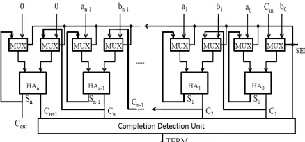
The general block diagram of the PArallel Self-Timed Adder (PASTA) is presented in Fig. 1. Multi-bit adders are often constructed from single Multi-bit adders using combinational and sequential circuits for asynchronous or synchronous design. The sequential circuits are often serial/chain adders and are not the match for high speed combination adder.
19 Fig. 1. General block diagram of Parallel Self-Timed
Adder
3.1. Single Bit Adder
Single bit Half-Adder (HA) and Full-Adder (FA) are the fundamental building block for nearly all high-speed adders. A single bit HA for ith bit addition is logically formulated as follows:
Si =ai⊕bi
Ci+1 = aibi Eq. (1) A single bit full adder implementation additionally takes consideration of the carry-in input from the preceding single bit unit and formulated as follows:
Si =ai⊕bi⊕ci
Ci+1 = aibi+( ai⊕bi) ci Eq. (2) The recursive binary addition formula for addition of two n-bit numbers as follows.
3.2. Recursive Formula for Binary addition
Let Sij and Ci+1j denote the sum and carry, respectively, for ith bit at the jth iteration. The initial condition (j=0) for addition is formulated as follows:
Si0=ai⊕bi
Ci+10= aibi . Eq. (3) The jth iteration for the recursive addition is formulated by
Sij = Sij-1⊕ Cij-1, 0 ≤ i < n Eq. (4)
Ci+1 j
= Si j
Ci j-1
, 0 ≤ i < n. Eq. (5) The recursion is terminated at kth iteration when
the following condition is met:
Cnk+Cn-1k+...+C1k=0,0≤k<n Eq. (6) Now the correctness of the recursive formulation is inductively proved as follows.
Observation 3.1. In a single bit adder with no carry
in, the maximum obtainable result is 2(=102).
Proof. It is obvious that the sum cannot exceed the maximum sum obtained by two highest possible operands and hence should be equal or less than 2(=102).
The significance of this observation is that for individual ith bit adder, the case of having Si=1 and
Ci+1 =1 (decimal value of 3) is impossible as it will exceed the maximum of sum of two input which is
2(binary 10). Thus the only valid (Si, Ci+1) forms by ith bit adder are (0, 0), (0,1) and (1,0).
Theorem 3.2. The recursive formulation of Eq.
(3)-Eq. (6) will produce correct sum for any number of bits and will terminate within a finite time.
Proof. We prove the correctness of the algorithm by induction on the required number of iteration for completing the addition (meeting the terminating condition).
Basis. Consider the operand choices for which no carry propagation is required, i.e. Ci0=0 for ∀i, i ∈ [0..n]. The proposed formulation will produce the correct result by a single-bit computation time and terminate instantly as Eq. (6) is met.
Induction. Assume that Ci+1k ≠ 0 for some ith bit at kth iteration. Let l be such a bit for which Cl+1k= 1. First we show that it will be killed in the (k + 1)th iteration and next we show that it will be successfully transmitted to next higher bit in the (k + 1)th iteration.
According to Observation 3.1, the kth iteration of
lth bit state (Ckl+1, Skl) and (l + 1)th bit state (Ckl+2, Skl+1) could be in any of (0, 0), (0, 1), or (1, 0) states. As
Ckl+1 = 1, it implies that Skl = 0. Hence, from (3),
Ck+1l+1 = 0 for any input condition between 0 to l bits. We now consider the (l + 1)th bit state (Ckl+2, Skl+1) for kth iteration. It could also be in any of (0, 0), (0, 1), or (1, 0) states. In (k+1)th iteration, the (0, 0) and (1, 0) states from the kth iteration will correctly produce output of (0, 1) following Eq. (4) and Eq. (5). For (0, 1) state, the carry successfully propagates through this bit level following Eq. (5).
Thus, all the single-bit adders will successfully kill or propagate the carries until all carries are zero fulfilling the terminating condition.
3.3. Architecture of PASTA
The general architecture of the adder is shown in Fig. 1. The selection input for two-input multiplexers corresponds to the Req handshake signal and will be a single 0 to 1 transition denoted by SEL. It will initially select the actual operands during SEL = 0 and will switch to feedback/carry paths for subsequent iterations using SEL = 1. The feedback path from the HAs enables the multiple iterations to continue until the completion when all carry signals will assume zero values (terminating condition is met).
3.4. State Diagrams
20 respectively, from the ith bit adder block. During the
initial phase, the circuit merely works as a combinational HA operating in fundamental mode. It is apparent that due to the use of HAs instead of FAs, state (11) cannot appear. During the iterative phase (SEL = 1), the feedback path through multiplexer block is activated. The carry transitions (Ci) are allowed as many times as needed to complete the recursion.
Fig. 2. State diagrams for PASTA. (a) Initial phase. (b) Iterative phase.
4. IMPLEMENTATION OF PARALLEL
SELT-TIMED ADDER (PASTA)
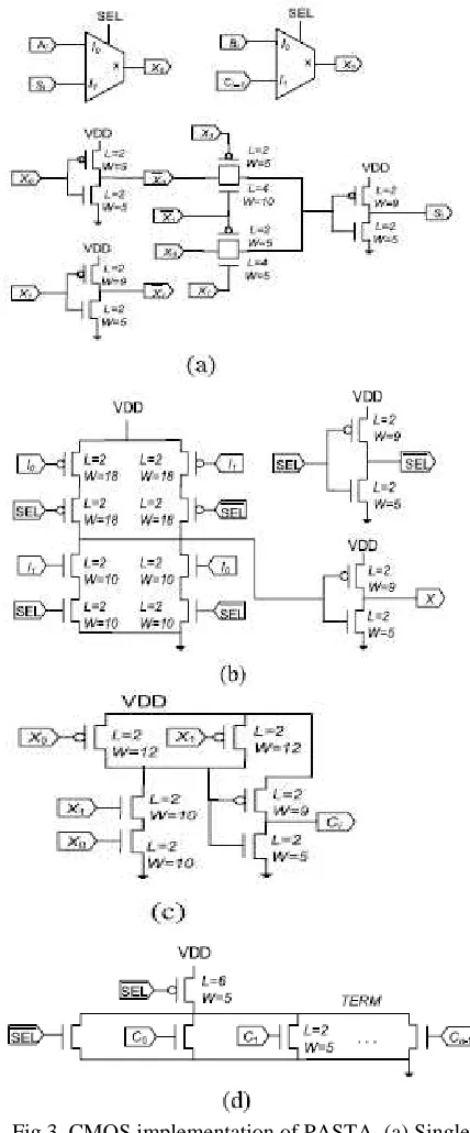
A CMOS implementation for the recursive circuit is shown in Fig. 3. For multiplexers and AND gates we have used TSMC library implementations while for the XOR gate we have used the faster ten transistor implementation based on transmission gate XOR to match the delay with AND gates [7]. The completion detection following Eq.(6) is negated to obtain an active high completion signal (TERM). This requires a large fan-in n-input NOR gate. Therefore, an alternative more practical pseudo-nMOS ratio-ed design is used. The resulting design is shown in Fig. 3(d). Using the pseudo-nMOS design, the completion unit avoids the high fan-in problem as all the connections are parallel. The pMOS transistor connected to VDD of this ratio-ed design acts as a load register, resulting in static current drain when some of the nMOS transistors are on simultaneously. In addition to the Ci s, the negative of SEL signal is also included for the TERM signal to ensure that the completion cannot be accidentally turned on during the initial selection phase of the actual inputs. It also prevents the pMOS pull up transistor from being always on. Hence, static current will only be flowing for the duration of the actual computation.
5. SIMULATION RESULTS
In this section, we present simulation results for different adders using Tanner Tool version 13.0. For
implementation of other adders, we have used standard library implementations of the basic gates. The custom adders such as DIRCA/DICLA are implemented based on their most efficient designs from [11].
Fig.3. CMOS implementation of PASTA. (a) Single-bit sum module. (b) 2×1 MUX for the 1 Single-bit adder. (c) Single-bit carry module. (d) Completion signal
detection circuit.
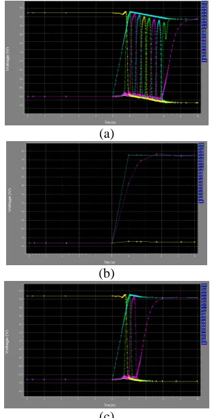
21 case for maximum, minimum and average length carry
propagation is highlighted in the timing diagrams of FIG. 4 (a), (b) and (c). In Fig. 4, the timing diagrams for worst and average cases corresponding to maximum and average length carry chain propagation over random input values are highlighted. The carry propagates through successive bit adders like a pulse as evident from Fig. 4(a). The best-case corresponding to minimum length carry chain does not involve any carry propagation, and hence incurs only a single-bit adder delay before producing the TERM signal. The worst-case involves maximum carry propagation cascaded delay due to the carry chain length of full 16 bit.
(a)
(b)
(c)
Fig.4. SPICE timing diagram for PASTA implementation using TSMC 0.25 µm process. (a) Worst-case carry propagation while adding operands
(FFFF)16 and (0101)16. (b) Best-case carry propagation while adding random operands of (F7F7)16 and (0000)16. (c) Average-case carry propagation while adding random operands of
(F7F7)16 and (0101)16.
The delay performances of different adders are shown in TABLE 1. We have used random operands to represent the average case while best case, worst case correspond to specific test cases representing zero, 32-bit carry propagation chains respectively. The delay for combinational adders is measured at 70% transition point for the result bit that experiences the maximum delay. For self-timed adders, it is measured
by the delay between SEL and TERM signals, as depicted in Fig. 4(a).
TABLE 1: Comparison of different 16-bit adders using TSMC 0.25 µm process with 5.0 volt input voltage(and supply voltage) in Tanner Tool v13.0 Type of
Adder
Worst Case Delay (ns)
Best Case Delay
(ns)
Average Case Delay (ns)
Average Power Dissipation
(mW) DIRCA 5.5 2.09 3.23 120.4
DICLA 3.9 2.19 3.03 286.3 CCSA 3.48 3.03 2.4 212.8
RCA 2.7 1.46 1.67 138.3 B-CLA 3.34 1.25 2.4 238.6
PASTA 2.8 0.3 1.39 108
PASTA performs best among the self-timed adders. PASTA performance is comparable with the best case performances of conventional adders. Effectively, it varies between one and four times that of the best adder performances. It is even shown to be the fastest for TSMC 0.25 µm process. For average cases, PASTA performance remains within two times to that of the best average case performances while for the worst case, it behaves similar to the RCA. Note that, PASTA completes the first iteration of the recursive formulation when “SEL = 0.” Therefore, the best case delay represents the delay required to generate the TERM signal only and of the order of picoseconds. The interesting observation is that the performances of the combinational adders and PASTA improve with the decreasing process width and VDD values while the performance of dual-rail adders decreases with scaling down of the technology [15].
The average power consumption of different adders for different operand choices (best, worst, and average carry chain lengths) are shown in TABLE 1. We measure average power consumed by combinational and self-timed adders for the duration of input pattern placement and completion of the addition. PASTA consumes least power among the self-timed adders.
6. CONCLUSION
22 unit for the proposed adder is also practical and
efficient. Simulation results are used to verify the advantages of the proposed approach.
REFERENCES
[1] J.L. Hennessy and D.A. Patterson, Computer Architecture: A Quantitative Approach. Morgan Kaufmann, 1990.
[2] M.A. Franklin and T. Pan, ªPerformance Comparison of Asynchronous Adders,º Proc. Int'l Symp. Advanced Research in Asynchronous Circuits and Systems, pp. 117-125, Nov. 1994. [3] J.D. Garside, ªA CMOS VLSI Implementation of
an Asynchronous ALU,º Asynchronous Design Methodologies, S. Furber and M. Edwards, eds., vol. A-28 of IFIP Trans., pp. 181-207 1993.. [4] D. Geer, “Is it time for clockless chips?
[Asynchronous processor chips],” IEEE Comput., vol. 38, no. 3, pp. 18–19, Mar. 2005.
[5] J. Sparsø and S. Furber, Principles of
Asynchronous Circuit Design. Boston, MA, USA:
Kluwer Academic, 2001.
[6] P. Choudhury, S. Sahoo, and M. Chakraborty, “Implementation of basic arithmetic operations using cellular automaton,” in Proc. ICIT, 2008, pp. 79–80.
[7] M. Z. Rahman and L. Kleeman, “A delay matched approach for the design of asynchronous sequential circuits,” Dept. Comput. Syst. Technol., Univ. Malaya, Kuala Lumpur, Malaysia, Tech. Rep. 05042013, 2013.
[8] M. D. Riedel, “Cyclic combinational circuits,” Ph.D. dissertation, Dept. Comput. Sci., California Inst. Technol., Pasadena, CA, USA, May 2004. [9] R. F. Tinder, Asynchronous Sequential Machine
Design and Analysis: A Comprehensive
Development of the Design and Analysis of Clock-Independent State Machines and Systems. San
Mateo, CA, USA: Morgan, 2009.
[10]W. Liu, C. T. Gray, D. Fan, and W. J. Farlow, “A 250-MHz wave pipelined adder in 2-µm CMOS,”
IEEE J. Solid-State Circuits, vol. 29, no. 9, pp.
1117–1128, Sep. 1994.
[11]F.-C. Cheng, S. H. Unger, and M. Theobald, “Self-timed carry-lookahead adders,” IEEE Trans. Comput., vol. 49, no. 7, pp. 659–672, Jul.
2000.
[12]S. Nowick, “Design of a low-latency asynchronous adder using speculative completion,” IEE Proc. Comput. Digital Tech., vol. 143, no. 5, pp. 301–307, Sep. 1996.
[13]N. Weste and D. Harris, CMOS VLSI Design: A
Circuits and Systems Perspective. Reading, MA,
USA: Addison-Wesley, 2005.
[14]C. Cornelius, S. Koppe, and D. Timmermann, “Dynamic circuit techniques in deep submicron technologies: Domino logic reconsidered,” in
Proc. IEEE ICICDT, Feb. 2006, pp. 1 4.
[15]M. Anis, S. Member, M. Allam, and M. Elmasry, “Impact of technology scaling on CMOS logic styles,” IEEE Trans. Circuits Syst., Analog
Digital Signal Process., vol. 49, no. 8, pp. 577–