317
Design of High Resolution DPWM for Power
Converters Using General-Purpose FPGAs
Anupama.s
Departmentof ECE, Anna university, Email: [email protected]
Abstract- Pulse width modulators are widely used in power electronic applications for controlling power
converters. Pulse width modulators are the basic building block in digital control architectures of any power converters. Nowadays recent developments in semiconductor technology enable the use of high switching frequencies. So the design of power converters requires a high resolution high frequency pulse width modulators (HRPWMs) inorder to reduce the size and cost, and improved dynamic behavior and power density. The resolution of pulse width modulator determines the accuracy in the output current/voltage. The high resolution pulse width modulators is to be designed based on the on-chip Digital Clock Manager block present in the low-cost Spartan-3 FPGA series and on the I/O delay element(IODELAYE1) available in the high end virtex-6 FPGA series. These architectures are designed and compared to analyze the performance.
Index Terms- Digital clock manager,Field programmable gate arrays (FPGA),IODELAYE1,power conversion,
Pulse Width Modulators.
1. INTRODUCTION
In the past, when only partial power was needed, a rheostat is used to adjust the amount of current flowing through the motor, but also wasted power as heat in the resistor element. It was an inefficient scheme. PWM can be used to reduce the total amount of power delivered to a load without losses normally incurred when a power source is limited by resistive means. This is because the average power delivered is proportional to the modulation duty cycle. Using pulse width modulation (PWM) in power electronics control system is not new; there are different approaches for developing pulse width modulation. Many digital circuits can generate PWM signals, but what is interesting is, to generate pulse width modulation using Hardware Description Language (VHDL) and implementing it in FPGA.
FPGA implementation of PWM is selected because FPGA can process information faster, controller architecture can be optimized for space or speed, available in radiation tolerant package, implementation in VHDL allows the targeting of a variety of commercially available device, FPGA allows for implementation of parallel processing.
Pulse width modulation (PWM) is a technique to provide a logic “1” and logic “0” for a controlled period of time. It is a signal source involves the modulation of its duty cycle to control the amount of power sent to a load[1]. The following sections describe the design of Pulse Width Modulation (PWM) on a Xilinx FPGA using very high speed integrated circuit hardware description language (VHDL).
The insufficient resolution obtained in digital pulse width modulators (DPWMs) has been one of the main obstacles to the expansion of digital control in the field of switching-mode power
supplies.
DPWM resolution is a problem mainly for two reasons. The first one is that high DPWM resolution is needed in order to avoid limit cycling.The PWM generates pulses on its output. The pulses are made in such a way that the average value of highs and lows is proportional to the PWM input. By filtering the pulses, we obtain an analog value proportional to the PWM input. A PWM input can be of any width. Most common values are 8-bits and 16-bits. The PWM developed can be used in many diverse and complex applications like robotics, motor and motion control. Pulse-width-modulation (PWM) is the most frequently used technique in switching converters and control systems. Emergence of field-programmable gate array (FPGA) technology created opportunities for its digital implementation in industrial control system. FPGA technology offers shorter design cycle, much faster computation speed, reduced cost, less-complex circuitry and convenient application in algorithm modification. FPGA-based digital controllers have been successfully used in applications such as PWM inverters [4], multilevel converters [5], power-factor correction [6], and electrical-machine control [7].
2. DPWM ARCHITECTURE USING DCM BLOCKS
318
The key of this architecture is the on-chip DCM block provided in almost every state of the art FPGA(see fig.1).And the DCM uses following clock management features;
2.1.1. Phase shifting:
The DCM provides four phase-shifted clock signals derived from the source clock CLKIN. In addition to CLK0 for zero-phase alignment to the CLKIN signal, the DCM also provides the CLK90, CLK180, and CLK270 outputs for 90◦, 180◦, and 270◦ phase-shifted
signals, respectively. Besides, all the outputs of the DCM can be phase shifted with finer resolution.
2.1.2. Frequency synthesis:
The DCM can generate a wide range of output clock frequencies (CLKFX output port), performing clock frequency division and multiplication.
[image:2.595.306.515.101.257.2]Fig 1.Simplified pinout description of the DCM block.
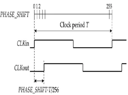
Fig. 2 shows the fine phase shift effects in the fixed mode of operation. A phase-shifted output with a resolution of (1/256)th of the input clock period can be obtained. The variable phase-shifting feature has been used in [3]. However, this operating mode requires several clock cycles to change the duty cycle, degrading the dynamic performance. Besides, an asynchronous circuit is used to divide the clock cycle into four quadrants.
Fig.2.Fixed fine phase shifting effect.
2.2. Generalization of the DCM-based fully synchronous architecture
Let n=m+k be the bits of the duty cycle command dc,
[image:2.595.105.240.329.450.2]319
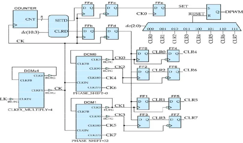
Fig. 3. Implemented high-resolution DPWM with m = 8 and k = 3.
DCMx4 multiplies its input clock frequency by 4. The CLKFX output of DCMx4 is connected to the input clock of the counter, DCM0 and DCM1. The binary counter has 8 bits, and SETD and CLRD signals are generated from the counter output and the eight MSBs of dc as explained earlier. FFa and FFb store these signals. Negative edge-triggered flip-flops FFc and FFd avoid malfunctions due to the phase offset between CK and CK0. DCM0 and DCM1 generate eight phased clocks {ck0…ck7}.PHASE-SHIFT attribute of DCM0 is set to 0. DCM0 generates clocks CK0, CK2, CK4, and CK6. PHASE-SHIFT attribute of DCM1 is set to 32, and its outputs are shifted 32/256 of TCK. DCM1 generates clocks CK1, CK3, CK5, and CK7. In the implementation step of the design flow, DCM0 and DCM1 are manually placed at DCM_X0Y0 and DCM_X1Y0, respectively, in order to be close to each other and reduce routing delays. These two DCMs can drive up to four global clock lines. Then, the circuit must work with the rising and falling edges of only four phased clocks {CK0, CK1, CK2, CK3}, and FF4, FF5, FF6, and FF7 must be negative-edge triggered. This introduces nonlinearity in the on-time step due to duty-cycle variation but this effect cannot be solved due to the routing architecture of this FPGA. For this implementation, the maximum clock frequency is limited to 200 MHz, which is the maximum operating frequency for the CLK90 and
CLK270 DCM outputs according to the FPGA datasheet.
3. DPWM ARCHITECTURE USING IODELAYE1 BLOCK
320
Fig.4. Simplified pinout description of (a) I/O delay elementIODELAYE1and (b) IDELAYCTRL block.
The IODELAYE1 block offers three different operational modes when operating in the unidirectional input delay configuration, depending on the mechanism used to select the number of delay taps.
3.1. Fixed:
The number of delay taps is predefined through the block attributes and it cannot be changed during operation.
3.2. Variable:
The number of delay taps can be dynamically changed after configuration through the control signals CE and INC. When the enable increment/decrement signal (CE) is activated, the number of delay taps increases or decreases depending on whether the INC signal is activated or not. If the reset signal RST is activated, the delay value is reset to a predefined value.
3.3. Loadable variable:
This mode has the same functionality as the variable
mode. In addition to this, it allows loading the delay
value through the 5-bit input CNTVALUEIN. When in this mode, the IODELAYE1 reset signal resets the delay value to a value set by the CNTVALUEIN as shown in fig. below.
Fig.5.IODELAYE1 operation in the loadable variable mode.
3.4. Architecture
Fig.6 shows the proposed implementation for an m+1-bit HRPWM. Basically, the proposed circuit is made up of a synchronous m−4 bit counter, an IODELAYE1 block, two edge triggered flip-flops, an MMCM, and an SR latch whose output is the PWM signal. The main difference with the DCM based architecture is that the multiphase synchronous circuit used to generate the signal RESET is replaced by the IODELAYE1 block, making the implementation easier.
319
Signals SETD and CLRD are generated as previously explained by comparing the counter output CNT with the most m−5 significant bits of the duty command dc(m:5). FFa and FFb are placed in order to avoidthe glitches that may be present in the output of the comparator. For this implementation, the loadable
variable mode for the IODELAYE1 block is used.
The IODELAYE1 block allows, therefore, delaying the input signal through a 5-bit value CNTVALUEIN updated when the NVALUE signal is activated, which has to be synchronized with the clock C.
Considering that the maximum 32-tap delay covers half a period of CK_REF, a clock that doubles the CK_REF frequency is required to clock the counter. These clock signals are generated through the MMCM using as a reference the board base clock CK. The output frequency for the MMCM output i is set through its attributes M, D, and Oi as fCKOi =
M/(D*Oi). In addition to this, the IDELAYCTRL is
instantiated in order to autocalibrate the delay tap as previously explained.
Fig.7. IODELAYE1-based HRPWM operation with dc = “10010011.”
Fig.7 shows the basic operation of the proposed IODELAYE1-based HRPWM architecture with dc = “10010011” The CLRD signal is activated when dc(7:5) = CNT(7:5) = “100” = 4. The resulting pulse is captured in the next clock cycle by FFb, which generates the input signal for the IODELAYE1 block DATAIN. The IODELAYE1 block generates the RESET signal by delaying the CLR signal a number of tap cycles given by dc(4:0) = “10011” = 19. This signal clears the SR latch to generate the desired PWM signal.
4. RESULTS AND DISCUSSIONS
This section presents the main experimental results for the two different PWM architectures. The DPWM signal frequency and duty cycle have been selected for test purposes. Fig.8 shows the experimental results for DCM based HRPWM architecture.
In this stage we give the input to the architecture, we set the clock input value in our implementation side
the clkin act as clock input. If we give the input to the DCM block the output pulse and also the counter values are changed based upon the given input.
Fig.8 Simulation results of DCM based PWM
In this situation we achieve a synchronous in DCM block. In this stage we use the 50 percent duty cycle for the pulse generation which means half the time the pulses will be on and off. The counter value is changed. In first time we set the input value after that the pulses will be generated automatically.By this way we can generate high resolution digital PWM signals.Here ‘n’ is the no:of bits.This allows an efficient HRPWM implementation for low cost systems.
The experimental results for the IODELAYE-1 based HRPWM architecture are shown in fig.9.
Fig.9.Simulation result of IODELAY based PWM
320
generations are based upon the input, here we achieve thesynchronous in IODELAYblock.Through this we can generate the highly efficient and high resolution pwm signals by using the resource present in the high end virtex-6 FPGA series.
This paper details two PWM designs based on the DCM the IODELAYE1 blocks available in modern FPGAs.
TABLE I
PROPOSED HRPWM ARCHITECTURES COMPARISON
Architectur e
Coarse counter frequency
Resoluti on
Paths to equilib rate
Fully synchr onous
Glitch free
DCM 200MHz 625ps 8 Yes Yes
IODELAY 200MHz 78ps 1 Yes Yes
In Table I, we summarize the characteristics of the proposed HRPWM architectures. This architecture achieves higher resolution, while keeping a fully synchronous design. Besides, these are glitch-free designs, which improve the circuit reliability, and the number of paths to equilibrate in order to achieve a monotonic behavior is minimized.
5. CONCLUSION
The proposed DCM-based and IODELAYE1-based synchronous architectures have been designed on a Xilinx Spartan-3E and Virtex-6 FPGA, respectively. The experimental results show a resolution of 625ps for the DCM-based architecture, 78ps for the IODELAYE1-based architecture, and 19.5ps for the HRPWM architecture. The selection of the target device depends on the system cost and resolution requirements. The PWM developed can be used in many diverse and complex applications like robotics, motor and motion control.
Acknowledgment
First the Author thanks to god and also wish to thanks the management of Loyola institute of technology and science for providing the excellent computing facility and encouragement.
References
[1] Angel Vpeterchev, “Digital pulse width modulation in power electronic circuits,” July2002.
[2] S. Mekhilef and A. Masaoud, "Xilinx FPGA based multilevel PWM single phase inverter," 2006 Engineering e-Transaction, vol.l, no.2, pp 40-45, Dec. 2006.
[3] A. de Castro and E. Todorovich, “DPWM based on FPGA clock phase shifting with time resolution under 100 ps,” in
Proc. IEEE Power Electron. Spec. Conf., 2008, pp. 3054–3059.
[4] A. M. Omar, N. A. Rahim and S. Mekhilef, 'Three-phase synchronous PWM for flyback converter with power-factor correction using FPGA ASIC design," IEEE Trans. Ind. Electron., vol. 51, no. I, pp. 96-106,Feb. 2004.
[5] A. Myaing and V. Dinavahi, "FPGA-based real-time emulation of power electronic system with detailed representation of device characteristics", IEEE Trans. Ind. Electron., vol. 58, no. I, pp. 358-368, Jan. 2011.
[6] A. Syed, E. Ahmed, D.Maksimovic, and E. Alarcon, “Digital pulse width modulator architectures,” in Proc. IEEE Power
Electron. Spec. Conf., Jun. 2004, vol. 6, pp. 4689–4695.
[7] A. de Castro and E. Todorovich, “High resolution FPGA DPWM based on variable clock phase shifting,” IEEE Trans.
Power Electron., vol. 25, no. 5, pp. 1115–1119, May 2010.
[8] Denis Navarro, Oscar Lucia, Member, IEEE, Jose Ignacio Artigas, Isidro Urriza, and Oscar Jimenez, Student Member
IEEE“Synchronous FPGA-BasedHigh-Resolution
Implementations of Digital Pulse-Width Modulators‟ IEEE
Transactions On Power Electronics, Vol. 27, No. 5, May 2012. [9] TMS3 20x28xx, “High-resolution pulse width modulator (HRPWM),”Reference Guide, Texas Instruments SPRU924C, Dallas, TX, 2007.
[10] Spartan-3 Generation FPGA User Guide, UG331 (v
1.5), Xilinx, San Jose, CA, 2009, ch. 3.
Anupama.s received the B.E degree in
Electronics and Communication