e·
e
e
e
e
e
e
e
e
e-e
e·
e
e
e
e
e
e
e
e
e
e·
Customer
Engine~'rin'g
<&l
Manual of Instruction
Series Data Processing Systems
Component Circuits
Book
A.
General Theory
Book B. 701-704-709 Components
Book C. 702-705 Components
Book
D.
Auxiliary Equipment
Book
E.
Appendix
7
/.
c,
)
I.
"-'I
I·
.j
,1 "
h \ C. f· \
\l
L
I I ' " / , ..
~ J",
I .. ,
" ,,,,I, ,
(
J c·
I·. \1\ l
,. i ,\ I
.'
I ; ~ ,.A ,',I" (" \ 'i!' ~t , ..
ii, I J i . \ , ; - , ,
/
\' \rv ..
. .j
( , '
" • \ \··.,1 J' . '. I'.
\ 1 ,
"
.\
~ \
" I
)
,
\ .'" .' l. i
I
\ .
I ..
Issued to: /1 U
J.'
, V ~, . \Department or " Telephone • o.
Branch .ffice'---">.J),-,-~...!.I...!.(-,-' :...' _ _ _ _ _ Number ' . ' , I -'
Address,_\:",'_·_-=-\'.:...\~J-_'.2·),-""--,,I'"'-/ _ _ _ _ City ' 4 ( " , tlltState
Cl
';,~ ~If this manual is mislaid, please notify the above address.
© 1955, 1956, 1957, 1959 by
International Business Machines Corporation 590 Madison Avenue, New York 22, N. Y. Printed in U. S. A.
This manual is written at a level that assumes the reader has a background of basic electronics. The text material is not written from a standpoint of design but rather from a standpoint of the circuit understanding that is necessary for servicing. Where design information is deemed necessary, it is included. For those who feel a need for review, the Appendix (Book E) contains formulas and procedures necessary for simple computations of voltage levels and currents flowing in the circuits. Book E also contains some design procedures for those who want more material on this subject.
Data-processing machines, such as the 700 series machines, contain many thousands of individual electronic components (resistors, capacitors, inductors, electron tubes, crystal diodes, and so on). Together, they form the "nerve system" of the calculator. Because of the complexity of showing the miles of circuits that make up these machines, the logic block method of circuit layout is used. Logic blocks simplify circuit tracing and trouble shooting. Each logic block represents an individual circuit. Each circuit has a specific function in the area where it is used. With the logic block method, cir-cuits are easily identified and the location of each component is easily found. The fol-lowing pages contain the logic blocks of component circuits, the circuit schematics, their purpose, how the circuits function, the inputs, and the resultant nominal outputs of these circuits. Given voltage levels and wave forms are suggested values only, as loading conditions affect individual circuits in the machine.
This manual is divided into five main books.
Book A contains information that is pertinent to all component circuits and should be studied before investigating any individual circuit. The location procedure is de-scribed early in the manual so that it may be reviewed with each circuit until it is fully understood.
Book A also describes circuits that are popularly called basic or standard circuits. Because these circuits are most commonly used, a thorough study of them helps the customer engineer in understanding the remaining circuits. For this reason, they are explained in greater detail than circuits that are merely modifications of the standard circuits.
Book B contains information about the pluggable unit panels, the systems block dia-grams and the MF neon locations peculiar to the 701, 704, and 709 machines. It also has a complete listing of component circuits assigned to the 701, 704, and 709 systems except power supply and transistor components. Every circuit listed in this book is cross-referred to the "4" pages of machine systems, e. g., inverter I (section 2.01. 01, Book B) is the same as 4.01. 01 and key trigger TK (section 2. 02. 05, Book B) is the same as 4.02.05. Wherever advisable, the reader is referred to Book A for a more detailed description of the circuit.
Also, this book contains a complete listing of component circuits except power supply components. The basic circuits are duplicated here, with the reader referred to Book A for a complete description. This duplication is made so that circuits listed in this section can have cross reference to the "C" pages of machine systems. ("C" pages contain circuit schematic and standard pluggable unit wiring procedure.) An
example is the inverter I (section 2.01. 01, Book C) which is the same as C. 01. 01 and key trigger TK (section 2.02.04, Book C) which is the same as C. 02. 04. Circuits that appear in isolated areas such as memory or drum alone are briefly discussed here but full discussion of their usage is found in the respective machine manuals.
Book D contains information and the component circuits for the 700 series auxiliary equipment. The machines described in this book are the 720 Printer, the 760 Control and Record Storage Unit, the 774 Tape Data Selector, and'the 777 Tape Record Coor-dinator.
NOTICE
The text and illustrations included in the following pages have been prepared for teaching purposes and as an aid for learning the component circuits of the 700 series machines. All material was prepared from information relative to production at a given level. Engineering changes may alter exact timings, logic blocks or component values; therefore, the customer engineer is advised not to use this information alone as a reference manual or servicing aid.
ABBREVIA TIONS
The following abbreviations are used throughout this manual. Component circuits block designations (such as I for inverter) are not included in this list.
A all (cycles) inst instruction
a ampere
I/o
input/outputAC alternating current K kilo (10 3) (usually refers to ohms)
adr address Kc kilocycles
amp amplifier L inductor
bksp backspace It left
C capacitor meg megohms (106 )
C cycle m milli (10-3)
CB circuit breaker MF main frame
CF core frame MQ multiplier quotient
CP card punch
.n.
ohmCPU central processing unit op operation
CT cycle time Pr printer
CS core storage Q quotient
ctr counter R resistance
DC direct current rewd rewind
DF drum frame RI read-in
e voltage rt right
E execute (time) Rd read
EC edge connector S (sec) seconds
EOF end of file sw switch
EOR end of record stg storage
f farad tgr trigger
h henry u micro (10-6)
I current uu micro-micro (10- 12)
I instruction v,V volt
e
e
e
e
e
e
e
e
e
e
e
e
e
e
e
e
e
e
e
e
e
e
e
e
e
e
e
e
e
e
e
e
e
e
e
e
e
e
e
e
e
e
Component Circuits
I
I
I
I
I
I
I
I
I
I
I
I
I
I
I
I
I
I
I
I
--
e
CONTENTSSection Title Symbol Page
-
1. 00. 00 GENERAL INFORMATION. A 51. 01. 00 Definition of Terms . A 5
e
1. 02. 00 Pluggable Unit. A 51. 03.00 Pluggable Unit Location A 7
1. 04.00 Pulse Sketches and Wave Forms. A 7
e
1. 05. 00 Input/Output Levels A 91. 06. 00 Crystal Diodes. A 9
1. 07. 00 Electron Tubes A10
e
1. 08. 00 Circuit Delays. All2.00.00 STANDARD CIRCUITS A13
e
2.01. 00 +AND (-OR) Circuit..
A • A132.01. 01 Circuit Description A13
2.01. 02 Rise/Fall Time A15
e
2.02.00 +OR (-AND) Circuit . 0 A152.02.01 Circuit Description A15
2.02.02 Rise/Fall Time
.
A17e
2.03.00 +AND Driving +OR Circuit. • A172.03.01 Circuit Description A17
e
2.03.02 Rise/Fall Time A192.04.00 Diode Cascading . • A19
2.05.00 Inverter.
.
I, lK A23e
2.05.01 Circuit Description A232.05.02 Compensated Output. • A23
2.06.00 Trigger. T A27
e
2.06.01 On and Off Convention for Trigger A272.06.02 General Trigger Circuit Operation • A27
2.06.03 Specific Components in a Trigger A27
e
2.06.04 Electronic Reset • A292.06.05 Manual Reset . A29
2.06.06 Inputs to a Trigger • A29
e
2.06.07 Input Requirements for the Trigger . A342.06.08 Outputs from the Trigger . • A34
2.06.09 Voltage Levels in the Trigger. • A34
e
2.06.10 Block Representation of theHigh-Speed Trigger . • A34
2.06.11 Special Features . A35
e
2.06.12 Application of Triggers . A352.07.00 Diode Gate • DG· A39
2.07.01 Circuit Description A39
e
2.07.02 Variations . • A392.08.00 Diode Gate.
.
GJ . A412.08.01 Circuit Description A41
e
2.09.00 Cathode Follower. K A432.09.01 Circuit Description A43
2.09.02 Positively Returned Resistive Load. A45
e
2.09.03 Negatively Returned Resistive Load A452.09.04 Capacitive Load
.
A45e
Section 2.09.05 2.09.06 2.09.07 2.09.08 2.10.00 2.10.01 2.10.02 2.10.03 2.11. 00 2.11.01 2.11. 02 2.11. 03 2.11.04 2.11.05 2.11. 06 2.11.07 2.11. 08 2.12.00 2.12.01 2.12.02 2.13.00 2.13.01 2.14.00 2.14.01 2.15.00 2.15.01 2.15.02 Title
CONTENTS (continued)
Parallel Cathode Follower Cathode Follower OR Circuit . Cathode Follower Inputs Summary
Grounded-Grid Amplifier Circuit Description Variation
Variation Single Shot .
Circuit Description Recovery Time Timing Accuracy. Inputs
Outputs . Miscellaneous. Variation Outputs .
Pulse Forming Inverter. Circuit Description I Timing.. OscRrator (Clock).
Circuit Description • Thyratron Circuits .
Printer/Punch Magnet Thyratron Peaker .
Principles of Peaker Circuit Operation Wave-Form Generator Peaker
e
e
e
Symbol Page
A45
e
A46
A46
e
A46
GAF A49
A49
e
1/2 GAF . • A49
GA FO A50
SSE A53
e
A53 A55
A55
e
A55 A55
A56
e
SSF A56
SSF • A56
IpF A59
e
A59 A59
e
OSC A61
A61 A62
e
TH A63
PKR A65
A65
e
PKRZ· A66
1. 00.00 GENERAL INFORMATION
1. 01. 00 DEFINITION OF TERMS
Certain terms in the circuit descriptions must be clarified or defined, e. g. , "standard cathode follower" or "standard inverter." All circuits are standard but the basic ones (such as AND, OR, I, K, T, and S8) are the most commonly used. Others may be merely modifications of these basic circuits or entirely different circuits; they are popularly called "special circuits, " used in a very few applications.
The term "tube" may refer to one or both sections of a dual tube, but the term is not used unless the reference is clear in the text. The terms "left tube" and "right tube" refer to the placement of the components on the schematic. They are not to be confused with the terms "front" and "back" that are used to denote the physical placement of the tube socket on the pluggable unit.
The voltage levels of the pulses and input/output lines fall into two general class-ifications: signal level and plate level (section 1. 05. 00). The terms "rise" and "faIP' refer to the transition of a pulse. Rise or fall time is usually the time
re-quired for a pulse transition to reach 80 percent of its final value (from ten percent to 90 percent). Rise and fall time of a pulse is expressed in volts per microsecond (millionth of a second). Pulse width is measured at a point halfway between voltage levels.
Electron flow ( - to + ) is assumed in all circuit descriptions. Increasing the ab-solute potential gradient across a capacitor is called charging the capacitor. When this gradient decreases, the capacitor is discharging. During some types of
transitions, the polarity of the voltage across the capacitor reverses; therefore, the terms "charge" and "discharge" as defined above may be confusing. In these cases assume that one terminal of the capacitor is connected to a steady voltage which is always more negative than the opposite terminal. H this assumption is made, the above definitions of charge and discharge still apply. For example, if the voltage at one terminal of a capacitor changes from -30 volts to +10 volts and the opposite terminal is grounded, assume then that the capacitor has been charged.
It discharges when the voltage returns to -30 volts. 1. 02. 00 PLUGGABLE UNIT
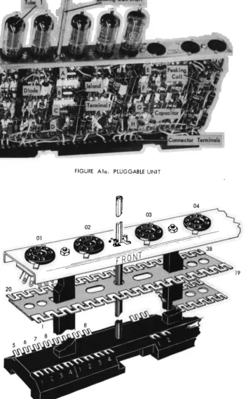
The pluggable unit acts as the carrier for most of the component circuitry (tubes, resistors, capacitors, and so on) in the 700 series systems (Figures Ala and Alb). The unit has eight tube sockets, although it need not have the full complement of eight tubes. Filament terminals of all tube sockets are wired.
FIGURE Ala. PLUGGABLE UNIT
FIGURE Alb. PLUGGABLE UNIT
e
e
e
e
e
e
e
e
e
e
e
e
e
e
e
e
e
e
e
e
[image:12.614.130.482.109.678.2]Mounted within the pluggable unit are eight terminal strips each consisting of 38 solder terminals or lugs. The terminals are numbered 1-19 on the fnmt of the unit and 20-38 on the back. The terminals are initially shorted together and cut open to make the terminals individual. This procedure eliminates the need for jumpers. The terminal strips are called islands and are located by their corresponding positions in the unit (A through H). The circuit components are mounted between these islands.
Directly beneath each tube position, at the base of the unit, is a group of con-nector terminals labeled 1 through 8. These terminals are internally connected to the male knife connectors beneath the base. The unit connects to a female receptacle that has solder lugs extending out on the wiring side of the panel (panel pins). There are eight panel pins for each tube position. The panel pins are used for the entry of service wiring (voltage supplies) and signal wiring to the unit.
The locking-cam shaft extends through the unit and is used to seat the unit into its female connector. The unit is aligned to the connector; rotating the shaft with a pluggable unit wrench cams the unit downward to lock it in place. The contacts on the female connector are aligned vertically in such a way that the negative voltages are applied before the positive voltages when the unit is installed. The reverse is true when the unit is removed. However, it is wise to drop DC voltages before removing or installing pluggable units.
Each machine systems index section has a pluggable unit location chart for each panel on the machine. This chart includes unit part numbers. Standardization of units is retained wherever possible. Thus, the same units may have components used on one machine and unused on another.
1. 03.00 PLUGGABLE UNIT LOCATION
All panels that contain pluggable units use the coordinate reference system for locating specific points on the panel. The vertical axis is labeled with upper case letters A-Z, omitting I and O. The horizontal axis is labeled with numbers 01-40, the number of columns depending upon the specific unit. Thus, the intersection of a horizontal and a vertical notation locates a specific section of the panel. Location is given to any pluggable unit in the panel by giving the column and alphabetic lo-cation of the first tube of the unit. With eight tube positions per unit, the first tube locations can be only A, J, or S. Because the islands are lettered and the island terminals are numbered, any component on a unit can be located. Panel pins re-ceive their location from the tube socket that is in line with the pin group.
1. 04. 00 PULSE SKETCHES AND WAVE FORMS
Sketches and wave form drawings are included to aid circuit explanation. For drawing convenience, pulse sketches are shown in many cases as a square wave, although the perfect square wave (zero rise and fall time) does not exist. Actual rise and fall time is usually several tenths of a microsecond. Distortion effects of a circuit on an incoming pulse are occasionally overemphasized to show graph-ically what is causing the distortion. Also, poor input pulses are used to show pulse-shaping and level-setting characteristics of a circuit.
The same circuit can operate differently throughout the machine because of var-iables such as stray capacitance, output loading, and variations in component toler-ances.
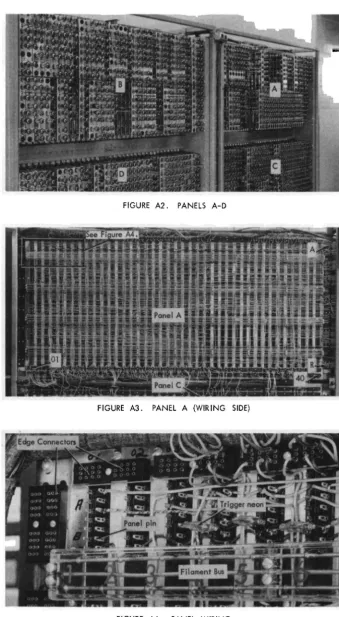
FIGURE A2. PANELS A-D
FIGURE A3. PANEL A (WIRING SIDE)
FIGURE A4. PANEL WIRING
e
e
e
e
e
e
e
e
e
e
e
e
e
e
e
e
e
e
e
e
e
[image:14.618.127.467.84.702.2]1. 05. 00 INPUT/OUTPUT LEVE LS
The voltage levels of pulses and information lines fall into two classifications: signal level and plate level. Signal levels are developed at divider outputs while plate levels are developed at full plate, tapped plate, or tapped divider outputs.
Signal level limits are usually +10 to -30 volts, with certain circuits requiring variations. In high-speed computer circuits, the effect of line capacitance to ground is detrimental. Therefore, the voltage swing above and below ground was chosen as a minimum satisfactory level. Circuits are controlled by the input rise from -30 to +10 volts, the fall from +10 to -30 volts (± shift inputs), or the steady up or down level. The rate of change from one voltage level to another must usually be fast (60 volts/microsecond). Some circuits have adverse effects on the voltage shift; they damp or cut down the amplitude, slow the shift time, or cause general distortion. Other circuits overcome these faults with their pulse-shaping and level-setting characteristics.
Because plate levels are about 100 volts, they are noted as plate levels in the system pages. This notation is an aid to proper sensitivity settings on the oscil-loscope or voltmeter. Plate level outputs are used for economical component usage. They perform the same duty as signal levels.
1. 06. 00 CRYSTAL DIODES
Crystal diodes rather than vacuum tube diodes are used in the machine wherever possible. The small crystal diodes have an obvious advantage in size over their counterpart in vacuum tubes; they have the added advantage of not needing a filament or heater, thus reducing power requirements and wattage loss in heat. Because the number of diodes employed is large, these are distinct advantages. Many watts are saved by their use and thousands of unwanted BTU's of heat are avoided. The symbol used for the crystal diode is shown below with plate and cathode labeled.
cathode
~~-p-l-a-t-e---Crystal diodes are divided into various classes depending on their back and for-ward resistance and upon their ability to pass current. Back resistance is the DC resistance exhibited by a diode when the cathode is more positive than the plate. With the cathode more positive than the plate, the diode is theoretically cut off. For-ward resistance is the opposite of this, or the resistance exhibited by a diode when the plate is more positive than the cathode. Diode specifications and identification markings, as well as theory and construction, are listed in the Appendix (sections
1. 01. 05 and 1. 02. 04, Book E).
1. 07.00 ELECTRON TUBES
The three most commonly used tubes in the 700 series are the 6211, 5965 and 5687. The tubes are listed in the order of their usage in the system. The 6211 is most used because it has the lowest filament current requirements and the 5687 is used only where maximum power is needed. The three tubes are 12. 6v dual triodes with center tapped filaments so that either a 6.3 vor 12. 6v filament supply can be used.
The filament transformers are center tapped to either ground or a minus voltage. The AC value is thereby superimposed on different DC levels. Keeping the filament supply at a certain DC level minimizes the potential difference between cathode and heater (a manufacturer's tube specification). In sensitive amplifier circuits, this procedure also is used to prevent the cathode from being positive with respect to the filament and causing current flow from filament to cathode. Detrimental noise would be introduced into the amplifier circuit. See Figure E10 for the filament wiring lay-out. Note that the panel pins are different for each voltage level; thus, a 6v pluggable unit is inoperative in a 12v pluggable unit socket, preventing damage to the filaments. The four tube groups are fed by the filament bus in such a manner as to have the filament current travel the same bus bar distance regardless of the tap-off position. Therefore, the filament supply voltage is uniform along the complete length of the bus bar.
In most tube circuits, the status of the tube is either cut off or in full conduction, and full conduction is usually only two-thirds of recommended maximum current. In
other circuits, where maximum current is exceeded, the duty cycle is very short. The duty cycle is based on a time of 30 seconds. Thus, a ten percent duty cycle indicates that the tube is operating or conducting about three seconds out of every 30 seconds. The individual durations of conduction are usually in the order of fractional parts of a microsecond and the average of these durations meets the above specifications. Because of the two basic conditions (conducting or cut-off), the cut-off bias is frequently used in circuit description.
These voltages are: 6211 5965 5687
-8.5 volts -6.5 volts -13 volts
Most tubes contain a 150-ohm parasitic suppression resistor in the grid circuit. Omission on the circuit schematic does not imply that this resistor is missing. In circuit design, modifications are made to insure proper operation with tubes falling in the classification 25 percent weak to 20 percent hot. Other tube specifications are listed in the Appendix.
1. 08. 00 CmCUIT DELAYS
A characteristic of many tube circuits is the delays that are produced. Delay is defined as the time elapsing between the beginning of a voltage shift at a grid and the beginning of a resultant shift at the plate. Because a positive input pulse starts from a level of about -15 to -30 volts and must rise to the cut-off point for the tube before any conduction occurs, the time required to rise to this point appears as delay in the output. Conversely, any time required for an input pulse to fall from the nominal +lOv level (where grid current flows) to ground (where grid current ceases) also appears as a delay in the output. Therefore, the slower the voltage transition at the grid, the more delay produced at the plate. This delay can be approximated as roughly one half of the rise or fall time of the input pulse. Delay of a circuit should not be confused with rise and fall time characteristics.
IN 1
IN 2
(a)
+140
*Terminal 14 on Island C
~T
* Point B is terminal 14 on island C.
+140
-30 -30
-30
(b)
+140
+10
,
-30..
-
-=..L:--30 '"1'
....L..
-(c)
-+140
+10
~
-
=.!..=-+10 ....L. ~
(d)
+140
-30
++...J....++
+10 ....L l '
(e)
IN 1
~
IN 2
OUT
(f)
~ MF3 J28
~
ANEr
~
xxx Is RL In kdohms returned to
+ 220 volts for a + AND circuit in the 704 system
+10
-30
+10
L
-30+10
(
-30..
time
R1
I
As
:il
R2
[image:18.617.87.559.58.733.2]2.00.00 STANDARD CIRCUITS
The circuits in this section are popularly called standard or basic circuits be-cause of their frequent usage in the system. The circuits are kept in one section as an aid to a thorough understanding of their operation and early application to machine logic.
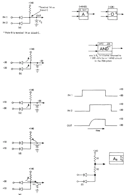
2.01. 00 + AND (-OR) CIRCUIT
The +AND circuit in Figure A5 is the first of four basic diode circuits used. Diode circuits form the basis for switching, decoding, adder, sampling and control circuits. They are economical because they use few components and require no vacuum tubes.
The circuit configuration for the +AND and the -OR are identical. The polarity designations are adopted in order to work with negative logic, that is, the recogni-tion of the absence as well as presence of informarecogni-tion. Logical operarecogni-tion of these two circuits is as follows:
+AND circuit requires all inputs to be plus for a plus output.
-OR circuit gives a minus output if any input is minus.
Each description holds true for either circuit because the circuits are identical. However, the logical usage is different. The +AND insures that both inputs are up before the output comes up, while the -OR gives a minus output as long as any input is down.
Figure A5f is the logic block and circuit configuration for the tapped-output AND circuit AB . Thus, an output higher than +l0 volts is obtainable. The infor-mation in the upper portion of the logic block locates the junction point of the two resistors. This pOint is the tap. It represents the output of the A
B.
2. 01. 01 Circuit Description
Figure A5a shows the junction point of the diodes and the resistor (R). This point is always used to locate diode circuits within pluggable units. Resistor (R) limits current and controls the rise time of the output. C
s
represents input cap-acity of the circuit being driven and stray wiring capcap-acity.If both inputs are at -30 volts, the polarity is correct for both diodes to conduct (Figure A5b). The resultant current flow through R causes a voltage drop across it
to maintain a level of about -30 volts. Because of the diode's forward resistance of 100 ohms, the voltage at the junction will be -29. 04 volts. For practical purposes, the output is -30 volts and C
s
is discharged.If input 1 changes instantaneously to +10 volts, diode 1 is cut off because the cathode is more positive than the plate (Figure A5c). Diode 2, with -30 volts on its cathode, maintains conduction and the output remains unchanged. There is a small amount of current flowing through diode 2 to the +lOv source, but its effect is negligible.
IN 1
IN 2
-30
-30
+10
-30
<r-{>I-(e)
-30
-30
I
-130
Terminal 34 on Island G
,
~
I
-130
---130-D
:I~FR~ ~
~
I
DEl A10f _ _ •OR
yxY .~
. R in kilohms, returned to
YYY IS L +OR circuit in the 704
-250v for a system.
IN 1
I
IN 2
+10
-30
+10
-30
+10
~-30
I
OUTFIGURE A6. +OR (-AND) CIRCUIT
-e
e
e
e
e
e
e
e
e
e
e
When input 2 changes to +10 volts, diode 2 is cut off because Cs momentarily is holding the output at -30 volts (Figure A5d). Cs has to charge through R to +140 volts and this delays the rise of the output level. The voltage level at the junction starts heading for +140 volts but, as soon as +10 volts is reached, the diodes go back into conduction. The output is now +10 volts and Cs is charged to +10 volts.
When input 1 falls to -30 volts, diode 1 conducts harder, discharges Cs ' and diode 2 is cut off (Figure A5e). The output follows the input down to -30 volts and Cs is discharged. When input 2 falls to -30 volts, diode 2 goes back into conduction to help maintain the -30 volts output.
The action of an AND circuit may be summarized as follows: The output voltage of an AND circuit approximately equals the most negative input voltage. This state-ment is true regardless of the number of inputs.
2. 01. 02 Rise/Fall Time
The fall time of an AND circuit usually follows the input. However, the rise time depends upon the time constant of an RC circuit and is delayed. In circuit design where the value of Cs and the desired rise time is known, this formula de-termines the value of the limiting resistor. By transient analysis the formula for calculating rise time is:
Rise Time
-30 volts to +10 volts
2.02.00 +OR (-AND) CIRCUIT
t =
~: g~g Hg~:+g~~
R in megohms C in uuf (Cs) tin usec
The circuit configurations for +OR and the -AND circuits are identical. Logical operation of these two circuits is:
+OR circuit gives a plus output, if an input is plus.
-AND circuit requires that all inputs be minus for a minus output.
Therefore, the +OR circuit differs from the +AND circuit in that it needs only one input up to bring the output up.
2.02.01 Circuit Description
If both inputs are at -30 volts, the polarity is correct for both diodes to conduct (Figure A6b). The voltage drop across the limiting resistor sets the output level at about -30 volts and Cs is discharged.
If either input rises to +10 volts, that leg conducts harder and provides a charge path for Cs (Figure A6c). The other diode cuts off and the output follows the input
+140
IN 1
IN 2 n---K
(a)
+10
-30
:
B
.:>t---1!"'-/_r--....-
OUTR (OR)
-130
_ I
"'-'c
- L S
L -_ _ _ _ INI
+10 _ _ _ _ _ _ _ _ _ _ _ _ _ _ _ _ _ _ _ _ _ _ _ _ _ _ IN2
+10
(
-30 A
+10
-30
(
~
BFIGURE A7. + AND DRIVING + OR
e
e
e
e
e
e
e
e
e
e
e
e
e
e
e
e
e
e
e
e
e
in rising to +10 volts. It is normal for only one input to an OR circuit to come up at a time.
When the input that was up at +10 volts drops to -30 volts, Cs momentarily is still charged to +10 volts, and the input diode is cut off (Figure A6d). This means that the fall time of the output is delayed because Cs maintains a plus voltage until it is discharged through R. The RCS time constant controls the fall time of the OR output. The input diodes again conduct when the level at the junction reaches a pOint slightly more plus than -30 volts.
The action of an OR circuit is summarized as follows: The output voltage of an OR circuit apprOXimately equals the most positive input voltage.
2.02.02 Rise/Fall Time
The rise time of an OR circuit usually follows the input. However, the fall time is now the affected part of the output and depends upon an RC delay. Fall time of an OR circuit is computed by the following formula:
Fall Time t = O. 17RC (701-704) 0.34RC (702-705) +10 volts to -30 volts R in megohms
C in uuf tin usec
2.03.00 +AND CmCUIT DRIVING +OR CIRCUIT
Throughout the system, AND/OR circuits are tied together to form a network that decodes, adds or multiplies. A common situation is: AND circuits drive OR circuits. The circuit configuration is shown in Figure A 7a.
2.03.01 Circuit Description
Assume the following initial status:
Inputs 1 and 3 at -30 volts Input 2 at +10 volts
The voltage at point A is about -30 volts because D1 conducts through R (AND). Parallel current also flows up through R (OR), through D4, and through R (AND). The parallel current does not affect the voltage level at point A because Dl con-trols the level. Point A, being at -30 volts, sets the output level at -30 volts; Cs is discharged.
Input 1 is changed to +10 volts, D1 and D2 are momentarily cut off because Cs holds the output at -30 volts. D4 conducts; as point B starts to rise, D3 is cut off. Neglecting the effect of diode back resistances, the output rises exponentially from -30 volts toward a voltage determined by the DC voltage division between R (AND) and R (OR). This is the DC voltage that would be present at the output if diodes D1, D2, and D3 were disconnected from the circuit. (Design practice sets this level at about +20 volts). Cs charges toward this voltage and is clamped at +10 volts by the input. Note that if R (AND) was too large, the diodes would remain cut off and the output would never reach +10 volts.
+140
R (AND)
- 3
°o--K
r---t---~+ 1 Ov----,,, r - - - - 1
+10
+l0o--K r - - - - 1
+ 10''''--_1r ~----1
+lOo--K r - - - - '
(a)
+140
(c)
Cascaded
R
R8 = 400K
each leg
-30
+10
3AC'~
+140
R
-30
+10
SOK
Equivalent Circuit
+140
R
170K
Equivalent Circuit
(Cascaded)
(d)
(b)
FIGURE AS. CASCADED +AND CIRCUIT
e
e
e
e
e
e
e
e
e
e
e
e
e
e
e
e
e
e
e
e
When either input 1 or 2 falls to -30 volts, the respective diode conducting causes point A to fall immediately to -30 volts. D4 is cut off because point B can-not change until C
s
discharges. Normal OR circuit fall-time delay takes place and the output falls exponentially to -30 volts.2.03.02 Rise/Fall Time
It has been shown that the output of a +AND driving a +OR combines the rise/fall time delays of both circuits. However, the rise time formula listed in section 2.01. 00 does not apply here. The formula is based on the percentage of the total circuit volt-age the output has to swing. For example, the rise time for a +AND circuit is given as t = O. 27RC. The O. 27RC comes from universal time constant curve (Figure S9). The voltage limits in the +AND are +140 volts and -30 volts for a total of 170 volts. The output swing is 40 volts. Thus the percent of output switch is 40/170 or 23.5 percent. This percent of transition intersects the curve at O. 27RC (time
con-stant) and hence, the rise time formula. In the case of the AND/OR, the total equivalent voltage that the output sees has to be computed by Thevenin's Theorem (section 1. 01. 01, Book E). By computing the fraction 40/E eq + 30 volts) and by using tLe curve in Figure E2, the number of time constants (t/T) corresponding to this fraction can be found. With this value use the following formula to compute the rise time of the AND/OR combination:
Rise Time
-30 volts to +10 volts
t=Req C tiT R in megohms C in uuf Tin usec
The fall time of a +OR circuit driving a +AND circuit can be computed in a simi-1ar manner.
2.04.00 DIODE CASCADING
The back resistances of the diodes in AND/OR circuits act as a load on the driv-ing circuits. When this effective back resistance is too low, the drivdriv-ing source (another diode circuit or cathode follower) cannot supply enough current to main-tain proper down levels or mainmain-tain required rise/fall times. Diode AND/OR circuits with 5,6, and 7 inputs are used and these circuits present the problem of lowered effective back resistance.
A six input AND circuit is shown in Figure AS before and after cascading. Back resistance of an AND circuit is especially important when only one input is at -30 volts and is maintaining the output down level. This condition is shown in Figure ASa. Assume that each diode has a back resistance value of 400K. Each input that is at +10 volts can be represented as a resistor of 400K because each of these diodes is cut off. Five resistors of 400K in parallel give an equivalent resistance value of SOK as shown in Figure ASb. Therefore, the SOK acts as additional load to the -30v driving source.
When a diode is placed in series with each pair of input diodes (A8c), effective back resistance is increased to 170K (ASd). The driving source now sees almost twice as much resistance offered by the inputs. Cascading cuts down the current requirements for this circuit. If the -30v input is a high impedance source (such
as
an OR circuit), excess current drawn by cut-off diodes can raise the down level. Low impedance sources are also limited as to the amount of current that can be supplied to a positively returned load.Multiple input OR circuits present the same problem when all inputs are down at -30 volts except one. The one leg rising to +10 volts must handle the charging current from Cs and the cut-off diodes. The lowered back resistance of the cut-off diodes affects rise time and cascading increases the needed back resistance.
The original design of AND/OR circuit networks determines whether cascading saves tubes or simply represents a waste of diodes.
Cascaded AND/OR circuits are designated AC and 0C' respectively, in logic blocks. An example of AND/OR usage is shown in the Appendix and in the illus-tration "12 to 6 Translator. "
e
e
e
NOTES
e
e
e
e
e
e
e
e
e
e
e
e
e
e
e
e
e
e
A21In
Circuit
Tapped Out _ _ _ ....J
(a)
+139
(b)
+99 ~--1
+140
250 uh
6211
Z
--130
. - -... +10
-130
~
0.23maI
+61 FullConduction
12.3 ma
. (c)
_ _ ~-30
-130
8.2 uuf or
15 uuf
Divider Out
Logic Block
+8
IN
-20
+10----1
OUT
(d)
Compensated Output
~C~
up,.,w~.-.: ~
Middle Wave - lcR~
Lower Wave - Sum of upper
I I
and middle
~
L
wave
(e)
Effect of Peaking Coil
,-
.
.
', ~
I
,.
/
I
(f)
2.05.00 INVERTER (I) (IK)
The standard inverter in the 700 series is the high-speed inverter (Figure A9). The inverter circuit produces a negative shift at its plate when a positive shift is applied to the grid, and a positive shift at its plate when a negative shift is applied to the grid. This property makes it useful in inverting logical conditions, such as changing binary zeros to binary ones. The inverter is also a level setter and pulse shaper because of its amplification properties.
The large resistance in the plate circuit gives a large voltage swing, but does not slow down the signal transition appreciably. The coil in the plate circuit speeds the rise of the plate voltage. When the tube is cut off, the coil produces a voltage which for a short time makes the plate more positive than it would be without the coil. The coil causes a slight overshoot in this rise of the plate voltage but has practically no effect upon the fall time of the circuit. The effect of this coil on the voltage at the plate is shown in Figure A9f. The lower dotted line represents the voltage without the coil; the upper overshoot represents the voltage produced by the coil. The resultant shape of the voltage shows the tendency to square the rise; this results in a fast-rising voltage at the plate. The 10K resistor and its by-pass cap-acitor are used for grid current limiting when a low impedance driving circuit is used. The inverter has a nominal rise time of O. 2 usec (microsecond) and a fall time of 0.25 usec. An IK is the same circuit but uses one half of a 5965 tube.
2. 05. 01 Circuit Description
The minimum input requirements are +5 volts and -13 volts. Assume that the in-put voltage is -20 volts. The tube is well beyond cut-off because cut-off bias is -8.5 volts for a 6211 .. The divider output is at +10 volts because 0.33 rna are flowing through the divider circuit (Figure A9b). The DC resistance of the coil (25 ohms) is di sregarded.
When the input rises to +5 volts or higher, the tube is in full conduction (Figure A9c). With a load of 6. 3K, tube current is found to be about 12.3 rna. Grid current keeps the grid slightly above ground. The current flowing through the plate load causes the voltage at the plate to drop to +62 volts. However, the divider circuit is tied to the plate and the +62v level. Divider current drops to O. 23 rna and this cur-rent adds to the tube curcur-rent through the plate load. The voltage at the plate is low-ered to +62 volts and the divider output is -30 volts. Although this method of calcu-lating plate current is an approximation, its simplicity overrules the small error involved.
The level-setting characteristic of the inverter circuit is shown in Figure A9d. Because the circuit is fully operated by only a portion of the input pulse, the ampli-fication of the tube resets the levels of the pulse. Pulse shaping is aided by both the amplification and the action of the peaking coil.
2.05.02 Compensated Output
The circuit produces a fast rise and fall at the plate. This voltage shift must be fed to the next circuit where stray capacitance acts upon the shift. Figure Age shows that if Cs is charged through R 1, the output wave form is distorted. However, by adding a compensating capacitor C, the wave form produced by CR2 adds to the
output. Thus C
s
has a fast charge path and the output more nearly represents the voltage shift at the plate. The compensating capacitor is 8.2 uuf or 15 uuf depend-ing on the input capacity of the next circuit.The divider output is high impedance and must feed a cathode follower directly (high impedance input). The voltage for a tapped plate swings from +139 volts to +99 volts, and at the divider output from +10 volts to -30 volts.
It
e
e
NOTES
e
e
e
e
e
e
e
e
e
e
e
e
e
e
e
e
e
e
A25Input 15 uuf
... - - ( ) * * Manual on
-130
-12, 12R
or lIeli
+125
+53 _ _ _ _ -..J
I Meg to Neon
15 uuf
v~-+--+--o Input
6211 **0---"
Manual off
-130
-12, 12R
or
"e"
Logic Block
T
Y X
Grid Inputs Grid Inputs
Notes:
Self Gated Binary Input
7= Tube Number 3= Manual On Pin 4= Manual Off Pin Y=Reset On X= Reset Off
* Alphabetic suffix denotes that resistors are tolerance mached .
** If manual reset is not used, combine the 62K and 47K resistors into one 11 OK resistor.
Right Plate
+ 125 _ _ _ _ _ ---.
.---Left Plate
+53
0 _ _ _ _ _ _ ., ---KR ight Grid
-12 ~ _________________
~r-o
-12
Off
~----Left Grid
On ---i~~ Off
2.06.00 TRIGGER (T)
A trigger is a bistable multivibrator; that is, it remains in either one of two stable states until an external signal forces it to assume the other state. This forcing action is called triggering or flipping; another name for the trigger circuit is "flip-flop." The bistable property of a trigger makes it useful as a storage de-vice. It is used in registers, counters, and gate-forming circuits.
2.06.01 On and Off Convention for Triggers
A trigger is said to be on when its left tube is conducting. Therefore, the left side is called the "on-side, " and the right side is the "off-side." In the "on" state, the left grid is up, the right plate is up, the right grid is down, and the left plate is down (Figure A10). If a trigger is used for storing binary information, it is storing a one when on and a zero when off.
2.06.02 General Trigger Circuit Operation
Basically, a trigger circuit resembles two inverter circuits in that each plate output is coupled to the opposite grid. In one stable state, the left tube is in full conduction (about 9. 5 rna) while the right tube is cut off. In the other state, the right tube is in
full conduction while the left tube is cut off. To change from one state to another, an external signal must be applied to a sensitive point in the trigger circuit.
For example, assume that the right tube is conducting (trigger off). The right plate is down; that is, its voltage is considerably less than +140 volts, while the left plate is up (near +140 volts). One method of flipping this circuit is to apply a neg-ative pulse to the right grid. Because the right tube is conducting, grid current keeps the grid at about zero volts. The negative input pulse causes the right tube to cut off; consequently, the right plate voltage rises. This rise is then coupled through the plate -to-grid voltage divider (cross coupling circuit) to the left grid, pul-ling this grid voltage up toward ground. The left tube then begins to conduct, pulpul-ling its plate voltage down. This shift at the plate of the left tube is coupled back to the right grid and reinforces the initial action. The cross coupling circuits speed the regenerative action and the circuit stabilizes with the right side cut off and the left side in full conduction. The input pulse can now be removed without reflipping the trigger, because conduction on the left side holds the right side cut off.
The trigger can also be flipped by applying a positive pulse to a non-conducting grid or by lowering the plate voltage of a cut-off side through an external circuit. In any case, an input pulse must initiate a regenerative action to cut off the con-ducting tube and bring the non-concon-ducting tube into full conduction.
2.06.03 Specific Components in a Trigger
Each plate is coupled to the opposite circuit through a compensated voltage divi-der. High-speed operation is obtained with the aid of the peaking coils in each plate circuit. The plate circuit may contain one resistor or two from which a reduced plate voltage swing may be taken as an output.
Circuit
Inverter
o-K]
A
+140
Logic Block
Trigger
a. Plate Pullover
+140
1
1
Rf
B~:::t--
...~
Grid+140
+140
+140
b. Single Leg AND Input
c. +AND Input Std.
Tgr. <;> Grid
Clamp :
~-~";-·r' I
1--_---1
lie
II-12
d. +OR Input
Std. 0 Grid Tgr. :
Clamp -,-.'-:
~r'
_ _ _ _ ~I "C'I
e. +OR Fed by Single Input and a +AND
FIGURE All. TRIGGER INPUTS
T
--
e
e
e
-
e
e
e
e
e
e
e
e
e
e
e
e
e
e
e
To prevent delay in the flipping of a trigger caused if the down grid voltage is far below cut-off, the grids are clamped by diodes. The plate of the diode is a -12v power supply. Any attempt to lower the grid voltage below -12 volts causes the clamp diode to conduct harder. With this procedure, the grids need to rise only a few volts to start conduction.
2.06.04 Electronic Reset
Because either side of a trigger can go into conduction when power is first ap-plied, a provision must be made to establish a specific status. The trigger may be reset with the output of the reset cathode follower (KR) applied at the desired reset point. The reset cathode follower is usually preceded by either the pulse forming inverter (IpF) or a single shot (88). The reset point is the plate of the -12v clamp diode. The reset cathode follower provides -12v as a clamp voltage and changes to zero volts for reset. Bringing the plate of the clamp diode to ground forces a non-conducting grid up; that side of the trigger goes into conduction. The reset pulse lasts long enough to insure that the regenerative action is complete. The notation of reset is placed in the title section of the logic block (Figure A10). The notation on the left indicates "reset on:' and on the right indicates "reset off." A trigger may have several resets, but only one takes place at a time. The origin of the reset is marked on the Systems page.
Triggers may also be reset by the output of other triggers but in this case, they are pulled over (Book A, section 2.06.06) in the usual manner rather than by apply-ing the pulse to the reset point. All triggers with the letter X in either the right or left-hand corner (depending on whether the trigger is to be reset off or on) are re-set by "power on rere-set" through a rere-set cathode follower.
2.06.05 Manual Reset
A manual method of flipping helps to test the trigger circuit. The points in Figure A10 marked "manual on" or "manual off" are wired to pins on the panel. If
a trigger is on and the manual-off pin on the panel is touched by a tweaking probe, the trigger is flipped off. The tweaking probe is merely a line connected through a by-passed, high-impedance resistor to ground. The ground connection pulls the tweak points (manual points) up toward ground, thus providing a positive shift at the grid to flip the trigger. Tweaking the manual-on point turns the trigger on if it was ini tially off.
2.06.06 Inputs to a Trigger
Figures All-A14 show several inputs to a trigger circuit. These are explained as follows:
Plate Pullover Input
The simplest input is the plate pullover type (Figure Alla). The plate pullover input is merely an inverter whose plate is connected to a plate of the trigger circuit. The plate load of the inverter is the plate resistor of the trigger. When a positive pulse is applied to the grid of a pullover inverter tube connected to an up plate of a trigger, the negative shift at the plate caused by conduction through the plate resistor of the trigger causes the trigger to flip. As long as the input to the pullover inverter
Circuit
+140
Grid
o
Std.: Tgr.
-;-'",-:¥'Clamp ----'~-A~..-l L~.>
~..--_ .... I "CII
a. +OR Circuit Fed By 2 +AND Circuits
Logic Block
15 uuf
O-I~Grid
127K
0-4~
T
jb. Negative Shift
T
Grido-H--+---J
27K
c. Binary Input
FIGURE A12. TRIGGER INPUTS (cont'd)
e
e
e
e
e
e
e
e
e
e
e
e
e
e
e
e
e
e
e
e
e
remains positive, no external signal on any other input to the trigger can flip it. That is, the plate pullover method exhibits holding action. If the inverter were connected to a down plate of a trigger, then the application of a positive gate to the pullover inverter grid would not affect the trigger in any manner other than pro-ducing a holding action.
DC Inputs
Several AND/OR circuit configurations are used as DC trigger inputs. All are grid inputs and they exert holding action on the trigger when the DC input is up. Each circuit contains a clamp diode to prevent driving the grid above ground. Al-though normal AND/OR circuit outputs swing between +10 volts and -30 volts, the ground clamp and the -12v grid clamp keeps the swing between 0 volts and -12 volts.
A typical application is the one-legged AND circuit feeding the trigger (Figure Allb). Assume that the input is -30 volts and the grid is non-conducting (-12 volts). The base of the limiting resistor is -30 volts and diode C is cut off. As the input rises to +10 volts, the base of the resistor rises to zero and is held at that point by the ground clamp, diode B. Diode C starts to conduct at -12 volts and continues to conduct, forcing the grid up. The tube conducts; the trigger flips and is held in this status by the holding action of the input circuit. When the input drops to -30 volts, the voltage at the base of the resistor falls to -30 volts also. Because the trigger grid stays at zero volts (conducting), diode C cuts off as soon as the input passes zero volts on the fall. Only the holding action has been removed and the trigger does not flip back until impulsed by a different input.
The same operation takes place when the OR circuit block feeds the trigger (Figure Alld). The infinity sign in the block means that the return resistor for the OR cir-cuit is in fhe grid circir-cuit of the trigger. In all cases, the diode closest to the trigger block indicates the polarity of the pulse operating the trigger.
Figure Alld shows the normal clamp diode used as an input. An additional diode is added for clamp and reset purposes. Usually the clamp diode is used as an input when several input circuits are tied to the same grid. This procedure increases the impedance of the grid circuit in the same manner as cascading in AND/OR circuits. This increased impedance is necessary to prevent unbalancing the grid circuits and producing unstable triggering.
Negative Shift Input
The negative shift input (Figure A12b) is an AC input and does not exhibit holding action. The negative facing diode blocks a positive shift and allows a negative shift to cut off the tube. Because of the RC circuit involved, recovery time of the input circuit is a necessary consideration. A notation, such as 0.2 usec, may be placed near a shift input to denote the recovery time. The notation O. 2 usec means that the input must be positive for 0.2 usec before a negative transition begins. The RC cir-cuit must recover ~ime out) to transmit the full shift to the grid.
+140
*8.2 uu
-130
221<
FIGURE A13. SELF GATED BINARY INPUT
+140 +140 Output Divider
Output
Logic Block
1 - _ _
_---1.
** (T) (T) **
Output
(+= on)
T
DividerI--_----<~-... Output
(+= on)
t--_ _ . -_ _ Tapped Divider Output 8.2uuf
~ _ _ -4~ _ _ - ' _ _ - ---Full Output 390K
470K
FIGURE A 14. TRIGGER OUTPUTS
390K *8.2 uuf
Divider Out 470K
Notes: * 8.2 uuf when driving 1 K 15 uuf when driving 2 K or IGA -130 22 uuf when driving 3 k or
1 K and IGA **Chonged to T D when tapped
Binary Input
The binary input is a negative shift input to a trigger and allows it to be flipped regardless of its previous state (unless it is being held by another circuit). A bin-ary input is indicated when the same signal is applied to both the left and right grid (Figure A12c). For example, if the trigger is off and it is fed a pulse through a binary input, the trigger is flipped on. If another pulse is tlmn applied to the binary input, the trigger is flipped off.
One grid is initially at ground, and the other is about -12 volts. The negative shift begins at ground and pulls the conducting grid negative. The first twelve volts of the negative shift cannot affect the cut-off grid because the binary input diode con-nected to that grid is cut off. By the time this diode is ready to conduct, the regen-erative action initiated by the negative shift on the opposite grid produces a positive shift at the formerly cut-off grid.
If the differentiated spike is narrow enough and not excessively large in amplitude, it does not interfere with the positive shift at the formerly cut-off grid. However, if it is too wide or too large in amplitude, it may interfere with the positive shift, causing the trigger to flip back to its initial state. For this reason, the binary input should not be fed a pulse of very great amplitude.
Self-Gated Binary Input
The most widely used binary input to a trigger is the self-gated binary. It is used when pulse amplitude and width would affect a normal binary input. The circuit is shown in modified block form in Figure A13. When the ordinary binary input exhibits self-gating action for the first 12 volts of the negative input shift, the self-gated input exhibits this property for the full pulse amplitude because of the different voltage levels maintained at the input diodes.
The voltage at the junction of the 12K and the 330K resistors is about +135 volts. When the input is a -30v shift, the voltage at the diode junction is then +105 volts. Now the potential at the junction of the diode, the 22K resistor and the 22-uuf cap-acitor of the conducting side of the trigger, is about +132 volts. The potential at this same point on the cut-off side is about +94v. Thus, the diode on the cut-off side cannot conduct while the one on the conducting side conducts. The conducting grid is brought down; this side ceases to conduct while the cut off grid is brought up to ground and starts to conduct.
The driving circuit may be either a standard cathode follower with the minimum load or a standard 6211 inverter tap or trigger tap. The inputs are 25v to 35v neg-ative shifts. The input fall time must be less than 0.25 microsecond for a 25v in-put and less than 0.4 microsecond for a 35v inin-put. Recovery of the inin-put network limits the frequency of operation to 150KC maximum (with minimum input signal). The trigger output rise time is 0.35 microsecond; the fall time, including delay, is 0.2 microsecond.
2.06.07 Input Requirements for the Trigger
The following are minimum requirements for flipping a trigger with various in-puts:
Plate Pullover: standard inverter input.
DC: lower level -20 volts to -30 volts; upper level +5 volts to +15 volts. Minus Shift: 25v minus shift; 60 volts/usec minimum slope.
Binary input: 25v minus shift; 60 volts/usec minimum slope.
2.06.08 Outputs from the Trigger
There are four types of outputs from a trigger (Figure A14). The full plate swing of either plate may be used·, or the plate resistor may be tapped when a smaller swing is needed. Generally, this tapped output is used for feeding binary inputs of other triggers. A standard signal level may be obtained from a voltage divider connected to either plate. If the divider is not used, it is not wired into the circuit. When driving a plate-level cathode-follower
Ka
(702-705 components only), a special divider from the trigger plate to +140 volts is used. The output of this tap-ped divider (TD) is about the same as the taptap-ped plate.2.06.09 Voltage Levels in the Trigger
The following are nominal voltage levels in a high-speed trigger:
Full plate: +53 volts and +125 volts (divider connected). Tapped plate: +94 volts to +132 volts (divider connected). Divider output: -30 volts to +10 volts.
Grid: Tends to go down to -25 volts but is clamped by diode at -12 volts. Tends to go up to +17 volts but is grid-clamped at about ground. Manual reset points: -74 volts to -79 volts.
When the voltage divider is not connected to the plate output, the upper plate level is +125 volts, and the lower level is only a few volts higher than the +53 volts. A trigger may produce some delay and gives a nominal rise time of
o.
35 usec and fall time of 0.3 usec.2.06.10 Block Representation of the High-Speed Trigger
A single trigger may have many outputs; it may have different inputs to the same grid or the same type of inputs to opposite grids. A grid input may be shown in either lower corner. A self-gated binary input is indicated merely by a straight line drawn into the middle of the bottom of the block. Diodes closest to the trigger block indicate the polarity of the voltage affecting the trigger.
A tapped output is represented by a line coming out of the top of the block near one side and with a T placed next to the line. Full plate outputs are represented similarly with no T. The divider output is drawn from the side of the block. When
the divider is changed to drive a plate level cathode follower, a TD is placed next
to the line at the top of the block.
2.06.11 Special Features
To indicate the state of a trigger, a neon is usually connected through a one-meg-ohm resistor to the right plate. The neon is mounted on the panel and is returned to ground. It is lit when the trigger is on. A trigger circuit always uses the half tubes in the same envelope. If a manual reset is not used, the 62K and 47K resistors are combined into one 1l0K resistor (grid return). Values of compensating capacitors are changed in the same manner as in the inverter.
2.06.12 Application of Triggers
Trigger Registers
Trigger registers are frequently used as temporary storage throughout the 700 series An example of a four-position register is shown in Figure A15. The reg-ister is reset by opening the -250v bias at the off-side. It may also be reset by "reset register." When this line goes positive, it resets the triggers off through the
+ DC inputs to the off-side of each trigger. The triggers store the information fed to the inputs. At read-in-register time, the input lines are sampled at the AND cir-cuits across the bottom of Figure A15. If any of the AND outputs goes positive, the trigger tied to it through a
+
DC input is turned on. This information is stored here until the next reset time. The output of the register is available from cathode followers tied to the off-side plates of the triggers.Leslie Ring
As shown in Figu're A16, the on-side grids of alternate triggers are connected together and each set is connected to opposite sides of binary connected trigger (TA). The input to the ring is fed to the binary trigger, the negative shift at the on-side plate is fed to T l , turning Tl off, Note that at T2, there is now a negative pulse turning the trigger on while a positive shift to the on-side grid is not seen by the trigger, since the negative-shift input is being used. With the next negative shift to the binary trigger, the trigger goes off, sending a negative shift to T 2 and T 4. This negative shift turns T 2 off. The fact that T2 is going off gives a negative shift to T 3, turning it on. Again, note that T3 is being hit only at the off-side grid.
The ring steps around in like manner until the last trigger goes off. If the out-put of the last stage is not fed back to close the loop, the ring stops when the last trigger goes off.
Trigger Counters
Pulses can be accumulated in binary triggers in the form of trigger counters. As shown in Figure A17a, the counter is reset with all the triggers off. The input is fed to the first stage only. As the first negative shift is fed to the input, the first stage goes on, making its off-side plate go plus. This pulse shift is fed to the sec-ond stage with no effect. As the secsec-ond negative shift at the input turns the secsec-ond stage on, Note at this time that only when a trigger goes off does it affect the fol-lowing stage. With a third impulse, the first stage is turned on, leaving the first and second stages on and the third stage off. With the fourth negative shift at the input, the first trigger goes off, feeding a negative shift to the second stage, and turning it off. As the second stage goes off, the negative shift from its off-side
T1 Output T2 Output T3 Output T4 Output
..
K
- ~K
-
~K
- ~K
I--Tl
-
T2
t--T3
t---14
-x x x x
4
~~
!
~
L::. ~
::. 4
L::.~
l
l
l
l
A
A
A
A
1
I~_..r- ~
~".
Input1 Reset Input 3 Input 4 Register
v
Read-In Input 2 Register
FIGURE A 15. TRIGGER REGISTER
1st Stage 2nd Stage 3rd Stage
I
TA
x x x
Input
a Count Up
FIGURE A17. TRIGGER COUNTERS
r-T4
x£
~
I
T3
x¥~
T2
x~$
Tl
x~$
I~TA
x
FIGURE A 16. LESLIE RING
I
Ts
T
x
t
1
b Count Down
[image:42.615.76.558.48.567.2]plate turns the third stage on. By correlating the triggers that are on with the number of pulses fed to the system, the first stage may be said to represent one, while the second stage represents two, and the third stage represents four. At this time, we have fed four pulses to the counter and have turned on the third stage indicating the sum of the input pulses. With the fifth pulse, the first stage again goes on, leaVing the third stage on and indicating the accumulation of four and one.
As the counter accumulates, it may be shown that the sixth pulse would turn on the second stage. Likewise the seventh pulse turns the first stage on, leaving the equivalent of four, two, and one in the counter. With the eighth pulse, all positions are turned off, restori