A Compact System for Self-Motion Estimation
Thesis by
Ania Mitros
In Partial Fulfillment of the Requirements for the Degree of
Doctor of Philosophy
California Institute of Technology Pasadena, California
2006
Acknowledgements
This thesis would not be without Christof Koch, in whose lab I started my days at Caltech and its Computation and Neural Systems option. He continued to support me even when our primary research interests drifted apart and provided valuable editing of this manuscript. I am beholden to Chris Diorio who welcomed me into his lab at the University of Washington, provided me with resources, and shared some of his wisdom. The majority of the work presented herein was done in Chris’s lab. I am lucky to have had two advisors who are not only intelligent, but who also deeply care about people and doing what is right.
I grew under the guidance of Oliver Landolt, an excellent analog circuit designer, from whom I learned much about engineering and project management. While we worked on the Vibrating Retina, he provided me with the most consistent mentoring of my PhD thesis.
My years at Caltech were more educational, fulfilling, and fun thanks to the other Forever-First-Years. We entered CNS together, took classes together, studied for candidacy together, and supported each other through some of the big bumps of graduate school. I hope the friendships I have out of those years last. Thanks to Reid Harrison, Theron Stanford, Alberto Pesavento, and Chuck Higgins for the engineering I learned in my early days at Caltech. Amish, I still think fondly of our days at the Aralia house.
Jeremy Holleman, Seth Bridges, Kambiz Rahimi, Jaideep Mavoori, and Miguel Figueroa were excellent technical resources and great folks with whom to chat and share a lab at the UW. Thanks to Ed Lazowska for his listening, understanding and advice. I am grateful to UW’s CSE department for graciously hosting my first public art installation.
Abstract
Contents
Acknowledgements iii
Abstract iv
1 Introduction 15
1.1 Vision for Motion Estimation . . . 15
1.2 Custom Single-Chip Approach . . . 16
1.3 Analog versus Digital Processing . . . 17
1.4 Motion Estimation Algorithms . . . 18
1.4.1 The Basic Gradient Model for Motion Estimation . . . 18
1.4.2 Energy Models for Motion Estimation . . . 20
1.4.3 The Kanade Motion Detector . . . 20
1.4.4 Token-Based Motion Estimation . . . 21
1.4.5 Our Implementation . . . 22
1.5 Motion Estimation in Hardware . . . 22
1.6 Mismatch Between Array Elements . . . 24
1.7 Beyond Preprocessing . . . 26
2 Feature Detection for Motion Estimation 27 2.1 Motion Detection Overview . . . 27
2.2 Tomasi Kanade Features . . . 30
2.3 Prior aVLSI Implementation . . . 32
2.3.1 Overview of Pesavento’s Chip . . . 32
2.3.2 Mismatch Problems in Pesavento’s Chip . . . 33
2.3.3 Brief Overview of Floating Gates for Mismatch Reduction . . . 35
2.3.4 Reducing Circuit Mismatch in Non-linear Circuits . . . 36
2.3.5 Requirements for Mismatch Correction in Pesavento’s Circuits . . . 38
2.4 Orthogonal Gradient Detector (OGD) . . . 38
2.4.2 Definition of the Orthogonal Gradient Detector (OGD) . . . 40
2.4.3 Comparison of Kanade detector and OGD . . . 40
3 Circuit Design and Chip Data 49 3.1 Mismatch Reduction . . . 49
3.1.1 Briefly, on Modeling . . . 49
3.1.2 Mismatch-Invariant Layout . . . 50
3.1.3 Mismatch in Arrays . . . 51
3.1.4 Reducing Mismatch with Floating Gates . . . 51
3.2 Pixel Overview . . . 53
3.3 Photoreceptor Circuit . . . 55
3.3.1 Light Detection Devices . . . 56
3.3.2 The CMOS Integrating Pixel Sensor . . . 57
3.3.3 The CMOS Continuous-Time Logarithmic Photoreceptor . . . 58
3.3.4 Mismatch and Calibration . . . 59
3.3.5 The Fabricated Logarithmic Floating-Gate Photoreceptor . . . 60
3.4 Difference Circuit . . . 62
3.4.1 Difference Circuit Topology and Analytical Description . . . 64
3.4.2 Difference Circuit Current-to-Voltage Conversion . . . 70
3.4.3 Difference Circuit Measured Results . . . 71
3.5 Sample-and-Hold Circuit . . . 74
3.5.1 S/H Design . . . 74
3.5.2 S/H Measured Data . . . 78
3.6 Saliency Circuit . . . 81
3.7 Power Supply Sensitivity . . . 82
3.7.1 Effects of Power Supply Fluctuations on the Photoreceptor . . . 82
3.7.2 Effects of Power Supply Variation on Difference Circuit . . . 88
3.8 Temperature Sensitivity . . . 89
3.8.1 Temperature Effects in the Photodiode . . . 89
3.8.2 Review of MOS Transistor Temperature Effects . . . 92
3.8.3 Impact on Floating-Gate Devices . . . 95
3.8.4 Temperature Effects in the Photoreceptor . . . 100
3.8.5 Temperature Effects in the Difference Circuit . . . 101
4 Technical Conclusions 105 4.1 Engineering a Sensory System . . . 105
4.3 Floating Gates for Mismatch Reduction . . . 108
4.3.1 Retention Time: Benefits and Oxide Scaling . . . 109
4.3.2 Calibration Complexity . . . 109
4.3.2.1 Calibrating the Calibration . . . 110
4.3.2.2 Continuous Adaptation . . . 110
4.3.2.3 Speed and External Algorithms . . . 111
4.3.2.4 Constant Programming Rate . . . 111
4.3.2.5 Art and Magic . . . 111
4.3.3 High Voltages for Tunneling . . . 112
5 Mentoring in Academia 113
A Derivations of Equations for Differential Pair 116
B Analog vs. Digital Layout Area 118
List of Figures
1.1 Three motion models shown on a space-time plane, wheretdenotes time andxdenotes space. . . 19
2.1 The motion estimation algorithm detects salient features within each image. It then estimates the local motion of each feature between successive frames. Based on these local motion vectors, it generates a global motion estimate. . . 28 2.2 The images above show sample image patches that might be sensed by a 3x3 pixel
grid. The central pixel (outlined in red) would use its neighborhood to determine a saliency value. The saliency value can be thresholded to decide whether the pixel is centered on a feature or not. Left: A patch of low contrast pixels. One low contrast patch is not uniquely different from a neighboring low contrast patch. Center: A high contrast edge. Motion parallel to the edge will result in little change to the central pixel’s neighborhood. Thus, an edge is a poor feature for tracking motions having a component parallel to that edge. This is termed the “aperture problem” since in principle a larger viewing area would include elements that could provide correct information about parallel motion. Right: A feature that has a high intensity gradient in both the vertical and the horizontal direction can be tracked regardless of the direction of motion. . . 29 2.3 Local motion estimation: Consider the central 3×3 patch of pixels. This is the central
pixel’s immediate neighborhood. The motion of the corner in the image can be correctly calculated even from just this small local neighborhood. . . 29 2.4 The resistive grid in Pesavento’sDetector2, shown forC1,1. Similar grids exist forC1,2
andC2,2. Each node represented by a dot corresponds to one pixel. Resistors connect
2.5 The resistive grid in Pesavento’sDetector2changes the weighting of the summation of terms in the calculation of the characteristic matrix. Left: The pixels along a single row of the feature windowW would be weighted uniformly and equally in the original Kanade algorithm. Pixels outside the feature window would be given a weight of zero, that is, not used in the calculation. Right: The resistive grid gives more weight to outputs from nearby pixels, and gradually decreasing weight to more distant pixels in the array. . . 34 2.6 Diagram of Detector2. Each pixels shares its detected light intensity value with its
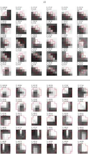
neighbors. Each pixel takes the difference of these intensities (the gradient) and mul-tiplies them to generate precursors of the terms in the characteristic equation C. A sum of these values is approximated by resistive grids shared among all pixels. Each pixel then draws values from the resistive grids as inputs to its selection circuit. The selection circuit within each pixel produces a binary value to indicate whether a feature is centered on that pixel. . . 34 2.7 A sample image used to generate the features shown in fig. 2.8 . . . 42 2.8 The 30 best features detected by a 3x3 Kanade feature detector (bottom) and the
Orthogonal Gradient Detector (top) in the image from fig. 2.7. The red outline indicates pixels considered by each detector. Values above each patch are the “featureness” of that image patch, that is, the value that is thresholded to determine whether to classify the patch as a feature. For the 3x3 Kanade detector, FK is the smaller of
the eigenvaluesλ. For the OGD, FO is the smaller of the gradient values. Both FK
andFO are normalized to range between 0 and 100 within the image. Implications of
differences between the detectors are discussed in the text and in figs. 2.10–2.16. . . . 43 2.9 Example of detecting local motion. To find the local motion, the 3×3 image patch
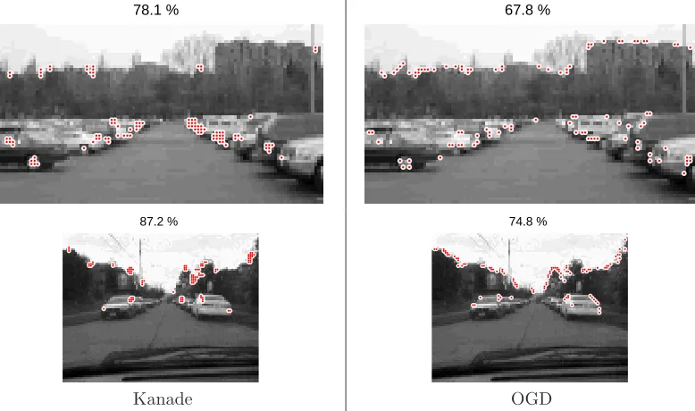
2.10 This synthetic image shows some of the fundamental differences between the Kanade detector and the OGD. Each red dot marks one feature. The percentages listed above the images indicate the fraction of features for which local motion was correctly esti-mated, as described in the text. Note that the Kanade detector responds strongly to high-contrast areas of local structure. The OGD selects both those areas and also sev-eral edges, which it confuses for a series of salient features. However, enough variation exists at those edges for the percentage of correctly tracked features to be only slightly lower for the OGD. . . 45 2.11 In images with much structure and thus easily-trackable points, both the Kanade and
the OGD perform similarly. There are few diagonal lines and highly textured areas that would confuse the OGD in a manner manageable by the Kanade detector. . . . 45 2.12 Many city scenes contain simple structures, such as cars, and the performance difference
between the two detectors seen here is typical. . . 46 2.13 In this image, the diagonal lane marker vastly reduces the effectiveness of the OGD.
Because the OGD responds to diagonal lines, the chosen “features” along the edges of the line provide poor locations for motion estimation and thus incorrect local motion estimates. . . 46 2.14 Many highly textured images result in local motion estimates of similar quality,
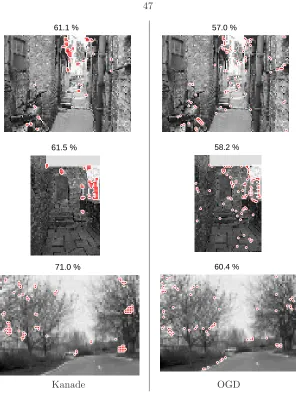
sur-prisingly. While one might expect that the ability of the Kanade detector to detect structure would be especially critical in such images, in practice it turns out that local structure provide a small advantage over simply finding very high-contrast spots within the image. . . 47 2.15 In images with relatively high frequency structure, the Kanade detector significantly
outperforms the OGD. The backs of the chairs have spatial structure that is picked out well by the Kanade detector. For the OGD, on the other hand, each chair is simply a highly textured area with one spot no more salient than another. It is unable to consistently recognize the same features. . . 47 2.16 An unusual example wherein the OGD performs better than the Kanade detector. The
3.1 Layout for mismatch reduction. Left: Common-centroid layout improves matching be-tween nearby transistors. Consider what happens if a linear doping gradient exists on the chip such that the left side of the figure receives a lower dopant concentration. The transistor formed by the left side of D2 and S will have low doping. The transistor formed by the right side of D2 and S will have higher doping. If the doping is linear, the doping of the left channel will differ from that in the center of the structure by an amount equal and opposite to the amount of change in the right channel of that transistor. Their average value remains constant and equal to that of the transistor between S and D1. Thus, the two transistors (D1 to S, and D2 to S) will be matched. Right: Photolithographically invariant layout compensates for non-vertical dopant im-plantation, not uncommon in drain/source implants. If dopants are implanted from a source to the right of the shown transistor, each gate can cast a shadow wherein fewer ions are implanted to the left of the gate. This results in capacitance mismatch between CGS andCGD. Laying out each transistor as two oppositely oriented transistors, the
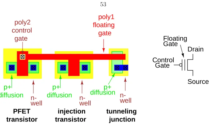
effect of the implant angle is matched. . . 50 3.2 Cross section of a floating gate transistor (not to scale). . . 52 3.3 NMOS floating gate transistor, shown with structures for injection and tunneling. The
circuit symbol for the NFET floating gate transistor is shown on the right. . . 52 3.4 PMOS floating gate transistor, shown with structures for injection and tunneling. The
circuit symbol for the PFET floating gate transistor is shown on the right. . . 53 3.5 Gate oxide thickness as a function of time. The date is extracted from two books (by
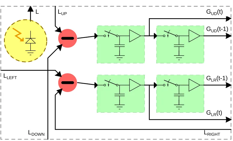
Brown [64] and by Sharma), a talk by Gordon Moore (Intel), and the International Technology Roadmap for Semiconductors [1]. LOP = “Low Operating Power.” MPU = “Microprocessor Unit,” referring to high-performance digital logic. NVM = “Non-Volatile Memory.” While the exact values are open to discussion based on whether one prefers to note cutting edge technology in development or well-established processes, we can note some trends. First, as lithographic transistor dimensions are scaled down every year, oxide thicknesses also decrease monotonically. Second, the oxide thicknesses for non-volatile memories plateau at about 70˚A. . . 54 3.6 Conceptual block diagram of a single pixel. Ldenotes the photoreceptor output in
re-sponse to the sensed light intensity. The analogous rere-sponses of the pixel’s neighbors are denoted asLU P,LDOW N,LLEF T, andLRIGHT. The outputs of the difference circuits
are stored in sample-and-hold circuits. Since they represent the vertical (Up-Down) and horizontal (Left-Right) gradients, they are denoted asGU D andGLR, respectively.
The pixel stores gradient values for the current time step asGU D(t) and GLR(t); and
3.7 Block diagram of a single pixel, as implemented. To reduce layout area, only one difference circuit is used. Switches are used to select between inputs (either horizontal or vertical) and which sample-and-hold should store the difference. . . 56 3.8 The basic topology of an integrating photodiode sensor. The capacitance of the NFET
and PFET instantiations is provided by the inherent capacitance of the photodiode. . 57 3.9 Simple logarithmic sensors based on photodiodes. . . 58 3.10 Logarithmic photoreceptors with feedback. The topology shown in A was used by Ni
et al. [58]. Landolt et al. [50] chose topology B after analysis of all three topologies for bandwidth and damping. Delbr¨uck et al. [21] implemented a topology similar to C. The transconductance of the amplifier is denoted bygm. Most simply, the amplifier
can be implemented as a single transistor with node aattached to the gate and the source and drain connected to node b and ground. The output resistance is denoted bygb. When the circuit is not driving a resistive load,gb arises from the amplifier. . 59
3.11 I uniformly illuminated a linear array of 16 logarithmic photoreceptors. As I swept the magnitude of the illumination, the voltage output of the photoreceptors changed with the log of the light intensity, as expected. . . 60 3.12 Logarithmic photoreceptor, with and without a floating gate for reducing mismatch,
both fabricated in the same 0.35µm process. A: A basic logarithmic photoreceptor. B: The response of 16 non-programmable logarithmic photoreceptors to a uniformly illu-minated LCD monitor. C: The response of 16 floating-gate logarithmic photoreceptors to the same stimulus. D: A floating-gate logarithmic photoreceptor. . . 61 3.13 Floating-gate photoreceptor output voltage as a function of the illumination for a 16×16
array. Bars show the standard deviation of the pixel values at each point. Left: Data as a function of the LCD monitor value, in units used by the monitor. Right: The same data with the x-axis converted to light intensity, based on data from a light meter. 62 3.14 Overview of the difference circuit diff. Both the intermediate output Idiff and the
final output Vdiff are proportional to the difference of the inputs (V2 −V1). In the context of the feature detection chip,V1andV2come from neighboring photodetectors such thatVdiff is proportional to either the vertical or horizontal light intensity gradient. 63 3.15 Cartoon illustrating the concepts of “gain” and “offset” as applied to thediffcircuit.
3.17 The topology of the fabricated difference circuit. Note that P1 and P3 are twice as wide as P2 and P4 to build an offset into each input differential pair, as discussed in
the text. . . 66
3.18 Mismatch in the difference circuit can be represented as offsets in the threshold voltages of the input PFETs. The threshold voltage shifts are denoted byVM1,VM2,VM3, and VM4. . . 67
3.19 Simulation results for programming the difference circuit to remove mismatch. The black line shows initial simulation with no mismatch. Red line shows circuit output with error added to some of the inputs to model mismatch. Calibration phase 1: The dotted blue line corresponds to output after offset removal by adjustingVf gρ and thus the ratio between Iρ andIref. Calibration phase 2: The green line is current output after adjusting bothVf gρandVf gγ to correct offset and gain, respectively. The gain is proportional toIγ, which is controlled byVf gγ. . . 70
3.20 The current-to-voltage circuit integrates current onto a capacitor for a prespecified time interval. The resulting voltage is buffered and sampled by a sample-and-hold (S/H) which outputs a voltage that is linearly proportional to the input current. . . 71
3.21 Injection to the floating gate fgρchanges the offset of the difference current output. Left and center: Measured data for two distinct difference circuits. Before programming, the data is offset due to mismatch (red circles). After programming, the transfer function is calibrated to cross the origin (black squares). Unmarked cyan lines indicate intermediate values during programming. Note that the gain is slightly affected by programming fgρin both examples. Right: Cartoon of concept. . . 72
3.22 Sweeping the floating gate voltage Vf gγ changes the bias currentIγ in the difference circuit, and thus the magnitude of the output current, allowing calibration of thegain. Left: Measured data. Right: Cartoon of concept. . . 72
3.23 Output of difference circuit to blank screen and edge stimuli. . . 73
3.24 Output of difference circuit to corners. . . 74
3.25 Block diagram of the sample-and-hold circuit. . . 75
3.26 Transistor schematic of the sample-and-hold circuit. . . 75
3.27 Generating a simultaneous pair of clock waveforms. Note that the circuit contains two identical stages in series. The delay betweenclkandN clkafter the first stage is 14.6ps (simulated). The delay after the second stage is 0.8ps (simulated). In comparison, one inverter delay is about 134ps. . . 76
3.29 Measured data for a single sample and hold circuit. Left: Entire operating range.
Center: Zoomed in near 2.5V.Right: Zoomed in near 4.4V. The input Vrst is swept
(x-axis). The blue lines indicate the output of the sample-and-hold circuit in sample mode. The red line indicates the output after the transition to hold mode. As can be seen from this figure, the functional range of the circuit is from 2.45V to 4.42V. . . . 79 3.30 Effect of sweepingVncas on the size of the pedestal withVpcas= 2.2V. . . 80
3.31 Effect of sweepingVpcas on the size of the pedestal withVncas= 1.0V. . . 80
3.32 Left: The saliency circuit. If the input gradient valueVgradX (or VgradY) exceeds the
boundaries of the programmed thresholds VthL and VthH, the intermediate saliency
valuenSALX (or nSALY) will be zero. If bothnSALX and nSALY are zero, then
SAL will be high. Thus, the circuit will be deemed salient only if both the X and Y gradients exceed the thresholds. Right: Subcircuits to compare the gradient values to preset thresholds. The Memory Cells [30] are programmed by tunneling and injection to store the thresholds. . . 81 3.33 Photoreceptor and supporting circuitry. Vf g is the voltage on the floating gate, which
allows adjustment of the DC offset of the photoreceptor output. The PFET source-follower is used within each pixel to buffer the sensitive photodiode node. An on-chip bias generator produces the voltage Vf ol which is shared among all pixels. An
externally generated bias currentIf bias provides a reference to the bias generator. The
power supply is broken up into VddA, VddB, and VddC to facilitate discrimination of
the different ways in which subcircuits are affected by their power supplies. The three supplies can be independently controlled in the fabricated chip and its test board. . . 83 3.34 Photoreceptor with NFET follower for reduced sensitivity to power supply fluctuations
(not fabricated). . . 86 3.35 Measured data showing dependence of photoreceptor on the power supply voltage,
directly on the left and including impacts on other biases on the right. Cyan lines show individual curves for each pixel in an 8x8 block. Black line and circles show mean values for those 64 pixels. The power supply can affect circuit response in several places. To separate the magnitudes of fluctuations at different points in the circuit, different biasing configurations were tried wherein only some of the supply rails and biases were swept. Shown here are the two most extreme situations. On the left, only VddA is swept. On the right, four parameters are swept simultaneously: VddA (the
photoreceptor power supply), VddB (the follower power supply), Vphn (photoreceptor
bias), andIf ol which controls the follower bias. Note the different scales on the y axis.
3.36 To assess the effect of power supply variation on the photoreceptor, I swept the power supply both on the fabricated chip and in simulation. The results are similar, confirming the accuracy of my simulations. I sweptVphnas if it were generated by a resistive divider
betweenVddAand ground, since that was my default configuration for generatingVphn.
That is, a 10% reduction inVddAwould correspond to a 10% reduction in Vphn when
both were swept. An on-chip bias generator creates the follower bias voltageVf ol. Vf ol
is swept by tying the power supply for the off-chip resistor sourcing If bias to VddA.
When VddB was swept, it was tied directly to VddA and left at 5V when not swept.
Note that the values listed in the table are the change on Vout for a 500mV change
on VddA, which is much greater than the actual power supply noise that we should
reasonably expect. Voltages are defined as shown in fig. 3.33. . . 88 3.37 Effects of power supply fluctuations on the difference circuit (simulation). Left: The
slope presented here is a measure of the change in output currentIdif f as a function
of the differential inputV1−V2. It is directly proportional to the gain, as introduced in fig. 3.15. Right: The offset is the inputV1−V2 necessary to produce a zero output current, also introduced in fig. 3.15. The curves in each plot correspond to sweeping a different set of biases. SinceVbiasandVrefmay be generated by on-chip bias generators,
their dependence onVddmay vary. On the currently fabricated chip, they are provided
by independent power supplies and thus independent of Vdd inasmuch as laboratory
instruments are independent. Blue
: Sweep of Vdd, with all other biases constant
with respect to ground. Red triangles: Sweep of Vdd and Vbias, whereVdd−Vbias is
constant. Magenta squares: Sweep of Vdd, Vbias, and Vref, where both (Vdd−Vbias)
and (Vdd−Vref) are constant. . . 89
3.39 Left: Finding the threshold voltage relies on extrapolating transistor curves to find where the transition between subthreshold and above threshold operation occurs. Since these curves are shifted by temperature, discussion of how the threshold voltage shift impacts the physics of the device inherently becomes circular. Solid black curves show measured transistor current (courtesy of Jeremy Holleman). Dashed red and dotted blue curves rescale the measured data to show how it would be different ifµ∝T−3/2
varied in above-threshold operation. Right: The assumption that transistor current varies primarily with µis consistent with the results of physical simulations in Atlas (courtesy of Jaideep Mavoori). Lines show results of physical simulation for several temperatures. ×s indicate values resulting from rescaling the green line for T=300K as ifµ∝T−3/2, discarding any other sources of variation with temperature. . . 94 3.40 Physical simulations in Atlas show temperature dependence of transistor current.
Be-low threshold, current increases with temperature. Above threshold, the opposite re-lationship holds, such that current decreases with temperature. The point where the relationship inverts is called thetemperature compensation point (TCP). The same data is plotted on a log scale (left) and linear scale (right). Left: Below threshold. The up-ward shift (on the log scale) for successively higher temperatures can be characterized by the terme−φ0/kT. The decreasing slope with temperature can be explained by the term eqVgskT . Note that the simulated transistor was not saturated, so the
tempera-ture dependence of the Early effect term would decrease the current as a function of temperature by about 0.5% over the temperature range shown. Right: Above threshold. 95 3.41 NFET gate capacitance as a function of the gate–source voltage Vgs, from an EKV
model simulation. As described in the text, the capacitance decreases as the channel becomes more strongly depleted due to increasing gate voltage in subthreshold. When the device reaches threshold, the channel inverts and gate capacitance returns to its maximum, proportional toox·A/tox, whereAis the area of the device. . . 96
3.42 Left: The band diagram of an MIS diode. A positive bias applied on the gate causes the bands to bend downwards. When the conduction bandEc reaches the Fermi levelEF,
as shown here, the device is at threshold. The potential difference between the intrinsic and Fermi levels is defined by qφb ≡Ei−EF. The level of the conduction band EC
at the silicon-oxide interface defines the surface potential,φs. Right: As temperature
increases, the intrinsic carrier concentration increases. This causes the Fermi levelEF
to shift closer to Ei. The amount of band-bending necessary for EC to reach EF is
thus reduced, which corresponds to a decreased threshold voltage for the device. . . . 97 3.43 Change in gate capacitance for an n-channel transistor, as estimated from the EKV
3.44 Cadence simulations of the effect of temperature on photoreceptor output, assuming constantVf g. The general trend is that the photoreceptor output voltage increases by
1.835 mV/◦C for Vph and 1.113 mV/◦C forVout. Top left: Unbuffered photoreceptor
output (Vph) as a function of photocurrent for several temperatures. Top right:
Pho-toreceptor output buffered by a source-follower (Vout) as a function of photocurrent
for several temperatures. Bottom left: For a single photocurrent, unbuffered photore-ceptor output as a function of temperature. Bottom right: For a single photocurrent, buffered photoreceptor output as a function of temperature. . . 99 3.45 Cadence simulation of temperature effects on difference circuit. . . 102 3.46 Cadence simulation of temperature effect on bias current in the difference circuit. . . 103
A.1 A differential pair . . . 116
B.1 Layout area (in µm2) of a digital multiplier (left) and adder (right) as a function of speed. . . 119 B.2 Layout area (in µm2) of a digital multiplier (left) and adder (right) as a function of
List of Tables
3.1 Overview of some previous implementations of logarithmic CMOS sensors with reduced fixed-pattern noise (FPN). . . 61
Chapter 1
Introduction
Self-motion estimation is a vital problem for autonomous robots. To move through an environment effectively and without harm to oneself, a robot must possess some means of estimating its motion relative to surrounding objects. The problem is constrained by the need for real-time operation, a compact solution that constitutes only a fraction of the robot’s payload, and limited power avail-ability. This thesis presents part of the solution, specifically circuits for image and feature detection, to be followed by digital processing for ego motion estimation. The system comprises a chip con-taining a photodetector array as well as local processing circuitry within the array. For each pixel, the chip outputs the detected light intensity, horizontal and vertical gradients at the current and previous time steps, and whether or not the pixel is centered on a salient feature. Off-chip digital postprocessing can be used to estimate the local 2-D motion at each salient pixel. The local motion estimate then can be combined to calculate the 3-D motion of the imager relative to its environment. The postprocessing could easily be integrated onto the photo-sensing chip.
1.1
Vision for Motion Estimation
A variety of sensory modalities can be used for motion estimation. The choice of one over another depends on the system and the environment in which it is to operate. For tracking absolute self motion, inertial sensors that directly measure linear or rotational acceleration may be the right answer. Inertial sensors may be implemented as MEMS (Micro Electro-Mechanical Systems), while necessary postprocessing can be embedded in either an analog or a digital circuit fabricated in CMOS (Complementary Metal-Oxide-Semiconductor). Because of the difficulties of integrating MEMS and CMOS on the same die, such integration can be solved by either a two-chip solution, or a more expensive bonding of the two dies into one package. Depending on the noise levels within the sensor and required precision of measurement, the sensor may need to be recalibrated to known landmarks by some secondary sensing scheme.
and motion of nearby objects. This is particularly true in the case of airborne or underwater robots, where motion relative to their medium may be different from the absolute motion measured by an inertial sensor. Also, inertial sensors cannot be extended to assess the approach of another object or vehicle. Medium- and long-distance sensors that are able to deal with such tasks include both vision sensors that detect light reflected by objects in the environment, and active sensors that emit and detect their own signal such as laser range finders. Of these, the preferred choice is dependent on the application. Benefits of active sensors include some independence from ambient lighting conditions. Active sensors are not appropriate for environments where stealth is important, since the signal emissions could be detected by other agents. Active sensors also require additional power to emit their signal. Power constraints thus limit the range of an active sensor since it becomes impractical to illuminate too distant an object.
Therefore, a number of applications are best served by passive vision sensors, for example, an autonomous mobile robot with limited power resources and the need to detect both ego-motion and motion or location of nearby objects. Although the system presented here does not calculate the trajectories of other moving objects, it provides a basis to do so in the future.
1.2
Custom Single-Chip Approach
Image processing systems, whether human, animal, or robotic, extract meaning from the world by building up an internal representation. Most such systems do this by hierarchically merging the information from individual photodetectors into simple features and processing those simple features to extract more abstract information. The simple features may be spatial, such as edges, salient local contrast patterns, or patches of color. They may be temporal, such as patches of pixels whose intensity changed significantly over some time interval. The type of simple features and the number of processing steps between these features and the desired abstract information will vary with the application and medium of implementation.
real-time control as they move through their surroundings. Likewise, the emerging field of ubiquitous computing desires small, cheap, low-power processors for embedding throughout an environment. In both these scenarios, embedding the most expensive computation in a specialized, lower-power processor can be a big win. Since the computation of features is a local computation, it lends itself well to a focal-plane implementation where the computational elements are located within the pixel array and process information in parallel.
1.3
Analog versus Digital Processing
The output of a pixel array requires substantial processing before a useful quantity like speed or direction of motion can be extracted. People argue whether analog or digital systems are better suited for information processing [68]. The underlying and more general question iswhen(or if ever) during signal processing should one switch from the analog to the digital domain. At a macroscopic scale, variables of interest are fundamentally continuous: volume or frequency of a sound, velocity, acceleration, light intensity1 or wavelength, force, etc. Likewise, the sensors designed to measure these variables are analog. Proponents of digital systems cannot argue against the inherent existence of analog signals, but rather, for the conversion from analog to digital to occur as early as possible in the processing scheme.
The merits of analog and digital cause them each to be preferable in different situations. Since, typically, digital platforms can be reprogrammed more easily than custom analog chips, digital processing is a reasonable choice for parts of a system that may need to be modified, either as an algorithm is developed or refined or to accommodate a different set of requirements. On the other hand, analog processing is appropriate for initial amplification and filtering of a signal. It is well-suited to performing well-understood transformations known to be useful and unlikely to require modification. Analog implementation may result in a more compact and power efficient system, although the design process is more demanding. When applied to arrays of elements, due to connectivity limitations, analog processing tends to befit local computation and is less suitable for global analyses. The precision of the computation is limited by noise and distortion in analog systems, and by the number of bits chosen in a digital implementation. Increasing the number of bits requires more silicon area or processing time, and requires more power.
In general, then, local early processing that needs to be applied to every element of an array lends itself well to analog processing. If high precision is not required and the designer finds a means
1Technically, if we delve down to the level of quanta of light, we will be forced to admit the non-continuous,
to embody the desired computation in a compact analog circuit, the resulting circuit may be faster (due to its parallelism), more compact, and less power hungry than an equivalent digital version. These traits describe exactly the vision application at hand. Detecting local features is a time-tested first step in many algorithms (e.g., [12, 29, 36, 43, 57, 70, 71, 72, 84]) so the loss of flexibility to easily reprogram that step of the computation is not likely to impact the final system.
1.4
Motion Estimation Algorithms
Several approaches to motion estimation exist in the literature. I will give a brief overview of some popular algorithms. The gradient model and energy models compute a value at each image location that combines information about how the image varies in space (the gradient) and time. The motion estimate is computed directly from the image. Token-based motion detectors select salient “tokens” or “features” and track these in time. The motion estimate is computed based on information about the location of these tokens, with the token detection as an intermediate step. This thesis uses a token-based algorithm.
Oftentimes, image detection is not continuous. Instead, the system acquires “frames” wherein a “frame” contains intensity information for one instant in time, and frames are typically separated by a constant time interval. Descriptions of the algorithms within this section use this notion of frames since, in practice, image processing algorithms are often implemented in this temporally discontinuous manner.
1.4.1
The Basic Gradient Model for Motion Estimation
Gradient-based motion methods are based on the approximation that local 2-D velocity can be calculated from the local gradient and from the change in local intensity over time [28, 41, 44, 45]. The basic gradient model computes the ratio of the temporal flicker and the spatial flicker, as illustrated in fig. 1.1. The temporal flicker is δI
δt, pictorially represented as (T+−T−). The spatial
flicker is δI
δx, pictorially represented as (S+−S−).
We can derive the mathematical expressions for the model as follows. For a linear image, denote the image intensity at locationxand timetbyI(x, t). Assuming that the brightness of image points does not change during the motion (i.e.δI/δt= 0), the image subjected to a translation at velocity vfor a time intervalτ is denoted byI(x−vτ, t+τ). By the chain rule of basic calculus we then can write the 1-D velocity as:
δx δt =−
δI δt ·
δx δI
1.4.2
Energy Models for Motion Estimation
Energy-based motion detectors (e.g. [3, 14, 38, 39, 78]) merge spatial and temporal information to compute the motion energy, as shown in fig 1.1. These models look for patterns inx-y-t space; a velocity corresponds to orientation in this space. In contrast to the basic gradient model which calculates speed directly (e.g., in pixels per frame), the output of these detectors indicates how closely the stimulus matches the tuned detector. A nice review of the basics of spatio-temporal motion detection can be found in [45].
The inspiration behind some of these models has been biologically driven. The Adelson-Bergen model [3] and that of Watson and Ahumada [78] are consistent with the electrophysiology of motion perception in primate cortical complex cells. The Hassenstein-Reichardt [38] correlation motion detector accurately models the optomotor response in flies and was later extended by van Santen and Sperling [76, 77] to human motion perception. The Barlow-Levick [8] mechanism describes direction selectivity in the rabbit retina.
Fig. 1.1 illustrates two of these models, the Hassenstein-Reichardt [38] and the Adelson-Bergen [3]. The Reichardt correlation motion model computes a correlation between two patches in time-space (L0×L1) and subtracts the result from the correlation between two other patches (R0×R1). For example, consider a high-contrast feature that stimulatesR0. If it moves in space and time to stim-ulateR1, the correlation (R0×R1) will be high, and the overall response will be large. The pair of detectors L0 and L1 will respond to motion in the opposite direction fromR0 andR1. Thus, the sign of the difference of the final output (R0×R1)−(L0×L1) will indicate direction. The detector is velocity-tuned. The Adelson-Bergen model uses filter kernels oriented in space-time detect the presence of motion in a particular direction [78]. A black and white bar moving rightward will cause a large response in R = R+−R−. Conversely, the same bar moving leftward will activate L=L+−L−. Like the Reichardt model, the final output of the Adelson-Bergen motion detector is a comparison of motion in the rightward and leftward directions. In the Adelson-Bergen model, pairs of filters in quadrature phase are applied to images and the outputs are squared and added. The use of filters in quadrature phase ensures a response to both edge and bar stimuli. The squaring operation results in indifference to the sign of the changes.
1.4.3
The Kanade Motion Detector
as:
L(x, t) = L(x+d, t +τ) (1.1)
whereL(x, t) is an image patch at locationxand at timet,dis the displacement (motion) between frames, andτ is the time between frames. The full formulation provides an algorithm for detecting salient features that are easily trackable, where trackability is rigorously defined by minimizing the error between the constraint in eqn. 1.1 and the actual change in image patches. I describe the mathematics in more detail in sec. 2.2. The Kanade algorithm provides a means of estimating the displacementdby inverting a matrix and multiplying it by a vector (see eqns. 2.3 and 2.4).
The Kanade detector and variations upon it are popular in vision literature. However, the com-putations are difficult to implement directly with analog circuits and computationally expensive in digital post-processing. Sec. 2.3.2 describes the difficulties encountered by Pesavento [61] in building analog circuits that were ultimately crippled by mismatch [62], while in sec. 2.3.5 I explain why the very non-linear nature of Pesavento’s circuits would make it very difficult to fix his mismatch problems. Digital implementations require a sequence of computationally expensive operations. The analog image data first needs to be digitized by an A/D (Analog to Digital converter). The Kanade feature computation itself requires 3 multiplications to calculate the characteristic matrix, plus an-other two multiplications and one subtraction to calculate the featureness value, plus a thresholding operation (see sec. 2.2 and 2.4.3). Floating-point multiplications are especially expensive and in some computer architectures may require multiple clock cycles to compute. Even an integer mul-tiplier requires approximately 40 times more layout area than a comparable analog mulmul-tiplier with floating gates for mismatch compensation (see sec. B).
1.4.4
Token-Based Motion Estimation
Token-based (or feature-based) motion detectors [12, 33, 57, 65, 82, 85] compute local motion by selecting salient “tokens” or “features” to track between frames. They compare a target image patch in one frame to potential match candidates in another frame and select the closest match. This match provides an estimate of where the image patch moved between the frames. Attempts are made to perform correlations more selectively since performing a correlation between every pixel’s neighborhood and every other pixel’s neighborhood in another frame would be unmanageably expensive.
additions, andN ·(K−1) comparisons. We also need to store in memory the N2 floating-point results from each multiplication. A modern 2 GFLOPS (billion floating-point operations per second) processor could process images of up to 38×39 pixels at a frame rate of 30Hz. Token-based methods improve throughput and thus allow processing larger images.
Token-based correlation methods restrict correlations to patches centered on tokens (aka fea-tures), where “tokens” are defined [75] as image patches that are easy to recognize from frame to frame at multiple points in time. Computational resources thus are not wasted on image patches that are unlikely to be correctly and uniquely tracked, such as areas of low contrast.
1.4.5
Our Implementation
In all these motion estimation methods, some local calculation is repeated over the entire imaging array. If a multi-purpose digital computer is used, it implements these massively parallel operations serially. These low-level repeated calculations are thus a major hindrance in the implementation of real-time solutions [11, 32, 48].
The system presented herein implements a token-based correlation algorithm. I considered using Kanade features, extending the work of Pesavento [61], but correcting for mismatch in a circuit as complex as that necessary to calculate Kanade features is prohibitively expensive. Instead, the hardware embodies a simpler feature detector introduced in sec. 2.4. Each pixel measures the local light intensity. Based on its neighbors’ outputs, it also calculates the local horizontal and vertical gradients. Each pixel is deemed to be centered on a salient feature if both the x-gradient and y-gradient are of sufficiently large magnitude. For those pixels deemed salient, a local search compares each given pixel to its neighbors to determine which neighbor most likely viewed that same feature at a previous time step. The gradient calculation is performed by an analog circuit embedded within every pixel. When a pixel is selected to be read out, its outputs are also directed to a saliency circuit (unique on the chip). The local search for a match in a previous frame is controlled by digital processing external to the chip. Thus, a compromise is struck to take advantage of the merits of both the digital and analog domains. The simple and local calculation is efficiently implemented on the same chip as the photo-sensing array, parallelizing a huge computational task and vastly reducing the amount of data to transmit off chip. Calculations requiring more complex addressing, namely the search for a most-similar neighbor, are performed by digital circuitry.
1.5
Motion Estimation in Hardware
information processing (often in the analog domain) on the same custom chip.
Multi-chip designs benefit from flexibility to reprogram the system. However, the serial nature of CCD readout and typical digital processor operation is poorly matched to the dramatically parallel nature of the image processing problem. Real time implementations thus rely on clever optimizations and modern hardware with fast clock rates. For a demonstration or application where size and power are not of concern, this is very appropriate. The target application of this thesis, namely mobile robotics, has more stringent requirements.
Monolithic implementations often parallelize the low-level image processing by including some of it within each pixel. Alternately, the processing is done by circuitry at the edges of the photodetector array but still on the same chip. If done well, focal-plane processing can reduce the amount of repetitive local computation required off-chip, and can also reduce the amount of data that must be transferred from one chip to another. Unfortunately, many previous single-chip designs emphasized biological inspiration rather than motivating functional reasons for design decisions, showed test data only for synthetic bar stimuli, failed to discuss the effects of using natural stimuli, and/or used a communication scheme (Address Event Representation, aka. “AER”) that has limited application to larger arrays than those built on the demo chips.
However, it is more edifying to focus on previous work that has chosen similar design priorities as this thesis than to rebuff those whose authors apparently had different priorities. The following pieces of work are most closely related to the work of this thesis. Fiore et al. [32] and Benedetti and Perona [11] both implemented in hardware motion algorithms based on the Tomasi-Kanade feature tracking algorithm [75]. The central algorithm of this thesis derives from the same source as theirs. Pesavento [61] implemented the Tomasi-Kanade detection algorithm on a single chip, but did not attempt to extend the system to complete a higher level task. D´ıaz et al. [23] implemented a gradient optical flow algorithm (in contrast to feature tracking), also on an FPGA.
Benedetti and Perona [11] developed some simplifications to reduce the computational complex-ity and facilitate real-time implementation. Benedetti’s Field Programmable Gate Array (FPGA) implementation did not perform feature tracking nor motion estimation; it only detected Tomasi-Kanade features. The interesting aspect of Benedetti’s work was that it showcased his system of multiple FPGAs. This is a worthwhile technique for solving problems too complex for a single FPGA. What is more relevant to this thesis is that the choice of feature detection as a represen-tative task underscores the high demands of early vision processing and exemplifies the difficulty of accommodating an inherently parallel computation by an architecture that is itself not equally parallel.
feature extraction accounted for 93.5% of the computational cycles. Parallelization of the feature extraction, as recommended in this thesis, is a worthwhile improvement on the design [31] because it decreases the computational demands placed on the digital postprocessor. This frees the multi-purpose digital hardware for use in other tasks, allows the use of a smaller cheaper digital processor, and makes possible the integration of digital postprocessing as an Application-Specific Integrated Circuit (ASIC) on the same die as the image sensing and feature extraction. It also permits motion estimation from a larger imaging array.
Pesavento’s chip [61] successfully implemented the Tomasi-Kanade feature detector in local ana-log circuits embedded within every pixel. While the individual feature detectors worked well, it was impossible to find bias settings where an acceptably large percentage of the feature detectors would all function. Mismatch between elements rendered the array as a whole unusable [62] because the array elements had such dramatically different operating characteristics at any single bias setting.
D´ıaz et al. [23] implement the Lucas and Kanade [53] gradient optical flow algorithm in an FPGA. D´ıaz provides tables that allow an estimate of the number of gates used and thus the silicon area of the FPGA. If that same area of silicon were used for an analog pixel array, an imager of similar resolution performing the same calculation could be built but without the frame rate limitation of 30Hz. That is, the all-analog version using the same silicon area could run much faster.
This thesis presents a chip that is similar at a functional level to that of Pesavento, in that it implements feature detection within every pixel. However, mismatch is compensated by integrated programmable floating gates. The circuits have been completely redesigned due to this constraint. The chip is then combined with a digital postprocessor to extend the system to one akin to that of Fiore. The system presented here is more appropriate for mobile robotics applications than that of Fiore because it is, in principle, more compact and less power hungry. It is also easily scalable to larger array sizes simply by making the custom pixel array bigger, with minimal additional demands on the digital processor.
1.6
Mismatch Between Array Elements
Mismatch between devices has been a critical barrier to producing truly useful arrays of local pro-cessing elements. Imperfections in chip manufacturing result in circuit elements which are not quite identical. These disparities can render arrays of circuits unusable [62] when the array elements operate too differently. Standard approaches to mismatch reduction, such as using larger devices, surrounding critical devices with non-functional dummies, or mismatch invariant layout (sec. 3.1.2), require too much silicon area to be practical for embedding in every single element of an array.
as for any array. Additionally, the proportional change in current due to a given threshold offset may be greater for a transistor in subthreshold than for the same device above threshold, since subthreshold transistors display an exponential relationship between current and voltage while above-threshold transistors exhibit a square relationship. Mismatch has limited application of designs using subthreshold transistors, possibly more than any other factor [20].
The problem of mismatch is pronounced in analog focal plane processing arrays due to their use of logarithmic photodetectors. Integrating photoreceptors, which reset a photodiode and sample it some time later, are affected primarily by mismatch between the photodiodes. In modern high-quality processes, this mismatch is low enough to be acceptable for many applications. Measurements in 1.2µm and 2.0µm processes [46] indicate less than 2% mismatch between photodiodes. Unfor-tunately, because they are sampled, integrating photoreceptors are not well-suited to continuous-time analog computation. In contrast, logarithmic photoreceptors output a continuous-continuous-time voltage in response to illumination. Logarithmic photoreceptors send the photocurrent generated by the photodiode through a transistor. The transistor is operated in subthreshold and thus performs a logarithmic compression on the signal. Logarithmic compression is analogous to human vision and extends the dynamic range of the photoreceptor far beyond that of a CCD camera [51] or a CMOS integrating photoreceptor. Mismatch in logarithmic photoreceptors results primarily from voltage threshold mismatch in the transistor that performs the logarithmic transformation, and the mis-match between transistors is larger than that between photodiodes. Fig. 3.11 illustrates the effects of mismatch on a small array of logarithmic photoreceptors. The shift in output voltage due to mis-match is of a magnitude comparable to that resulting from typical signals. Some sort of mismis-match correction, either within the photoreceptor array or in later processing, is critical to fabrication of functional logarithmic imagers [51, 61]. I present a modified photoreceptor with floating-gate mis-match compensation and compare it to a non-programmable photoreceptor in fig. 3.12. Sec. 3.3.5 quantifies the obvious improvement.
programmed once to permanently remove mismatch between the subcircuits into which they are embedded.
1.7
Beyond Preprocessing
This thesis presents a focal plane aVLSI (analog Very Large Scale Integration) chip specifically intended for integration into a system which accomplishes a useful task: ego motion estimation. Focal plane processing has existed for years. Many interesting vision preprocessors have risen out of this field [7, 15, 17, 27, 49, 52, 69, 79, 80, 81]. However, much of this prior work did not target a clearly defined application, or focused on some simple toy problem without a clearly defined path to deal with messier real-world problems. Keeping the end application in mind is critical to building components which will be truly expandable to real-world problems and have a practical interface.
Admittedly, the implementation of feature detection in analog circuitry takes away the flexibility to modify the feature detector itself. However, since the Kanade feature detector is widely regarded as a robust front end, it is unlikely that one would need to modify it. Being a local computation, it is ideally suited for local implementation in an analog circuit. However, the aggregation of local data into a global estimate is better done by a single digital circuit to succeed the fabricated analog chip.
Chapter 2
Feature Detection for Motion
Estimation
This chapter will focus on the algorithmic basis for a feature detector implemented in hardware, beginning with an overview of motion detection and culminating in a derivation of a feature de-tector appropriate for implementation in hardware. The highly repetitive nature of low-level image processing makes feature detection an ideal candidate for embedding in the circuitry of a custom chip, as discussed in chapter 1. However, a prior attempt at such an implementation [63] was de-bilitated by mismatch. To avoid this pitfall in my design, I modified the feature detector to allow incorporation of floating gates for mismatch reduction. This chapter includes simulations of the functionality of the implemented feature detector. Sec. 3.2 provides the implementation details of the circuits embodying my feature detector.
2.1
Motion Detection Overview
This section presents an overview of a motion estimation algorithm to provide background for un-derstanding the remainder of this chapter. I explain how feature detection fits into the broader application of motion estimation and outline the basic steps of motion estimation, the first of which is feature detection and the focus of the current chapter.
As illustrated in fig. 2.1, the motion estimation algorithm can be subdivided into three steps. The second and third steps occur outside the photoreceptor array, in my system in an off-chip postprocessor, with the option of implementation on the same chip. The image and feature data become available only at discrete time intervals, the length of which is determined by how long it takes to read out the array. Each complete chunk of analog data about the entire array is termed a “frame”.
Detect features
Estimate local motion
Estimate global motion
Figure 2.1: The motion estimation algorithm detects salient features within each image. It then estimates the local motion of each feature between successive frames. Based on these local motion vectors, it generates a global motion estimate.
2. Estimate local motion: For each detected feature, find the location to which it has moved in the next image frame. We assume a high frame rate relative to the speed of motion, so we need only search a local neighborhood of the feature to find its location one time step later. The vector pointing from the original feature location to the new location is the local motion vector for that feature.
3. Estimate global motion: Aggregate the local motion vectors to estimate a global motion vector that would have resulted in the local motions.
Poor feature
Poor feature
Good feature
low contrast aperture problem: Both vertical and similar neighborhood as horizontal gradients
image moves vertically. are large.
Figure 2.2: The images above show sample image patches that might be sensed by a 3x3 pixel grid. The central pixel (outlined in red) would use its neighborhood to determine a saliency value. The saliency value can be thresholded to decide whether the pixel is centered on a feature or not. Left: A patch of low contrast pixels. One low contrast patch is not uniquely different from a neighboring low contrast patch. Center: A high contrast edge. Motion parallel to the edge will result in little change to the central pixel’s neighborhood. Thus, an edge is a poor feature for tracking motions having a component parallel to that edge. This is termed the “aperture problem” since in principle a larger viewing area would include elements that could provide correct information about parallel motion. Right: A feature that has a high intensity gradient in both the vertical and the horizontal direction can be tracked regardless of the direction of motion.
2.2
Tomasi Kanade Features
Tomasi and Kanade [75] proposed a mathematically based description of a feature targeted at local motion estimation. Their definition fits the general overview presented in the previous section. The derivation begins by defining a feature as an image patch whose motion between two frames can be calculated, assuming translational motion with minimal other warping and assuming constant illumination. The resulting equations select as features those image patches having both large horizontal and large vertical intensity gradients, thus responding to corners and highly textured areas. They discard image patches having a large gradient along only one axis (edges) and low contrast areas. Tomasi-Kanade features have been used widely as the first step in algorithms for motion estimation.
Consider an image sequence L(x, t) where L denotes the light intensity, x = [xh, xv]T denotes
location within an image with xh the horizontal coordinate andxv the vertical coordinate, and t
denotes the time when that image occurred within the sequence. We can express the motion between successive frames by motion vectors such thatd(x, t) = [dh, dv]T expresses the motion at pointxat
time t, where dh is the direction and magnitude of horizontal motion and dv is the direction and
magnitude of vertical motion. Assuming a high frame rate (temporal sampling frequency), we can assume that small image regions undergo a geometric transformation due to motion of the camera or within the image, but the intensities of objects remain the same. Given these assumptions, the transformation from one frame to next over a time intervalτ can be expressed as:
L(x, t) = L(x+d, t +τ) (2.1)
The task of the motion estimation algorithm is then to find d for each of a set of automatically selected point features in a pair of successive image frames in the sequence.
However, eqn. 2.1 will not be satisfied exactly. The assumption of intensity constancy is not perfect so the light intensity of an image patchLmay change in a way not captured in eqn. 2.1, for example as objects move into a differently illuminated area. Points may also disappear or appear due to occlusion. Lastly, various sources of random noise exist, such as thermal noise within the sensor or distortion within the optics. Even the best estimate ofdwill not satisfy eqn. 2.1 perfectly. To estimated, then, find thedwhich minimizes the squared residual error:
=
W
[L(x+d, t +τ)−L(x, t)]2 (2.2)
from multiplier
to selection circuit
∆L(x,t) ∆xh
2
∼
W ∆L(∆xhx,t)2
Figure 2.4: The resistive grid in Pesavento’sDetector2, shown for C1,1. Similar grids exist for C1,2
andC2,2. Each node represented by a dot corresponds to one pixel. Resistors connect neighboring
pixels. The input to each node is the current output of a multiplier, in this case calculating the square of the horizontal gradient at that pixel. The output current flows through a resistor (drawn vertically) and to the selection circuit that determines whether or not a sufficiently salient feature exists that is centered on that pixel.
where pt is the threshold [61]. The selection circuit which calculated the quantity in eqn. 2.6 was
also implemented within each pixel.
Detector1 worked as expected. However, dedicating each 3x3 block of pixels to calculate only
one feature wastes space, especially since with three modified Gilbert multipliers in each pixel the pixels are rather large. In an improved design,Detector2, Pesavento used a two-dimensional diffusion network (resistive grid) to allow overlapping use of multiplier outputs (see fig. 2.4). The resistive grid performs a weighted summation of nearby currents, approximating the sum over W. For ex-ample, the summation ofC1,1at locationx= [xh, xv]T for a 3x3 pixel grid would be approximated as:
w1·C1,1(xh+ 1, xv−1) +w2·C1,1(xh, xv−1) +w3·C1,1(xh−1, xv−1)
WC1,1(xh, xv)≈+w4·C1,1(xh+ 1, xv) +w5·C1,1(xh, xv) +w6·C1,1(xh−1, xv)
+w7·C1,1(xh+ 1, xv+ 1) +w8·C1,1(xh, xv+ 1) +w9·C1,1(xh−1, xv+ 1)
In the original Kanade formulation, wi = 1 for alli. With a resistive grid,wi corresponding to a
nearby pixel has a larger value than one corresponding to a distant pixel. See fig 2.5 for a graphical representation.
The output currents of the resistive grids correspond toC1,1,C1,2, andC2,2. InDetector2, these
currents were input to a 47 transistor circuit which performed the thresholding of eqn. 2.6 and thus determined whether a feature was centered on the pixel or not.
The block diagram ofDetector2is shown in fig. 2.6.
2.3.2
Mismatch Problems in Pesavento’s Chip
all voltage bias settings configured as best possible, some pixels always indicated a feature, while others never flagged the presence of a feature even when surrounded by a highly salient image patch. Neither the multipliers nor other circuits within the pixel incorporated techniques for mismatch minimization.
Pesavento suspected that the mismatch was primarily due to mismatch within the three multi-pliers used to calculate the characteristic matrix. This is a plausible explanation. Small differences in threshold voltages could lead to significant errors when amplified by a multiplication operation.
My simulations of mismatch within a resistive grid suggest approximately 17% variation in the magnitude of the currents representingC1,1,C1,2, andC2,2when minimum size transistors are used,
8.5% with both length and width doubled (4x area), 4.4% with both length and width quadrupled (16x area). Thus, mismatch within the resistive grid would have impaired performance but should not have rendered the array useless.
Mismatch in the selection circuit has not been quantified by either simulations or measurements. However, this circuit may contribute as much to the mismatch problems as the multipliers. Since it relies on current mirrors for subtraction, small differences in threshold voltages would be reflected in the magnitudes of the currents. These currents are then multiplied, an operation performed by using subthreshold transistors cleverly. Mismatches in the voltage thresholds of these transistors would contribute further to mismatch errors. In short, the sources of mismatch in the modified Gilbert multipliers and mismatch in the selection circuit are similar. Further analysis would be required to tease apart the exact contribution of each.
2.3.3
Brief Overview of Floating Gates for Mismatch Reduction
We chose to use floating gate devices to reduce mismatch in these circuits, as explained in detail in sec. 3.1.2. Layout techniques are inappropriate or insufficient. Common-centroid layout can be used to reduce mismatch between nearby transistors but is not applicable to hundreds of transistors nor transistors on opposite ends of a large array. Photolithographically invariant layout would not improve matching sufficiently. Simply making larger devices requires too much area when we desire an array of identical circuits. Floating gate devices can be programmed permanently to modify the offset of a single transistor’s operating point so as to null the mismatch introduced by imperfections within the single circuit within which the transistor is embedded.
2.3.4
Reducing Circuit Mismatch in Non-linear Circuits
Any technique for mismatch correction should be applied judiciously, since some cost or performance trade-off is typically required. Floating gates require some additional layout area and increased operational complexity to initialize their values appropriately prior to operation. One way to consider the number of floating gates appropriate for a given circuit is to analyze the number of degrees of freedom that must be programmed to compensate for the major sources of mismatch.
Given a series of linear stages, only a single floating gate is necessary since the mismatch can be expressed as a single term requiring a correction with only one degree of freedom. Consider a series of circuits with linear transfer functionsHi(V) =Ai∗V, each introducing some mismatchVi, where
iis an index referring to each circuit. For an inputVin, the output of the series will then equalVout,
as expressed below. ˆ
Vout= An∗( An−1∗( An−2∗( ... ∗ A1∗Vin) ... ))) ideal
Vout=Vn+An∗(Vn−1+An−1∗(Vn−2+An−2∗( ... ∗(V1+A1∗Vin) ... ))) mismatched
Denote ideal output assuming no mismatch by ˆVoutand output including mismatch byVout. Simplify
and combine the two equations:
Vout = Vn+ (An∗Vn−1) + (An−1∗Vn−2) +...+ (A2∗V1) + ˆVout
= Vˆout+ N−1
n=1
An+1∗Vn
mismatch term
Since we are considering linear circuits, the gain terms,Ai, are scalars and thus the mismatch term
is a constant. Compensating for the mismatch requires adjusting the value of a single term. For every added degree of freedom in the circuits, we need to add one more floating gate to compensate. For example, a multiplier has two degrees of freedom which can be expressed as gain and offset:
Vout =Again∗(Vin1∗Vin2) +Vof f set
or equivalently, as offsets within each input term:
Vout = (Vin1+Vof f set1)∗(Vin2+Vof f set2)
to correct forVof f set1 andVof f set2, respectively. The choice should rest on ease of implementation,
that is, which expression can be better translated into a reasonable circuit topology.
Lastly, note that the mismatch in one circuit sometimes can be compensated in a succeeding circuit without introducing modifications beyond what already exists in that latter circuit. For example, a difference circuit has one degree of freedom, requiring one floating gate to correct. A multiplier has two degrees of freedom, requiring two floating gates. A multiplication of a difference, implemented as a difference circuit followed by a multiplier, has only two degrees of freedom. The mismatch in this combined circuit can then be compensated for by the two floating gates in the mul-tiplier, making a floating gate in the difference circuit extraneous. The outputs of these two circuits and of their combination are expressed in the table below. Note that the form of the expression for the mismatch in the combined circuit is the same as that of the multiplier alone. Offset mismatches are represented byVos1,Vos2, andVos3. Gain mismatches are denoted byAm1 andAm2. The inputs
to each circuit are expressed asVi1andVi2.
circuit: expression
difference: Vdif f = Vi1−Vi2+Vos3
multiplier: Vmult = (Vi1+Vos1)∗(Vi2+Vos2)
both: Vout = (Vdif f1+Vos1)∗(Vdif f2+


![Figure 3.5: Gate oxide thickness as a function of time. The date is extracted from two books (byBrown [64] and by Sharma), a talk by Gordon Moore (Intel), and the International Technologyscaled down every year, oxide thicknesses also decrease monotonically](https://thumb-us.123doks.com/thumbv2/123dok_us/1055199.1131839/58.612.201.450.86.301/thickness-function-extracted-international-technologyscaled-thicknesses-decrease-monotonically.webp)