IJEDR1403027
International Journal of Engineering Development and Research (www.ijedr.org)3061
Comparison of Conventional Multiplier with Bypass
Zero Multiplier
1
Kalyani Chetan Kumar,
2Shrikant Deshmukh,
3Prashant Gupta.
M.tech VLSI Student SENSE Department,
VIT University, Vellore, India. 632014.
________________________________________________________________________________________________________
Abstract - Low power is one of the most important designing factors in today’s VLSI design market because we need to meet the Moore’s law and as per customers requirements so we can either reduce static or dynamic power. So basically here in this paper dynamic power reduction is performed on the multiplication circuit because multiplier is one of the most important circuits of many important digital circuits so power reduction of this is one of the important parameter to concern these days. In this work another low power architecture is implemented which is called as bypass zero feed a directly (BZFAD) which usually reduces the switching activity and on the basis of that total dynamic power reduces. Finally comparison is done for both the multiplier and results are shown on the basis of that we can say that BZFAD is much more optimized in terms of power and area.
Keywords –Bypass zero feed a direct (BZFAD), Radix 4 booth multiplier, Conventional Multiplier, Ring Counter, Low power.
________________________________________________________________________________________________________ I. INTRODUCTION
Multiplier is one of the most important arithmetic circuits used in multimedia, and digital signal processing such as discrete cosine transform, fast Fourier transform. Because of its massive usefulness lots of algorithms are developed to improve constraints like area, power and speed. Multiplication consists of three major steps: 1) recoding and generating partial products; 2) reducing the partial products by partial product reduction schemes (e.g., Wallace tree [1] [2] [3]) to two rows; and 3) adding the remaining two rows of partial products by using a carry-propagate adder (e.g., carry look ahead adder) to obtain the final product.
There are already many techniques developed in the past years for these three steps to improve the performance of multipliers. In this brief, we will focus on the first step (i.e., partial product generation) to the area, delay, and power consumption of multipliers.
Generally, L*L fixed-width multipliers that generate L most significant result bits (MSBs) and truncate L last significant result bits (LSBs) are frequently utilized to maintain a fixed-length operation in DSP applications. Therefore, reducing truncation error becomes an important issue for designing fixed-width multipliers. When the multiplication width increases, the hardware cost of post truncation (P-T) increases dramatically in the very-large-scale integration (VLSI) design. The architecture for modulo ( ) multiplication proposed in [4], based on a Wallace tree, is specific for the diminished- 1 number representation. It requires the pre-computation of a data-dependent CT before applying the Wallace tree, which introduces an additional delay corresponding to some adders to implement an (n-1) -bit counter.
Recently, Booth encoding is popular in multiplier for this reason, several error-compensation works are presented for fixed-width Booth multipliers design [1] [2] [3] [4] [5] [6]. However, the Truncation error cannot be depressed because the input information is limited in estimating the carry propagation from the truncated part also the high-accuracy fixed-width multipliers would result in large circuit area [7]. Therefore an area efficient high accuracy circuit is required.
This paper contains multiplier which uses modified booth Encoding (MBE) algorithm. This technique reduces number of partial product rows with fast and simple row generation. It allows the reduction of the size of the partial product array by almost half. Two‟s complement method used here gives further reduction in area.
II. II.METHODOLOGY A. Modified booth algorithm
Detailed The Booth algorithm forms the base of Signed number multiplication algorithms and the main reason behind that this algorithm is simple in terms of implementing at hardware level, and that will increase the speed of signed multiplication.
IJEDR1403027
International Journal of Engineering Development and Research (www.ijedr.org)3062
Y2i-1Y2i+1
Y2i
Y2i-1
twoi
onei
(a)
Y2i+1
Y2i
Y2i-1
negi
twoi
onei
negi
xj
Xj-1 PPij
(b)
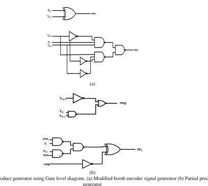
Fig 1 Partial product generator using Gate level diagram. (a) Modified booth encoder signal generator (b) Partial product generator
For n*n multiplier, there will be [n/2][6] partial products generated, and the maximum height of which we get for the partial product array is [n/2] + 1.
The first row in our multiplication split into two sub rows temporary, the first one contain partial product bits (from right to left) from pp00 to pp80 while second one with two bits set at “one” in positions 9 and 8. Then, neg3 of fourth partial product row is moved to second sub row.
Table 1 RADIX 4MODIFIED BOOTH ENCODING
Y2i+1 Y2i Y2i-1 Generated Partial Product
0 0 0 0x
0 0 1 1x
0 1 0 1x
0 1 1 2x
1 0 0 -2x
1 0 1 -1x
1 1 0 -1x
1 1 1 -0x
Aim of doing this is second sub row containing also the bit neg3, can now be easily added to the first sub row, with a constant short carry propagation of three positions i.e., independent of the length of the operands, for square multipliers. In fact, with reference to the notation of Fig. we have that qq90 qq90 qq80 qq70 qq60 ¼ 0 0 pp80 pp70 pp60 + 0 1 1 0 neg3.
IJEDR1403027
International Journal of Engineering Development and Research (www.ijedr.org)3063
x7 x6 x5 x4 x3 x2 x1 x0
y7 y6 y5 y4 y3 y2 y1 y0
PP80 PP70 PP60 PP50 PP40 PP30 PP20 PP10 PP00
1 1 neg3
1 PP81 PP71 PP61 PP51 PP41 PP31 PP21 PP11 PP011 neg0
1 PP82 PP72 PP62 PP52 PP42 PP32 PP22 PP12 PP02 neg1
1 PP83 PP73 PP63 PP53 PP43 PP33 PP23 PP13 PP03 neg2
(a)
x7 x6 x5 x4 x3 x2 x1 x0
y7 y6 y5 y4 y3 y2 y1 y0
qq90 qq80 qq70 qq60 PP50 PP40 PP30 PP20 PP10 PP00
1 1 neg3
1 PP81 PP71 PP61 PP51 PP41 PP31 PP21 PP11 PP011 neg0
1 PP82 PP72 PP62 PP52 PP42 PP32 PP22 PP12 PP02 neg1
1 PP83 PP73 PP63 PP53 PP43 PP33 PP23 PP13 PP03 neg2
(b)
Fig 2 Partial product after adding the neg value to the first row (a) Basic (b) Resultant array.
For 1st partial product row we use this circuit which contain all previous mentioned signal one, two, and neg as shown in the fig 3.
One0
Two0
Neg0
y0
y1
One0
xj
Xj-1
two0
neg0
pp0j
(a) (b) Fig 3: First row partial product generator
B. Bypass zero feed a direct (BZFAD)
This work totally deals with the low power architecture and the architecture which uses this technique of BZFAD the main reason behind that is other architecture like shift and adds multiplier ,carry select adder and tree multiplier in all this multiplier shift and add consider as the best just because of simple deign and area.
So to achieve low power we need to deal with few parameters i.e. according to formula so here different parameter that are used to reduce power are capacitance , voltage and frequency and in this work we are reducing the switching activity that is another factor on which power directly proportional.
Two multiplier implemented in this paper first is conventional and second one is BZFAD. First design i.e. conventional multiplier, in that multiplier every time there is a requirement of shifting B bit. For any particular multiplier we have six major sources of switching activity they are (1) shifting value of B register, (2) counter activity, (3) adder activity, (4) „0‟ and A switching between in the multiplexer, (5) multiplexer select activity, (6) partial product shifting. So this paper can conclude that power can be minimized by reducing any of the above mentioned parameter. Still there is a need for more optimized then one can reduce by switching activity of higher capacitance nodes.
IJEDR1403027
International Journal of Engineering Development and Research (www.ijedr.org)3064
Bypass
Feeder
Ring counter
Plow (latch)
Ready
Cout
mux1 B(n+1)
K K
K+1
K
B
K
M1
M2 PP(k to 1)
~clock ~clock
B(n)
PP(0)
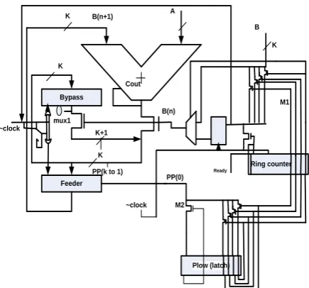
Fig 4 Architecture of Bypass zero feed a direct
In first architecture register B should be shifted to the right in every clock cycle. This depends on the value of right bit of B (0). B (0) (multiplier) bit is used to select particular value of A (multiplicand) and „0‟ value. If B (0) is equal to one then A should be added to partial products while if B (0) is equal to zero, then „0‟ should be added to partial product. Afterwards rights shifting of B on the basis of partial product in each cycle give rise to switching activities. So on the basis of the value of the „B(0)‟ select the required bit of B(0) without shifting partial products in each clock cycle to avoid this we use low power ring counter. The 2nd architecture (BZFAD) [8] architecture uses a multiplexer to choose the particular bit of B (0).
2) Feeder and bypass register operation - In the conventional multiplier (1st architecture) on the basis of the right most bit of „B‟, multiplier do the further process like if bit is „0‟ then it will add the zeros to the partial product otherwise value og A (multiplicand) by shifting one bit every time and finally we get the output that why it takes more power because no. Of transition increases so we can decrease this by bypass this zero partial product with the help of bypass and feeder register [9].Both these register are use to bypass the adder in cycles in which the B (0) is equal to zero. In each clock cycle the next bit is checked and these operations are performed:
Feeder is clocked if B (0) in next cycle is “1” Bypass is clocked if B (0) in next cycle is “0”
3) Ring Counter - In the 2nd architecture (BZFAD) we use ring counter of wider width just because of the reason that if we use any other binary counter then number of transition will increase and dynamic power increases so due to this we use chain of d flip flop which act as a ring counter as all of the flops having common clock and this can be further reduce by applying clock gating circuit to the input and check the input or the if the output is one then only enable the clock circuit so this further can reduce the switching activity or power consumption and the output store in the latch but if we apply this clock gating circuit to all the flip flop then area will increase and this will become another concerning factor so that why we are using for ingle flip flop [10].So on the basis of that this work one can conclude the low power ring counter have their own advantage in achieving low switching activity and power.
III. RESULTS
TABLE 2 Results showing area and power required
AREA REPORT (um2) POWER REPORT (nW) Modified booth multiplier 1398 449368.787
BZFAD 10864 166368.040
IJEDR1403027
International Journal of Engineering Development and Research (www.ijedr.org)3065
Fig 5 Chip plan and layout information of BZFADIV. CONCLUSIONS
This paper and its study show that low power multiplier is implemented which basically deals with the bypassing of zero in the multiplier bit and use of ring counter in spite of conventional one which deal with both the thing i.e. zero bit and binary counter which both leads to more power consumption and area. By comparing both the design we can say that BZFAD consume low power. Beside all this further work can be done in terms of clock gating which can further reduce the power consumption .so on the basis of all the results and lab work we can conclude BZFAD is one of the best choices in terms of low area and power, here final chip plan of this is shown in fig 5.
REFERENCES
[1] O.L. MacSorley, “High Speed Arithmetic in Binary Computers,” Proc. IRE,vol. 49, pp. 67-91, Jan. 1961. [2] L. Dadda, “Some Schemes for Parallel Multipliers,”Alta Frequenza, vol. 34, pp. 349-356, May 1965
[3] J C.S. Wallace, “A Suggestion for a Fast Multiplier,”IEEE Trans. Electronic Computers,vol. EC-13, no. 1, pp. 14-17, Feb. 1964.
[4] D.E. Shaw, “Anton: A Specialize Machine for Millisecond-Scale Molecular Dynamics Simulations of Proteins,”Proc. 19th IEEE Symp. Computer Arithmetic,pg. 3, 2009.
[5] J.-Y. Kang and J.-L. Gaudiot, “Simple High-Speed Multiplier Design,”IEEE Trans. Computers,vol. 55, no. 10, pp. 1253-1258, Oct. 2006.
[6] J.-Y. Kang and J.-L. Gaudiot, “A Fast and Well-Structured Multiplier,”Proc. Euromicro Symp. Digital System Design,pp. 508-515, Sept. 2004.
[7] F. Lamberti, N. Andrikos, E. Antelo, and P. Montuschi, “Speeding-Up Booth Encoded Multipliers by Reducing the Size of Partial Product Array,” internal report, http://arith.polito.it/ ir_mbe.pdf, pp. 1-14, 2009.
[8] Reducing the Computation Time in (Short Bit- Width) Two‟s Complement Multipliers Fabrizio Lamberti,Member, IEEE, Nikos Andrikos, Student Member, IEEE, Elisardo Antelo,Member, IEEE, and Paolo Montuschi, Senior Member, IEEE, IEEE transactions on computers, vol. 60, no. 2, february
[9] Low power shift and add multiplier design, c. N.MarimuthuDr. P. Thangaraj, Aswathy Ramesan, International Journal of Computer Science and Information Technology, Volume 2, Number 3, June 2010.