ISSN (Print) : 2320 – 3765 ISSN (Online): 2278 – 8875
I
nternational
J
ournal of
A
dvanced
R
esearch in
E
lectrical,
E
lectronics and
I
nstrumentation
E
ngineering
(An ISO 3297: 2007 Certified Organization)
Vol. 5, Issue 7, July 2016
Design and Implementation of Hamming Code
Technique Used for providing security to
128-bit Digital Data with Error Detection and
Correction written in VHDL Code
Sonam Barik1 , Paresh Kumar Pasayat2
M.Tech. Student [ETC], Dept. of ETC Engg., I.G.I.T. Government Engineering College, Odisha, India
Assistant Professor, Dept. of ETC Engg., I.G.I.T. Government Engineering College, Odisha, India
ABSTRACT:The proposed work deals with the technique to encode 128-bit digital data at the transmitter end using Hamming code technique & it also provides the logic used to detect and correct the error in the received data at the receiver end (if any).The encoding has been done by dividing the 128-bit data into 32 nos. of word each consisting of 4-bit. After that, the 7-bit Hamming (7, 4) code technique has been used in all the 32 words to generate 7-bit encoded data and the corresponding 7-bit encoded datas generated from each word are appended to form 224-bit data. This data is transmitted from source station to destination and the logic has been implemented to detect and correct the error. This design is having various advantages likes high data width (i.e. 128-bit), less combinational path delay and less power consumption because of simplicity in the design. This work can best be implemented in the field of telecommunication, banking sector, military sector.
KEYWORDS: ALU (Arithmetic Logic Unit), RTL (Register Transfer Level), VHDL (Very High speed Integrated Circuit Hardware Description Language).
I. INTRODUCTION
Data security is a technique used to provide security to the data so that the data can be received with zero-error at the receiver end & the data security unit should ensure that the received data is the exact replica of the data transmitted at the transmitter end. The proposed design aims to design the encoding unit for the encoding of 128-bit digital data, error detection unit to find out the error(s) in the received data and error correction unit to correct the error in the received data unit using “Hamming Code Technique”.
II.SYSTEM MODEL
ISSN (Print) : 2320 – 3765 ISSN (Online): 2278 – 8875
I
nternational
J
ournal of
A
dvanced
R
esearch in
E
lectrical,
E
lectronics and
I
nstrumentation
E
ngineering
(An ISO 3297: 2007 Certified Organization)
Vol. 5, Issue 7, July 2016
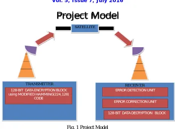
Project Model
TRANSMITTER
128-BIT DATA ENCRYPTION BLOCK using MODIFIED HAMMING(224,128)
CODE
RECEIVER
128-BIT DATA DECRYPTION BLOCK
SATELLITE
ERROR DETECTION UNIT
ERROR CORRECTION UNIT
Fig. 1 Project Model
III. ALGORITHMS USED IN THE PROPOSED DESIGN
A. Algorithm For Encoding Unit Step 1
First, 128-bit data is divided into 32 nos. of words each consisting of 4-bit data.
Step2
The 7-bit Hamming (7,4) code encoding technique is applied to each word. For each word, the encoding unit generates 7-bit encoded data. The logic for implementing the Hamming code technique is given as follows:
Suppose, the 4-bit data (B) to be encoded is B3B2B1B0 and the 7-bit Hamming code (H) generated is H6H5H4H3H2H1H0.
Here, the value for each bit of H is given as follows: H6 = B3 xor B2 xor B0
H5 = B3 xor B1 xor B0 H4 = B2 xor B1 xor B0 H3 = B3
H2 = B2 H1 = B1 H0 = B0
Step 3
After that the Hamming codes corresponding to each word are appended to form the desired 224-bit encoded data.
B. Algorithm For Error Detection And Correction Unit Step 1
To decode a Hamming code, checking needs to be done. The decoding has been done in word-by-word basic. Let us take A2A1A0 be a parity word consisting of three bits which is used to detect the error in the received data. The values of A are given as follows:
ISSN (Print) : 2320 – 3765 ISSN (Online): 2278 – 8875
I
nternational
J
ournal of
A
dvanced
R
esearch in
E
lectrical,
E
lectronics and
I
nstrumentation
E
ngineering
(An ISO 3297: 2007 Certified Organization)
Vol. 5, Issue 7, July 2016
A2 = H6 xor H5 xor H4 xor H3
Step 2
If the value of A2A1A0 is equal to “000”, then there is no error in the received data and the data can be decoded to get the exact replica of the transmitted data.
Step 3
If the value of A2A1A0 is not equal to “000”, then there is error in the received data and the checking is done in which bit, the error is present. For example, A2A1A0 = “001”, then the first bit of H from MSB is having error.
Step 4
In order to correct the error, the bit of H in which the error is present has to be complemented (i.e. ‘0’ is replaced by ‘1’ and ‘1’ is replaced by ‘0’). After correcting the error, the corrected encoded data can be decoded by using decryption algorithm.
C. Algorithm for Receiver Unit Step 1
In order to decode the 224-bit corrected encoded data, the data is divided into 32 nos. of blocks each generating 7-bit encoded data.
Step 2
Then, the following logic has been used to obtain the original 128-bit data transmitted at the transmitter end after appending all 4-bit data generated from 32 nos. blocks used for decoding unit in the receiver circuit. Let us take, the 7-bit corrected encoded data is C & the 4-7-bit data generated from the decoding unit is R.
Where C=C(6) & C(5) & C(4) & C(3) & C(2) & C(1) & C(0) R=R(3) & R(2) & R(1) & R(0)
R(0) = C (0) R(1) = C (1)
R(2) = C (2)
R(3) = C (4)
Step 3
The step has been repeated for all the 32 nos. of blocks each consisting of 7-bit corrected encoded data input. All the 4-bit output datas (R) are appended to produce 128-bit decoded data which is the exact replica of the 128-bit data transmitted at the transmitter end.
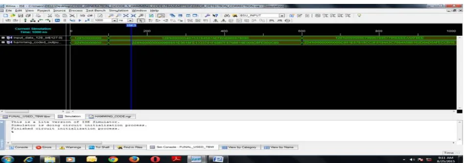
IV. RESULT AND DISCUSSION
The code of the proposed design has been written in VHDL language and tested and simulated using Xilinx software. The simulation result of the encryption unit using Hamming code technique is given as follows:
ISSN (Print) : 2320 – 3765 ISSN (Online): 2278 – 8875
I
nternational
J
ournal of
A
dvanced
R
esearch in
E
lectrical,
E
lectronics and
I
nstrumentation
E
ngineering
(An ISO 3297: 2007 Certified Organization)
Vol. 5, Issue 7, July 2016
In the above simulation result, one 128-bit digital is given as input to the hamming code unit and the corresponding 128-bit encrypted data has been obtained which is transmitted to the space.
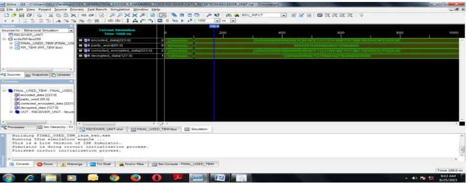
Similarly, the simulation result of the 128-bit decryption unit is obtained in which 128-bit encrypted data is given as the input to the decryption unit and the original 128-bit data has been recovered from the decrypted data. The simulation result of the decryption unit 1st set of encrypted data is given as follows:
Fig. 3 Simulation result of the decryption block with 224-bit as the encrypted data corresponding to the 1st input data
The simulation result of the decryption unit 2nd set of encrypted data is given as follows:
Fig. 4 Simulation result of the decryption block with 224-bit as the encrypted data corresponding to the 2nd input data
ISSN (Print) : 2320 – 3765 ISSN (Online): 2278 – 8875
I
nternational
J
ournal of
A
dvanced
R
esearch in
E
lectrical,
E
lectronics and
I
nstrumentation
E
ngineering
(An ISO 3297: 2007 Certified Organization)
Vol. 5, Issue 7, July 2016
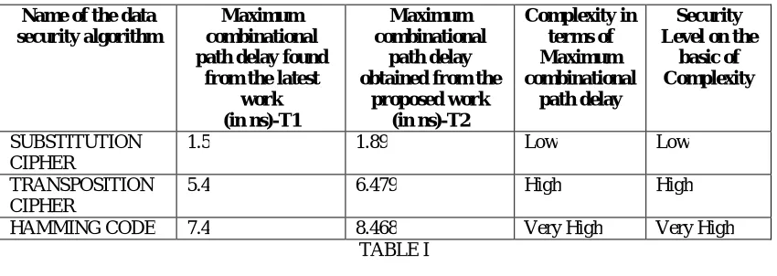
Name of the data security algorithm
Maximum combinational path delay found
from the latest work (in ns)-T1
Maximum combinational
path delay obtained from the
proposed work (in ns)-T2 Complexity in terms of Maximum combinational path delay Security Level on the
basic of Complexity
SUBSTITUTION CIPHER
1.5 1.89 Low Low
TRANSPOSITION CIPHER
5.4 6.479 High High
HAMMING CODE 7.4 8.468 Very High Very High TABLE I
V. ADVANTAGES
The proposed work is having various advantages such as providing data and network securities, low power consumption, better combinational path delay due to the better placement of modules, simultaneous transmission of higher bit data (i.e. 128-bit) etc.
VI. APPLICATIONS
The proposed design can be used in the field of banking sector, military sector, telecommunication industry and any other sectors which are used to communicate with the people within the organization using data security techniques (intranet & internet).
VII. CONCLUSION
At the end of the proposed work, the data security unit has been successfully designed with error detection and correction of 128-bit digital data using VHDL code and the desired results have been obtained. The proposed design is having less combinational path delay resulting faster operation.
REFERENCES
[1] Rekha Halkatti,Veeresh Pujari,“FPGA based 128-bit customised vliw processor for executing dual scalar/vector instructions”, NCRIET, Vol. 03, Special Issue: 03, 2014.
[2] Marri Mounika, Aleti Shankar, “Design & Implementation of 32-Bit Risc (MIPS) Processor”, International Journal of Engineering Trends and Technology (IJETT), Vol. 4, Issue: 10, 2013.
[3] Balpande, R.S. and Keote, R.S., "Design of FPGA based Instruction Fetch & Decode Module of 32-bit RISC (MIPS) Processor", International Conference on Communication Systems and Network Technologies, pp. 409-413, 2011.
[4] Manoranjan Pradhan, “Simulation and Verification of Self Test 16-Bit Processor”, International Journal of Computer Applications, Vol. 20, pp.42-45, 2011.
[5] Nupur Gupta, Progoti Gupta, Himansi Bajpai, Richa Singh,Shilpa Saxena,”Analysis of 16 bit Microprocessor Architecture on FPGA using VHDL” International journal Of Advanced Research in Electrical, Electronics and Instrumentation Engineering, Vol. 3, Issue: 4, 2014.
[6] W.Stallings,“Cryptography and Network Security”, 2nd Edition, Prentice Hall.
[7] Christof Paar, Jan Pelzl, "The Data Encryption Standard (DES) and Alternatives", "Understanding Cryptography", Springer. [8] Bruce Schneir: Applied Cryptography, 2nd edition, John Wiley & Sons.
[9] A.Litwin, “Cryptography and Network Security” LOS Alamitos,CA:IEEE computer society press. [10] Douglas L. Perry. “VHDL Programming by Examples”, TMH.